
Abstract
This paper describes the annihilation behavior of void defects in Czochralski silicon wafers during ultrahigh-temperature rapid thermal oxidation (RTO) at temperatures over 1300°C. Our results clearly demonstrate that ultrahigh-temperature RTO can provide not only the control of oxygen precipitation nuclei, but also annihilation of void defects. It is estimated from point defect calculations that the Ci/Cieq ratio still remains supersaturated because of the oxidation of the Si surface even though the type of the dominant point defect changes from interstitial Si to vacancies during ultrahigh-temperature RTO.

This is an open access article distributed under the terms of the Creative Commons Attribution 4.0 License (CC BY, http://creativecommons.org/licenses/by/4.0/), which permits unrestricted reuse of the work in any medium, provided the original work is properly cited.
Oxygen precipitates (OPs) in a Czochralski silicon (Cz-Si) wafer can degrade the performance of semiconductor devices if they are in the active region of the Si wafer, i.e., the surface layer. On the other hand, they can improve device fabrication yield through their ability to enhance impurity gettering and through mechanical strengthening, both of which are important characteristics for semiconductor device fabrication.1,2 Thus, the OPs must be controlled in an appropriate manner depending on the structure of the intended semiconductor devices and the production process employed. More precise and uniform control of OPs in Si wafers will be a significant factor for future advanced semiconductor devices. To understand this very important issue, we previously investigated the re-formation effect of OP nuclei using ultrahigh-temperature rapid thermal oxidation (RTO), at over 1300°C, and achieved wide and precise controllability of new OP nuclei.3 This technique also demonstrated a remarkable ability to eliminate heterogeneity effects such as OP nuclei or related defects in the grown crystal. Ultrahigh-temperature annealing using rapid thermal processing (RTP) has significant advantages in terms of excellent temperature uniformity in the radial direction of the Si wafer as compared to the Cz-Si crystal growth process.
As mentioned above, ultrahigh-temperature RTO showed a remarkable ability to control the effects of the OP nuclei. The behavior of OP nuclei in Cz-Si crystals is strongly related to point defects such as vacancies and Si interstitials.4 Vacancies promote the formation of OP nuclei because these nuclei are formed as a complex between oxygen atoms and vacancies. It is generally known that annealing in an oxygen atmosphere is not a practical way to increase vacancy concentration because Si interstitials are dominant in the Si wafer due to the injection of Si interstitials from the oxidized surface. However, as we previously reported,3 the behavior of OP nuclei can be controlled by changing the dominant point defects from Si interstitials to vacancies depending on the difference of each thermal equilibrium concentration at ultrahigh temperatures, even though the oxidation atmosphere is used for RTP. Furthermore, in the case of ultrahigh-temperature RTO, it is expected that Si interstitials also exist at high concentration due to the Si surface oxidation even though the dominant point defects are vacancies. Interstitial Si point defects are expected to annihilate vacancy-related defects such as void defects when enough interstitial Si atoms exist.5 The void defects also influence the semiconductor device performance; therefore, in addition to OP control, annihilating void defects is a very important goal. It is well known that RTP in a nitrogen or argon atmosphere does not effectively annihilate void defects under the surface of the Si wafer.6–8 Ultrahigh-temperature RTO would gain a further advantage over RTP in a nitrogen or argon atmosphere if annihilation of void defects is confirmed. In this study, the annihilation behaviors of void defects in the case of the ultrahigh-temperature RTO were evaluated in detail.
Nitrogen-doped Si (100) wafers, 300 mm in diameter, were cut from three Cz-Si single crystals. Nitrogen-doped Si wafers were used to reduce the void defect size so that the elimination effect of RTO can be easily observed. The oxygen concentration (according to the old American Society for Testing and Materials (ASTM) standards), nitrogen concentration, and resistivity of the tested wafers were 1.13–1.30 × 1018 cm−3, 1.9–3.8 × 1014 cm−3, and 27.2 Ω·cm (boron-doped), respectively. A commercially available RTP unit was used from 1200–1375°C for 15 s to anneal the wafers in a pure O2 atmosphere in order to introduce point defects in the Si wafer. The cooling rates to 600°C were a maximum of 120 K/s. These conditions were the same as those used in our previous study, which reported the formation of OP nuclei due to RTO.5 After each RTO, chemical-mechanical polishing was used to remove material from the wafer surface to a depth of 8 μm because the void defects in high oxygen concentration areas due to RTO, which diffuses the oxygen, cannot be annihilated.6 After chemical-mechanical polishing, the void defects of the surface layer from the surface to a depth of 5 μm were measured by a laser scattering tomography defect (LSTD) scanner (Raytex MO-601). The measurement area of the LSTD scanner was one-quarter of the wafer. The detection limit for LSTD of the LSTD scanner was 55 nm. The edge exclusion of the LSTD measurement was 10 mm. Next, the wafer that had been treated by RTO at 1375°C was annealed at 780°C for 3 h followed by 1000°C for 16 h (the process called two-step annealing) in a pure O2 atmosphere using a commercially available vertical batch furnace to grow the OPs from the nuclei introduced in RTO. The density of OPs at wafer depths of 7–380 μm was evaluated by IR tomography (Raytex MO-441); the detection limits for size and density were 25 nm and 1 × 106 cm–3, respectively.
Typical images of LSTD are shown in Fig. 1. A large number of LSTDs were observed near the center of the wafer without RTO; the LSTD density of this wafer was 191.0 cm−2. Almost all of these LSTDs at the center of the wafer surface were confirmed to be void defects by scanning electron microscopy observation. It is well known that void defects are formed by the aggregation of vacancies, and it is relatively easy to form void defects at the center in the vacancy-rich Cz-Si crystal because the vacancy concentration is higher there than in other areas.9 Therefore, we will describe those LSTDs at the wafer center as void defects. It is clear that the number of void defects decreased as the RTO temperature increased. In the case of the wafer subjected to RTO below 1300°C, the density of void defects was decreased to about 6.7–12.3 cm−2. The annihilation of void defects was enhanced by increasing the RTO temperature to over 1300°C. Although the duration of the RTO used in this study was relatively short, the annihilation effects at over 1300°C were remarkable, and the densities of void defects were reduced to less than 1.0 cm−2.
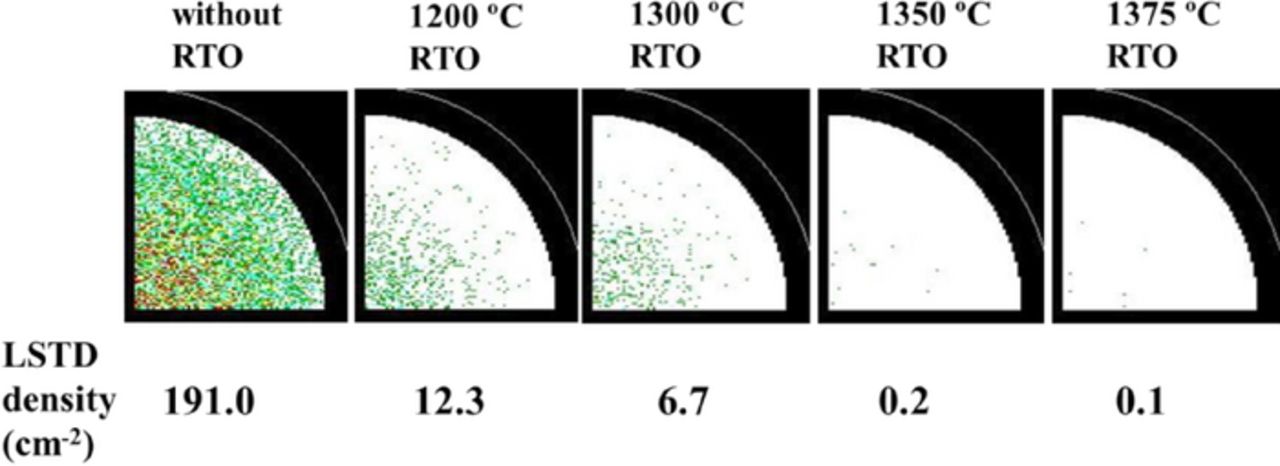
Figure 1. Relationship between RTO temperature and LSTD density.
We now discuss the OPs in the samples without RTO and with RTO at 1375°C and two-step annealing. OPs were observed in the case of the wafer without RTO, but the density of the OPs varied with position on the wafer. The density of OPs decreased abruptly at a radius of approximately 110–145 mm from the wafer center due to the oxide-induced stacking fault ring (OSF ring) region which is formed during Cz-Si crystal growth.9 Unlike the wafer without RTO, a uniform distribution of OPs was observed as a function of radial distance in the case of the 1375°C RTO wafer. The OPs were very dense and very fine in the bulk of each wafer as shown in our previous report (Reference 3, Fig. 2). The reason is believed to be that a fresh nucleation of OPs, which is different from that of Cz-Si crystal growth, was uniformly initiated by the ultrahigh-temperature RTO.5 From these results, it was confirmed that the ultrahigh-temperature RTO at 1375°C is able to provide both the annihilation of void defects and the formation of new OP nuclei.
As mentioned above, it is generally known that both the annihilation of void defects and the formation of new OP nuclei are related strongly to the behavior of point defects such as vacancies and Si interstitials during RTP. High concentrations of interstitial Si are needed to annihilate void defects effectively. On the other hand, for the formation of new OP nuclei, a high concentration of vacancies is required. Reported examples indicate that it is very difficult to control these balances.10 However, ultrahigh-temperature RTO might have a strong advantage that can increase concentrations of both interstitial Si and vacancies because each equilibrium concentration increases as a function of the increasing RTO temperature; in addition, the oxidation of the Si surface helps to increase the interstitial Si concentration. Therefore, the values of Cv (concentration of vacancies) and Ci (concentration of interstitial Si) were estimated for a better understanding of the experimental results. The Cv − Ci depth profile corresponding just after each RTO (800°C) was estimated by numerical simulation using techniques described in the prior literature.5,11--13 The average oxidation rates for RTO experiments, which were used for the numerical simulation, were obtained with an ellipsometer (SOPRA GES-5E), and were estimated to be 1.9 or 6.9 μm/h at 1200 or 1375°C, respectively. The calculated Cv − Ci depth profiles are shown in Fig. 2. For the 1375°C RTO, the calculated Cv − Ci in bulk is over 9 × 1012 cm−3, which was assumed to be the critical value for the formation of OP in our previous study5 and also by Akatsuka et al.10 It is believed that the OP nuclei were effectively formed by keeping Cv high. Thus, from Fig. 2, the dominant point defect after 1375°C RTO is assumed to be the vacancy. On the other hand, the annihilation of void defects was also confirmed at those RTO conditions in this experiment. The Ci/Cieq ratio (where Cieq = the equilibrium concentration of interstitial Si) at the maximum duration temperature is considered the key parameter for the annihilation of void defects; it was calculated by the method proposed by Taniguchi et al.13 and is shown in Fig. 3. The Ci/Cieq ratio decreases gradually as the temperature increases. However, it can be seen that Ci/Cieq still remains supersaturated (about 2.3) even in the case of 1375°C RTO, which means there are enough interstitial Si atoms to annihilate the void defects. The annihilation effect of void defects occurred effectively at higher temperature RTO conditions because of the quick dissolution of the oxide film on the inner wall of the void defect and the generation of numerous Si interstitials that bury the void defect without an oxide film on the inner wall. The Ci values can be estimated from the Cieq at each temperature in Reference 11 and calculated Ci/Cieq in Fig. 3. The Ci values at 1200°C, 1300°C, 1350°C, and 1375°C RTO were obtained to be about 4.2 × 1013 cm−3, 2.1 × 1014 cm−3, 4.0 × 1014 cm−3, and 6.0 × 1014 cm−3, respectively. From Fig. 2 and Fig. 3, it can be seen that the dominant point defect induced by ultrahigh-temperature RTO is the vacancy, but Ci/Cieq still remains super-saturated. Thus, we concluded that this is the reason why the formation of new OP nuclei and the annihilation of void defects occurred simultaneously in the RTO process.
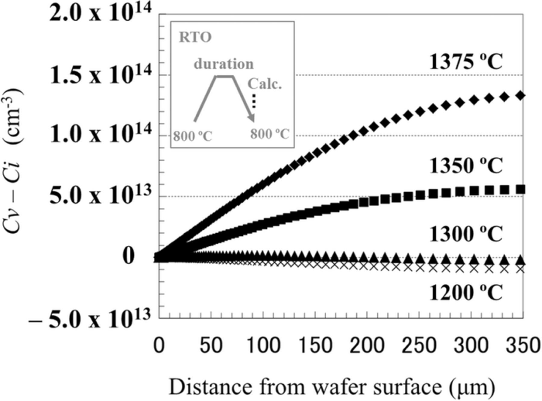
Figure 2. Depth profile of the calculated Cv − Ci concentration for RTO with a cooling rate of 120 K/s.
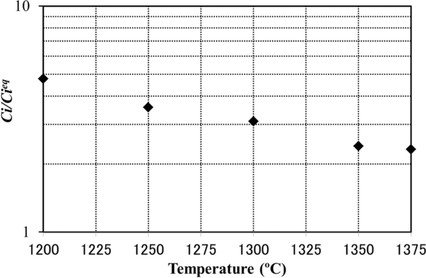
Figure 3. Supersaturation of interstitial Si atoms at SiO2/Si interface as a function of oxidation temperature.
We have demonstrated the annihilation effect of the void defects by ultrahigh-temperature RTO in 300 mm diameter Cz-Si wafers. Our results clearly indicated that the ultrahigh-temperature RTO at 1375°C provided not only the control of OP nuclei, but also the annihilation of vacancy-related defects such as void defects. This technique can be applied to improve both the fundamental heterogeneity of crystals due to intrinsic point defects and the related growth of the defects.