Abstract
In this study, the development of post-chemical mechanical polishing (CMP) protocols for cleaning abrasive nanoparticles from In0.53Ga0.47As surfaces was systematically analyzed. Abrasive silica nanoparticles (130 and 289 nm) were intentionally deposited onto InGaAs surfaces. Various concentration ratios of chemical etchants such as HCl and H2O2 were used to control material loss and surface oxides of InGaAs. The optimal concentration ratio of the HCl/H2O2 cleaning solution exhibited 40% particle removal efficiency (PRE). Application of megasonic (MS) cleaning improved the PRE to 80%. To prevent particle re-contamination, ammonium dodecyl sulfate (ADS) was used as an anionic surfactant to modify surface charge in the InGaAs substrate. Addition of surfactant further improved the PRE to over 96%. Optimal cleaning of InGaAs surfaces was achieved with a combination of HCl/H2O2, surfactant, and MS.
Export citation and abstract BibTeX RIS

This is an open access article distributed under the terms of the Creative Commons Attribution 4.0 License (CC BY, http://creativecommons.org/licenses/by/4.0/), which permits unrestricted reuse of the work in any medium, provided the original work is properly cited.
The demand for the continuing miniaturization of metal-oxide semiconductor (MOS) devices in both planar and FinFET configurations coupled with the demand to increase their performance are constant challenges for developing future applications. To achieve low-power and high-performance logic devices, supply voltage scaling must be optimized.1–3 This can be achieved for n-type metal-oxide semiconductors (nMOS) via the introduction of III-V semiconductor materials such as InAs, InP, GaAs, InSb, and InGaAs, which have very high electron mobility of ∼104 cm2/(V·s), ten times greater than silicon.3–6 InGaAs is a III-V material suitable for sub-10nm logic devices due to its epitaxial matching with Si.7,8
In order to utilize InGaAs in logic devices, one or more chemical-mechanical polishing (CMP) steps are needed to obtain a planarized surface.8–10 Residual contamination from silica slurry is found on InGaAs surfaces after CMP process necessitating a post-CMP cleaning step.11 Conventional cleaning solutions based on NH4OH and DHF are limited to the surface etching and cleaning of InGaAs itself,12,13 so novel processes are required to remove contaminant particles and oxide from the substrate surface.
A few studies have explored the removal of InGaAs native oxide by using direct argon and helium plasma coupled with HCl wet chemical treatment14 and atomic hydrogen cleaning.15 Many researchers have predominantly focused on wet etching of InGaAs using acids, bases, and peroxide based mixture solutions.16–20 Wet etching of semiconductor materials generally requires oxidizing agents in suitable chemical solutions to remove the oxidized surface products. H2O2 has been widely used as an oxidizer for etching of III-V,18–21 while acidic etchants are very efficient at removing the oxide products of III-V materials.16–21 Among acidic etchants, the combination of HCl and H2O2 (HCl/H2O2) is considered one of the most suitable for InGaAs because it results in the lowest degree of anisotropy in etching.18,20 The cleaning mechanism of HCl/H2O2 involves a slight surface etching and lift-off the particles from the surface. This suggests that the formulation of post-CMP cleaning chemistry should consider both etching and particle removal. To the best of our knowledge, no reports to date have sought to optimize the removal of particles from the InGaAs surface.
The purpose of this study is to optimize the chemistry of a post-CMP cleaning solution that can clean nanoparticles from an InGaAs substrate with minimal material loss and with reduced surface oxides. We investigated wet chemical cleaning using a HCl/H2O2-based chemical etchant along with ammonium dodecyl sulfate (ADS) to meet the above goal. Here, ADS surfactant was used to prevent particle re-contamination of the InGaAs surface. Though other anionic surfactants such as sodium docdecyl sulfate (SDS) can be effective for this task, it was not used due to presence of sodium in the compound. To enhance particle removal efficiency, megasonic cleaning was applied along with the formulated chemicals for InGaAs surface cleaning.
Experimental Materials and Procedure
Materials
CMP-polished In0.53Ga0.47As wafers (12-inch, ∼75-nm thickness, IMEC, Belgium), were cut into 2-cm × 2-cm coupons for experiments. Hydrochloric acid (HCl, 35∼37%, Duksan Pure Chemicals Co., Korea) and hydrogen peroxide (H2O2, 30–32%, Dongwoo Fine Chem Co., Korea) were used for the wet etchant, and ammonium dodecyl sulfate (ADS, (CH3(CH2)10CH2OSO3NH4), ∼30%, Sigma Aldrich) was used as the surfactant for InGaAs surface etching and cleaning.
Experimental procedure
A positive photoresist (AZ-GXR 601) was employed to measure the etch rate of InGaAs. To improve the photoresist (PR) adhesion, hexamethyldisilazane (HMDS, Sigma Aldrich, USA) was first deposited onto the InGaAs surface using a spin coater (GMS-120, Genesys, Korea) followed by a soft bake at 110°C for 1 min. Then, the PR was deposited onto the substrate also via spin coating. The substrate was soft-baked on a hotplate at 100°C for 1 min before exposure. This substrate was exposed to UV light using conventional photolithography equipment (MDA-600M, MIDAS System Co., Ltd, Korea) to pattern lines onto the surface. Finally, the patterned substrate was immersed in the AZ 300K developer (AZ electronic materials, Luxembourg). The obtained line width was approximately 110 μm and depth was approximately 1 μm.
The patterned wafer was etched in various concentrations of HCl/H2O2 solution with and without adding ADS. To measure the etch depth, PR patterns were removed by acetone (J.T. Baker, USA). The InGaAs etch depth (step height) was measured by using AFM (XE-100, Park Systems, Korea) and the etch rate was calculated as,
![Equation ([1])](https://content.cld.iop.org/journals/2162-8777/8/5/P3028/revision1/d0001.gif)
The surface oxidation of InGaAs was examined before and after surface etching by X-ray photoelectron spectroscopy (XPS, Sigma Probe, Thermo, UK). The XPS experiment was performed in a UHV multipurpose surface analysis system operating at base pressures of < 10−9 mbar. The photoelectron spectra were excited by an Al Kα (1486.6 eV) anode operating at a constant power of 100 W (15 kV and 10 mA). During spectral acquisition, the constant analyzer energy (CAE) mode was employed at pass energy of 30 eV and a step of 0.1 eV. Based on the XPS results, the optimal concentration of HCl/H2O2 solution was chosen to minimize the oxide on the InGaAs surface.
For the particle cleaning experiment, silica particles (130 nm or 289 nm) were suspended in DIW and deposited on the InGaAs substrate to intentionally contaminate the surface. 100 μL of the particle suspension was spread over the substrate surface, and after a 5-min interval, the substrate was dried using nitrogen gas. These contaminated coupons were aged for 6 hours in a class 10 clean room and then particle cleaning was performed using the optimized concentration of HCl/H2O2 solution. To further enhance the cleaning efficiency, a small amount of ADS was added to the HCl/H2O2 solution to control the zeta potential and etch rate. The concentration of ADS was varied from 0.001 to 0.1 mM to keep solutions well under the critical micelle concentration of ADS of 6.7 mM. Zeta potential (ELS-Z, Otsuka Electronics Co, Japan) was measured to understand the interaction between the InGaAs surface and the silica particles with and without ADS in acidic solutions. This instrument has a platinum alloy electrode to measure zeta potential, so it is immune to the issues pertaining to the peroxide based solutions. A batch megasonic cleaning process was also employed to increase the 130-nm silica particle removal efficiency by using megasonic power of 600 W and a frequency of 1 MHz.
The InGaAs surface contamination by silica nanoparticles was measured in two different ways. Samples with 289-nm silica particles before and after nanoparticle contamination and post-cleaning were analyzed using a dark field optical microscope (LV-100D, Nikon, Japan) with a Hg lamp of 130 W power to determine the particle count. This optical microscope tool consists of an X-Y auto stage (ProScan II, PRIOR Scientific, USA) and object lenses (× 5, 10, 20, 50 and 100) with particle image analysis software (Image-pro Plus, Media Cybernetics, UK). This configuration made it possible to count the particles at the same position before and after cleaning. The wafer with 130-nm silica particle contaminants at different stages of the experiment was analyzed by FE-SEM (MIRA3, TESCAN, Czech) with particle image analysis software (Image J, 1.52e, National Institute of Health, USA). Once particle counts were obtained for the samples of either 130- or 289-nm silica particles, the PRE was calculated according to
![Equation ([2])](https://content.cld.iop.org/journals/2162-8777/8/5/P3028/revision1/d0002.gif)
where ni is the initial particle count of the as-received wafer, nb is the particle count of the intentionally contaminated wafer (using either 130- or 289-nm silica particles), and nf is the particle count after the cleaning experiment.
Results and Discussion
Various concentrations of HCl from 0.001 M to 0.05 M and H2O2 from 0 M to 0.01 M were prepared and pH value of each solution is reported in Table I. All solutions of HCl are at acidic pH and no significant changes in pH values were observed with addition of peroxide to the solutions. Etch rate experiments were performed at these concentrations and using positive PR-patterned InGaAs coupons. The etch depth of InGaAs was measured using AFM and the etch rate (Figure 1) was calculated from the etch depth and time. No significant etching occurred when InGaAs was exposed to HCl solution without H2O2. This result confirms that HCl alone cannot etch the InGaAs surface without a chemical oxidizer. Two etching regimes can be distinguished at all HCl/H2O2 conditions. The etch rate increases rapidly when the ratio of HCl to H2O2 concentration increases to 1:1. However, as this ratio increases beyond 1:1, the etch rate of InGaAs decreased. This phenomenon can be explained by the reaction between Cl and OH groups on the InGaAs surface. In the presence of H2O2, the InGaAs surface is terminated by OH groups. If the HCl concentration is higher than that of H2O2, the OH groups on the surface of InGaAs are replaced by Cl− through nucleophilic attack and it forms stabilized bond with InGaAs.18,20 D.H. van Dorp et, al. tested etching of InGaAs surface using HCl and HCl/H2O2 solution and mentioned that at high HCl concentration the surface OH groups are replaced due to nucleophilic attack by Cl− on the group III and V elements.18 The weaker electronegativity of Cl with respect to O leads to a stabilization of the back bond.20 Hence, the stabilized surface decreases the etch rate of InGaAs with high concentration of HCl than H2O2.
Table I. Measured pH values with various mixtures of HCl and H2O2 at different concentrations.
| HCl(mM)/H2O2(mM) | 0.001 | 0.005 | 0.01 | 0.05 |
|---|---|---|---|---|
| 0 | 3.44 | 2.67 | 2.34 | 1.60 |
| 0.001 | 3.45 | 2.66 | 2.34 | 1.61 |
| 0.005 | 3.46 | 2.66 | 2.33 | 1.61 |
| 0.01 | 3.44 | 2.69 | 2.35 | 1.60 |
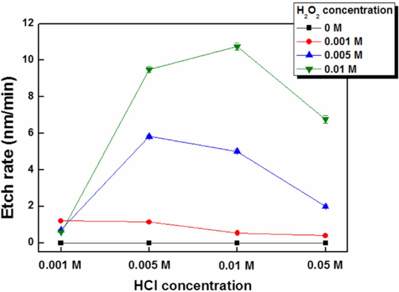
Figure 1. Etch rate of InGaAs as a function of H2O2 and HCl concentration.
To examine the effect of HCl/H2O2 etching on the surface oxide composition, the InGaAs substrates were analyzed using XPS. The binding energies of each element and the oxide composition of InGaAs before and after HCl/H2O2 treatment are given in Table II. Figure 2 shows the XPS spectra of InGaAs etched with two concentrations of HCl (0.1M, 0.001M) with 0.01M H2O2 for 1 minute. The oxide composition of as-received InGaAs was taken as a reference (Table I). Indium is active in forming the oxide in the form of In2O3.16 The oxide composition (In3d5/2 peak) was increased at low concentration HCl (0.001M) etching compared to the reference because the oxidation rate is higher than etching in the presence of high concentration of H2O2. And it can be seen that etching with a high concentration of HCl (0.1 M) reduced the oxide content. In this condition, oxidized surface of InGaAs was replaced by Cl− through nucleophilic attack and stabilize the surface. Hence, it was confirmed that the higher concentration of HCl compared to H2O2 reduces oxide formation.
Table II. Binding energy and oxide composition of InGaAs before and after HCl and H2O2 etching.
| Chemical | Binding | InGaAs (as | HCl<H2O2 | HCl>H2O2 | |
|---|---|---|---|---|---|
| Element | state | energy (eV) | received,%) | treated (%) | treated (%) |
| Indium (In3d5/2) | In2O3 | 445.0 | 21.28 | 33.54 | 18.79 |
| 452.0 | |||||
| Gallium (Ga3d5/2) | Ga2O3 | 20.5 | 23.43 | 25.25 | 21.53 |
| Arsenic (As3d5/2) | As2O5 | 44.1 | 33.80 | 34.47 | 31.01 |
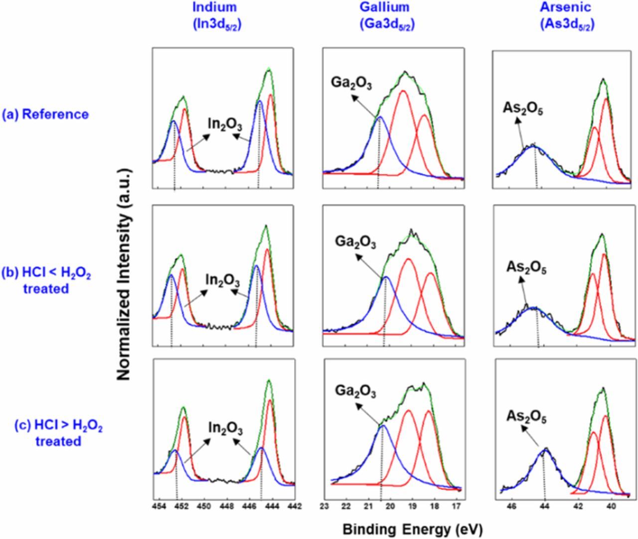
Figure 2. 3d core level XPS spectra of InGaAs surface at different conditions (a) as received (b) treated with lower concentration of HCl than H2O2, and (c) treated with higher concentration of HCl than H2O2. The solid (black) lines are XPS experimental data and the dashed lines (blue and red) are numerical fitting results.
The results of etch rate and XPS analysis, suggest that a relatively high concentration of HCl (0.05 M) and low concentration of H2O2 (0.005 M) is optimal for InGaAs cleaning to achieve the minimum material loss with controlled oxide formation. As mentioned earlier, HCl/H2O2 solutions are preferred etchants of InGaAs due to the low degree of anisotropy in their etching.18,20 Three types of etching mechanisms were proposed based on the concentration ratio of HCl and H2O2 as represented in Figure 3. The etching mechanism includes two major processes: first a self-limiting oxide is grown on the surface after which the oxide layer is removed selectively. The first etching step involves chemical hydroxylation by H2O2 on the InGaAs surface. It is generally believed that the formation of the first hydroxide layer at the surface is a slow step in the oxidation process as shown in Figure 3.18 At higher HCl than H2O2 concentration, the replacement of OH groups by Cl− ions on the polarized InGaAs surface is faster than the rupture of the back bond. The weaker electronegativity of Cl with respect to O leads to stabilization of the back bond, and hence the InGaAs etch rate is decreased. Further oxidation of the back bonds results in the formation of surface products that contain OH which enhances fast surface dissolution. At comparable HCl and H2O2 concentrations, the surface is mainly terminated with OH groups. The larger back bond destabilization results in a higher etch rate, and the dissolution rate of surface products is very fast. At lower HCl than H2O2 concentration, the dissolution rate is lower than the rate of oxide formation, because oxide dissolution can be enhanced only in the presence of sufficient HCl concentration.
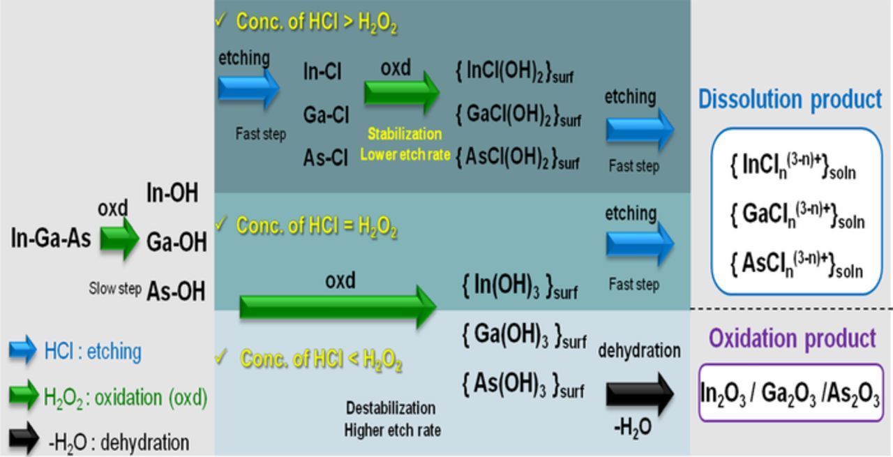
Figure 3. InGaAs etching mechanism in various concentration ratios of HCl and H2O2 cleaning chemicals.
A high concentration of HCl (0.05 M) and low concentration of H2O2 (0.001 M) was selected as the optimal cleaning solution for particle removal from InGaAs surfaces. Figure 4 shows the PRE as a function of time for 289-nm silica samples cleaned using the optimized HCl/H2O2 solution. It was observed that the PRE was increased with increased etching amount and cleaning time. PRE reached about 80% at the 3-min cleaning time, corresponding to 1.2-nm surface etching. However, particles were recontaminated on the surface and it was confirmed by comparing the change in positions of the particles before and after InGaAs particle cleaning using optical microscope measurement as shown in Figure 5. This recontamination may be due to the attractive force between the opposite zeta potentials of the silica particles and InGaAs surface.
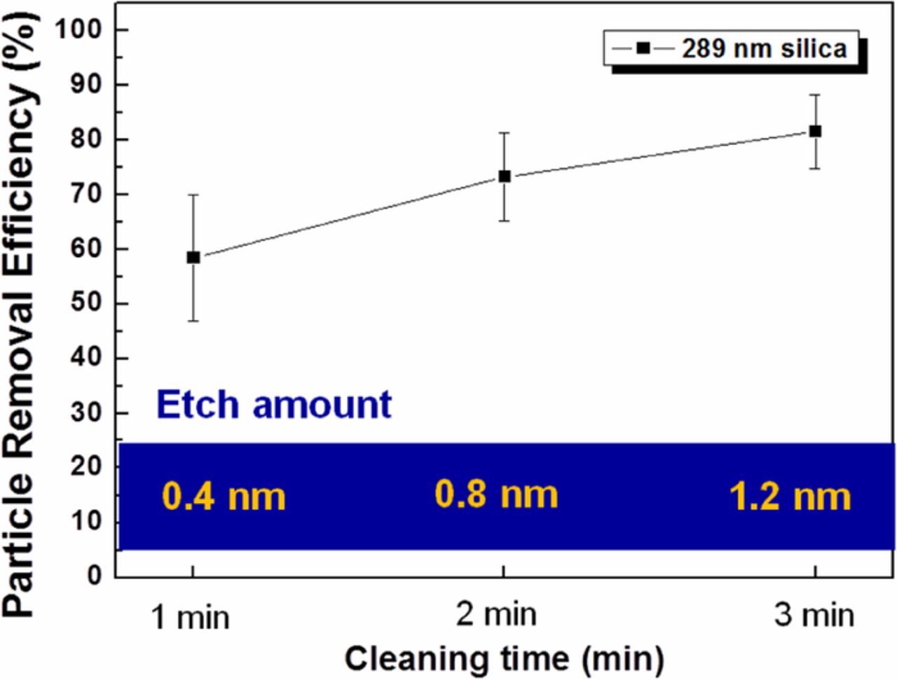
Figure 4. Silica PRE of HCl/H2O2 cleaning solution as a function of cleaning time and corresponding InGaAs etch depth.
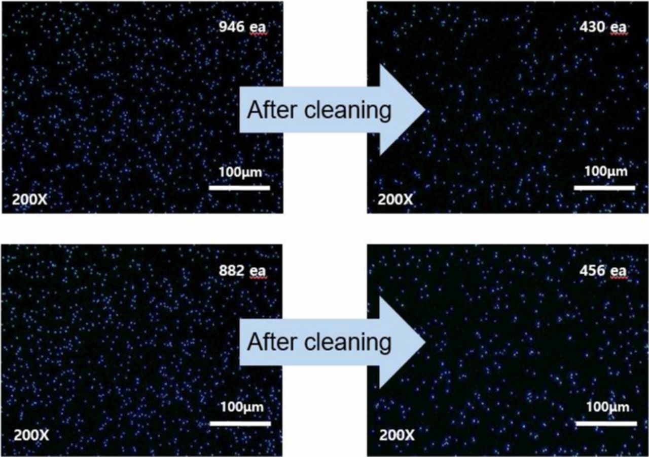
Figure 5. Dark field optical microscope images of InGaAs surface after HCl/H2O2 cleaning for 1 min.
Silica particle recontamination can be prevented by understanding the charge interaction between the particles and the substrate at various pH. This interaction can be controlled through the addition of ADS surfactant to the cleaning solution. The measurement of zeta potential of particle and substrate surface with and without ADS surfactant is shown in Figures 6 and 7. Figure 6 shows the decrease in negative zeta potential value of silica particle with increase in the pH, with no significant difference observed with or without ADS. This result indicates that the adsorbed surfactant on the particle surface does not significantly affect the zeta potential of the particles. Figure 7 shows the zeta potential values of InGaAs surface with and without ADS. The ADS addition to the cleaning solution decreased the zeta potential of InGaAs surface significantly due to ADS anions adsorbing onto the surface of InGaAs. From these results, it can be concluded that the addition of ADS to the cleaning solution results in a less attractive force acting between the particle and the substrate in acidic conditions. Hence, silica particles can be more easily removed from the InGaAs surface by using ADS in acidic solution due to the resultant electrostatic repulsion between the particles and the surface.
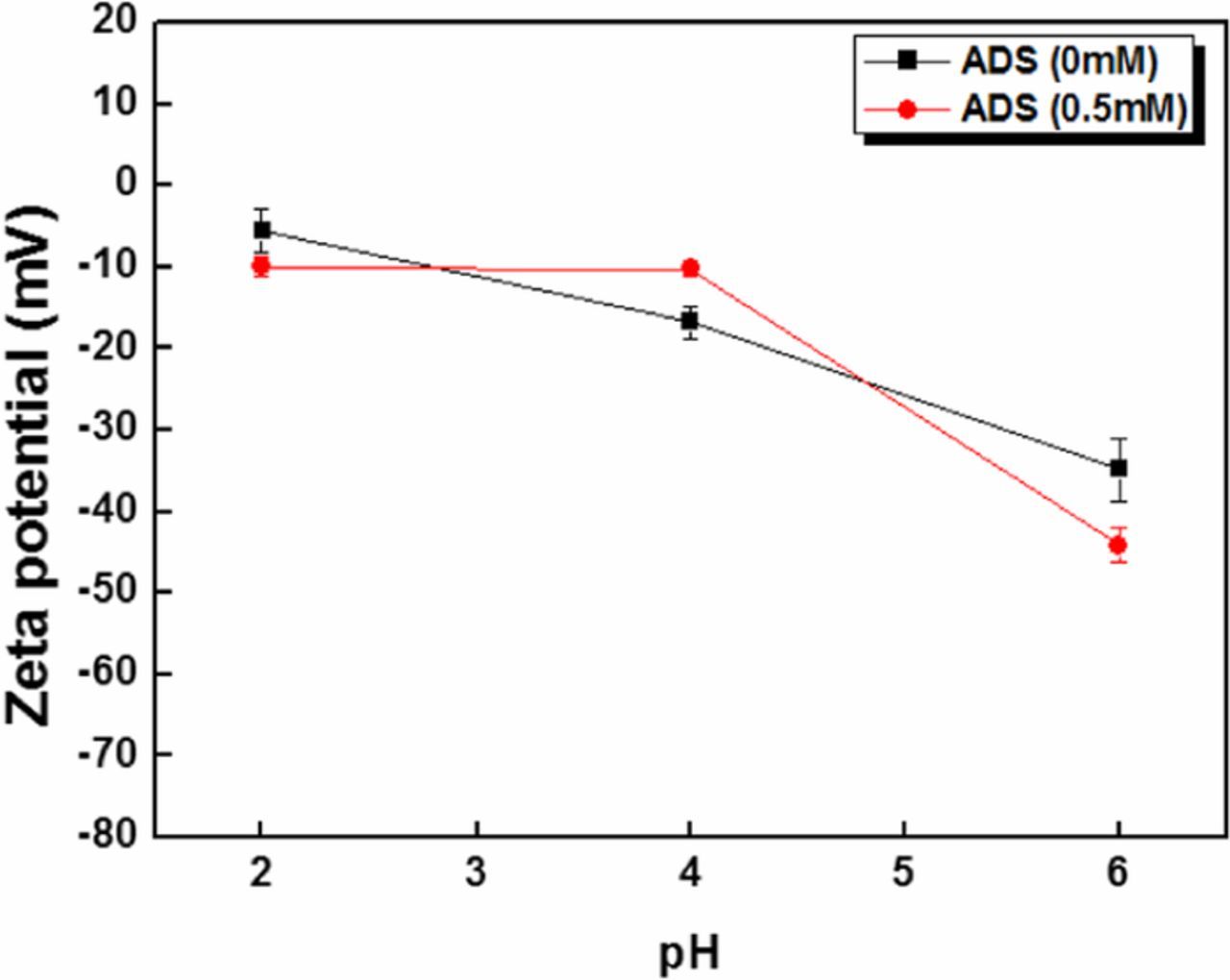
Figure 6. Zeta potential measurement of silica particles with and without ADS.
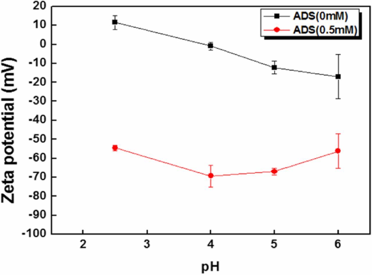
Figure 7. Zeta potential measurement of InGaAs surface with and without ADS.
Figure 8 shows the effect of surfactant concentration on the etch rate of InGaAs in HCl/H2O2 cleaning solution. There was no significant difference in the etch rate when ADS was added from 0 to 0.001 mM in the HCl/H2O2 solution. The InGaAs etch rate decreased from 0.4 to 0.1 nm/min as the ADS concentration was increased from 0.001 to 0.005 mM, and remained constant at over 0.005 mM ADS. At concentrations higher than 0.005 mM ADS, the anionic surfactant is completely adsorbed on the InGaAs surface, which decreases the InGaAs etch amount. Therefore, the required minimum amount of ADS surfactant is 0.005 mM for effective cleaning of InGaAs surface, which will modify the zeta potential value of the substrate as well as decrease the etch depth.
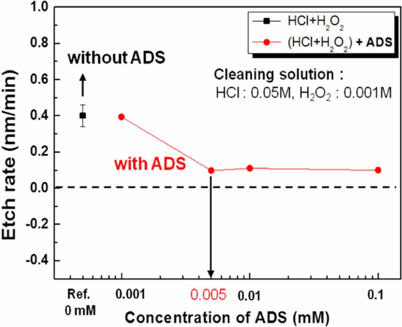
Figure 8. Etch rate of InGaAs in HCl/H2O2 cleaning solution as a function of ADS concentration.
Figure 9 shows the PRE of 130 and 289 nm silica particles cleaned via etching only and electrostatic repulsion only. The results show that 130 nm particles exhibited lower PRE than 289 nm particles when cleaned only with HCl/H2O2 solution. On the other hand, the ADS solution alone shows no noticeable removal of the contaminant silica particles. This result is consistent with the known difficulty of removing silica nanoparticles with electrostatic repulsion alone. Therefore, to remove silica nanoparticles effectively from the InGaAs surface both the etching solution and ADS are necessary. Figure 10 shows the PRE as a function of ADS concentration in HCl/H2O2 solution. The PRE increases dramatically with ADS concentration until 0.005 mM. Beyond 0.005 mM ADS, PRE continued to increase with ADS concentration, but at a lower rate. This dramatic change is due to the combined effect of surface etching and electrostatic repulsion between the surface and the particles. The zeta potential of the silica particles and InGaAs substrate was measured using the HCl/H2O2 cleaning solution with and without ADS concentration of 0.005mM. The zeta potential of InGaAs substrate was changed from +8.9 to −4.8 mV and silica particles were changed slightly −2 to −4.5 mV. Most of the 289-nm silica particles were removed (PRE 98%) in HCl/H2O2 with ADS (≥0.01 mM) solution. However, in the case of 130-nm silica particles, the PRE using the same cleaning solution is only around 85%. To increase the PRE of 130-nm silica particles, megasonic cleaning was adopted along with HCl/H2O2 with ADS cleaning solutions. Effective particle removal will therefore be achieved by using the combination of chemical interactions and physical force. Particle removal tests were performed using batch type megasonic cleaning.
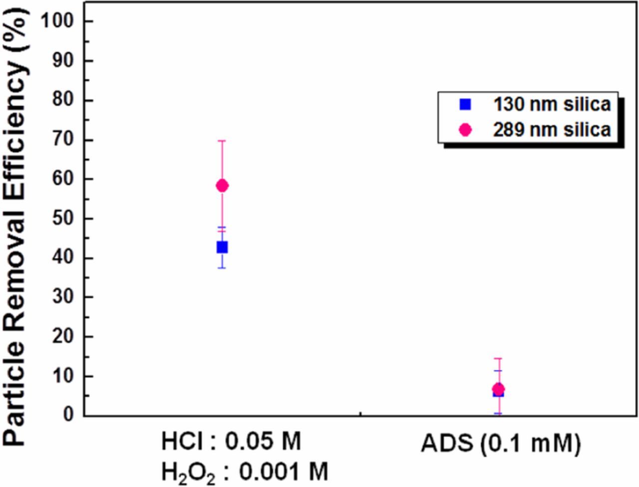
Figure 9. PRE using HCl/H2O2 only or ADS only for the removal of 130- and 289-nm silica particles.
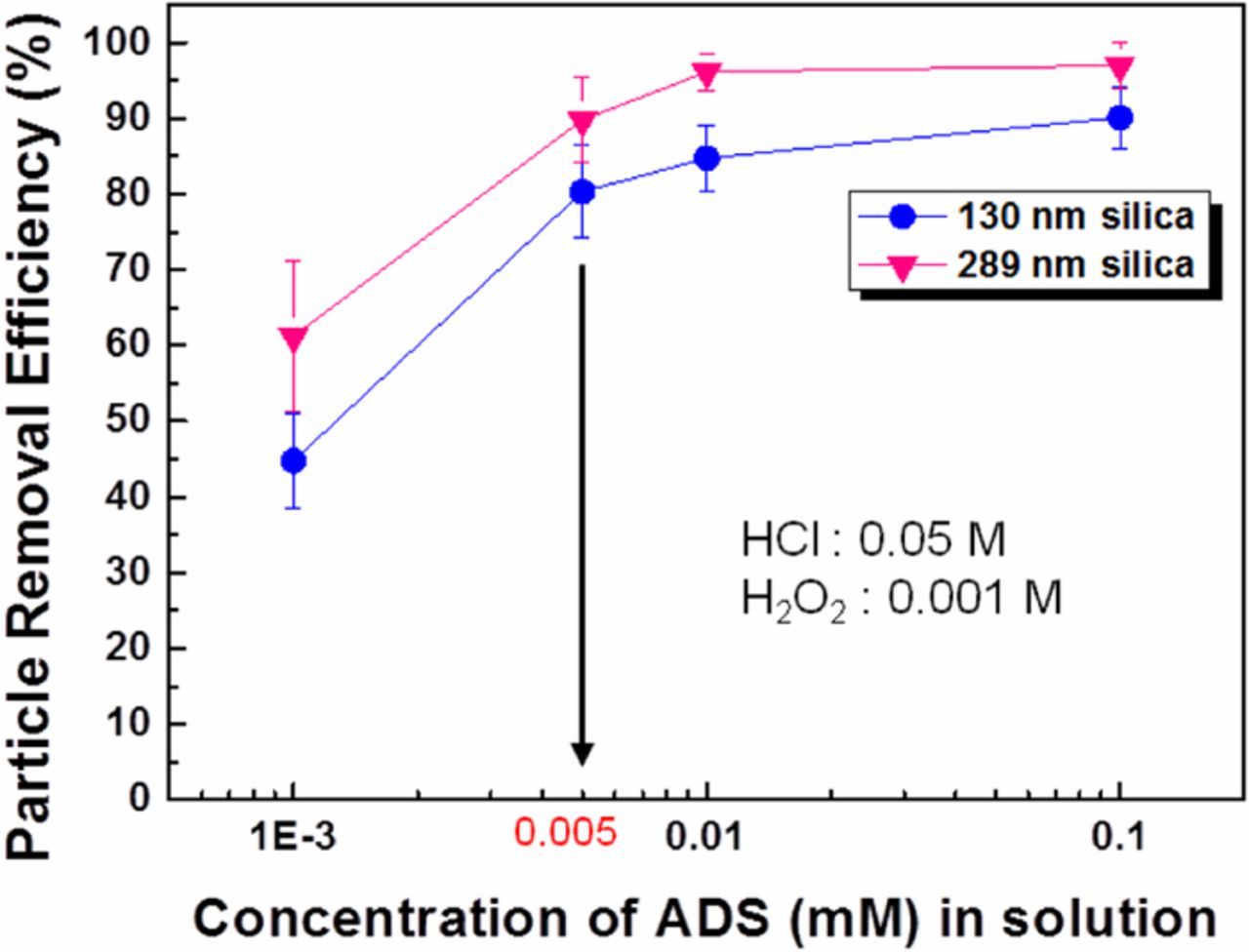
Figure 10. PRE as a function of ADS concentration in 0.05 M HCl, 0.001 M H2O2 solution for the removal of 130- and 289-nm silica particles.
Figure 11 shows the PRE results in various mixtures of HCl/H2O2 solutions with and without ADS. In the case of HCl/H2O2 with megasonic cleaning, the PRE is higher than using HCl/H2O2 solution alone. The simultaneous chemical effect of HCl/H2O2 and ADS (0.005 mM) along with megasonic cleaning removes most of the 130-nm silica particles from the InGaAs surface, with the PRE reaching around 96%. When megasonic cleaning was compared to the results without megasonic cleaning, PRE was increased by approximately 20%. This result might be due to the combined effects of megasonic, surface etching and repulsive force induced by ADS.
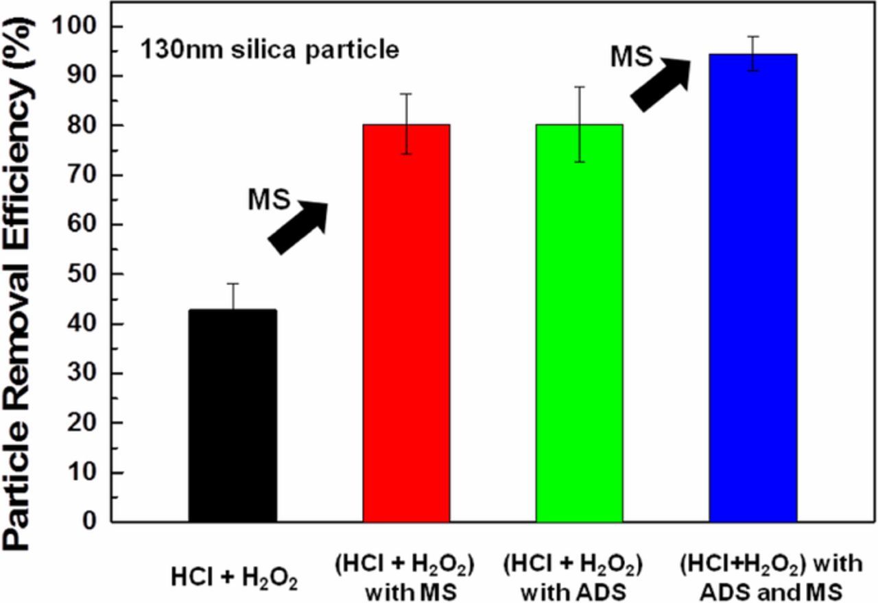
Figure 11. Effect of megasonic cleaning with various cleaning solutions on PRE of 130-nm silica particles.
Roughness is a primary factor in determining the bond between an InGaAs substrate and a film to be deposited upon it, because a rough surface is known to be a major cause of interfacial voids. Thus, an effective cleaning process for InGaAs must not significantly alter its surface roughness. The surface roughness of InGaAs before and after cleaning was analyzed using AFM and the results are shown in Figure 12. The as-received InGaAs substrate shows initial roughness of about 3.38 nm. Cleaning InGaAs under various conditions resulted in no significant change in surface roughness compared to the initial value because the etch depth was too small to significantly affect the surface roughness. Hence, the formulated cleaning solution with megasonic is a suitable cleaning method for InGaAs substrates.
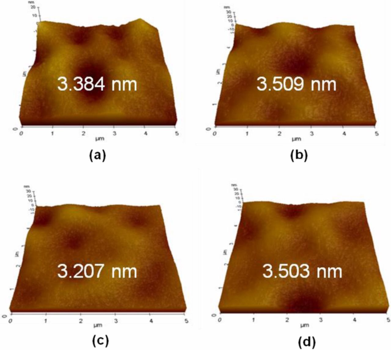
Figure 12. Surface roughness and morphologies of InGaAs surface (a) as-received and after cleaning with (b) optimized concentration of HCl/H2O2, (c) HCl/H2O2 with ADS, and (d) HCl/H2O2 with ADS and MS.
Conclusions
In this study, a post-CMP cleaning solution was formulated using HCl/H2O2 solution containing ADS surfactant for effective InGaAs surface cleaning. Varying the concentrations of HCl and H2O2 had a significant impact on the etch rate of the InGaAs substrate. Through etch rate and XPS analysis it was found that solution with a high concentration of HCl and a low concentration of H2O2 is most suitable for cleaning InGaAs with minimized material loss and minimized surface oxide. ADS was used to the solution to improve PRE. ADS decreased the zeta potential of the surface of InGaAs to more negative values which electrostatically repulsed the silica particles in the acidic conditions used for cleaning. Maximal removal of the 289- nm silica particles was achieved via cleaning with > 0.01 mM ADS in HCl/H2O2. However, chemical means alone were not effective at removing 130-nm silica particles from the InGaAs surface. To remove the 130- nm particles effectively, physical force via megasonic cleaning was applied in addition to the cleaning solution. The mixture of HCl/H2O2 and ADS with megasonic cleaning produced a PRE of about 96%. Finally, the surface roughness was evaluated using AFM before and after cleaning process. These measurements confirmed that there was no significant change in the surface roughness of the InGaAs as a result of the cleaning processes employed. Hence, it is concluded that the formulated cleaning solution with megasonic cleaning can be a suitable cleaning solution for post-CMP InGaAs substrates.
Acknowledgments
This work was supported by the Samsung Electronics' University R&D program [Physical/Chemical Research on General Defect Generation].
ORCID
Nagendra Prasad Yerriboina 0000-0003-1844-4016
Jin-Goo Park 0000-0002-8008-6478