Abstract
An Fourier Transform Spectrometer (FTS) based on an H-shaped electrothermally actuated microelectromechanical system (MEMS) scanning mirror has been developed. The MEMS scanning mirror can generate about 200 μm at 5 Hz with only 5 Vpp and maintain a very small tilting of about 0.029° without using any complex compensation or closed-loop control. This high scanning performance is achieved by using a unique H-shaped frame supported by symmetrically distributed thirty-two pairs of innovative three-level-ladder bimorph actuators. This MEMS FTS can cover a wide spectral range of 1000–2500 nm. A spectral resolution of 64.1 cm−1, or 11 nm at 1310 nm, is achieved.
Export citation and abstract BibTeX RIS

This is an open access article distributed under the terms of the Creative Commons Attribution 4.0 License (CC BY, http://creativecommons.org/licenses/by/4.0/), which permits unrestricted reuse of the work in any medium, provided the original work is properly cited.
Fourier transform spectrometer has been widely used and particularly popular in near infrared (NIR) and infrared (IR) spectral ranges for measuring biological and chemical material compositions with high resolution and high signal-to-noise ratio (SNR). Its single photodetector configuration provides unrivalled cost advantages. However, many commercial FTS systems are bulky and expensive, and mostly for lab use only.1 It is essential to develop portable FTS systems that can enable real time field analysis in varied environments.
Microelectromechanical system technology makes it possible of miniaturizing FTS.2 A typical FTS is basically a Michelson interferometer with one fixed mirror and one scanning mirror in its two optical path arms respectively. The movement of the scanning mirror yields a specific interferogram, which is picked up by a single photodetector and subsequently converted into a spectrum through Fourier transform. Miniature MEMS FTS have been demonstrated using electrostatic3–6 and electromagnetic7,8 MEMS mirrors, which both have limited linear scan ranges of about tens of microns. Even though the scan range could be increased by operating at resonance in high vacuum, this creates such issues as large dynamic deformation and complex in implementing precision control.9 On the other hand, electrothemally actuated large vertical displacement (LVD) MEMS mirrors have demonstrated large actuation range up to several hundreds of microns without the need of operating at resonance,10–16 so the spectral resolution of MEMS FTS systems can potentially be enormously boosted. For example, Wu et al. reported a lateral-shift-free (LSF) large-vertical-displacement (LVD) electrothermal bimorph mirror with nearly 1 mm piston range, but the tilting was as large as 1.7° during the full LVD scan.10 To solve the large tilting angle problem, Liu et al. demonstrated a curled concentric electrothermal actuator (CCBA) design capable of generating a 200 μm scan range with the tilting smaller than 0.4°.11 Samuelson et al. proposed a laddered inverted-series-connected (ISC) electrothermal actuator with a 0.25° tilting at 90 μm scan displacement.12 Wu et al. attempted to reduce the tilting of the LSF-LVD micromirror down to 0.06° by employing ratioed driving voltages, but it only utilized 7% of the full scan range.13 Wu et al. then demonstrated a mirror-tilt-insensitive (MTI) FTS by using a dual reflective LVD MEMS mirror and a corner-cube retroreflector to compensate the tilting of the MEMS mirror, but the overall size of the system was greatly increased.14 Wang et al. reduced the tilting down to 0.004° with a 220 μm usable piston displacement via an open-loop control method.15 However, open-loop control is unable to correct the impact of environmental disturbances for the micromirror. Subsequently, Wang et al. employed a closed-loop control method and improved the usable vertical displacement range up to 430 μm with the tilting reduced down to ± 0.002°.16 Apparently, the closed-loop control method can realize real-time correction of tilting and effectively improve the scanning range of the micromirrors, but an extra optical position detection system is needed, which leads to a large increase of both cost and size of the resultant MEMS FTS systems.
In this work, an H-shaped MEMS mirror based on an innovative symmetrical three-level-ladder of double S-shaped bimorph actuator structure is proposed to achieve large piston and small tilt angle without any compensation or control. An FTS based on this H-shaped electrothermally actuated MEMS mirror has been developed and characterized. In the following, the design, fabrication and characterization of the H-shaped MEMS mirror is introduced first. Then the design of the FTS based on this H-shaped MEMS mirror is described. After that, the testing results of the MEMS FTS are presented. Finally the scan stability of the MEMS mirror in the FTS system is reported.
H-shaped MEMS Mirror: Design, Fabrication and Characterization
Electrothermal bimorph actuation is realized by temperature change via Joule heating that is induced from injecting an electrical current to a resistive heater embedded in a bimorph beam. A bimorph beam consists of two layers of materials with different coefficients of thermal expansion (CTEs). Upon a temperature change, a thermal stress is generated owing to the difference of the CTEs of the two bimorph layers, and thus causes the bending of the bimorph structure.17 The cross sectional view of a double S-shaped bimorph (DSB) actuator is shown as Figure 1a. Each S-shaped bimorph comprises three segments L1, L2, and L3, which are made of the following thin film layers Al/SiO2, SiO2/Al/SiO2, and SiO2/Al, respectively. A Ti layer is also embedded along the S-shaped bimorph actuator as a resistive heater. With properly choosing the lengths of the three segments, the DSB actuator can achieve large vertical displacement with both the tip tilting and lateral shift compensated.18 In this work, in order to further increase the vertical displacement range, the electrothermal bimorph ladder actuator with symmetrical three levels of DSB actuators, as shown in Figure 1b.

Figure 1. (a) A double S-shaped bimorph actuator, (b) A symmetrical three-level-ladder of double S-shaped bimorph actuator.
The fabrication process is mainly composed of Ti heater lift-off, SiO2 plasma enhanced chemical vapor deposition (PECVD), Al sputtering deposition, SiO2 reactive ion etching (RIE), and silicon deep reactive ion etching (DRIE). More fabrication process details can be found in Ref. 19. A scanning electron microscope (SEM) image of a fabricated H-shaped electrothermal MEMS mirror is shown in Figure 2a, where the chip size is 3.65 mm × 11.4 mm and the mirror plate is 1.4 mm × 1.2 mm. The mirror plate is coated with Al on both sides for high reflectance. Figure 2b shows an SEM image of a single pair of three-level DSB actuators, where each of the twelve beams is 943 μm long and 156 μm wide. Thirty-two such pairs of actuators are placed symmetrical three cascaded double S-shape bimorph actuators hinged on four long rigid silicon beams are employed to extend the mirror plate so that thirty-two such pairs of actuators can be placed to enhance the stiffness of actuation and average out the actuation variations to reduce the overall tilting of the mirror plate. The initial elevation of the mirror plate is about 421 μm.
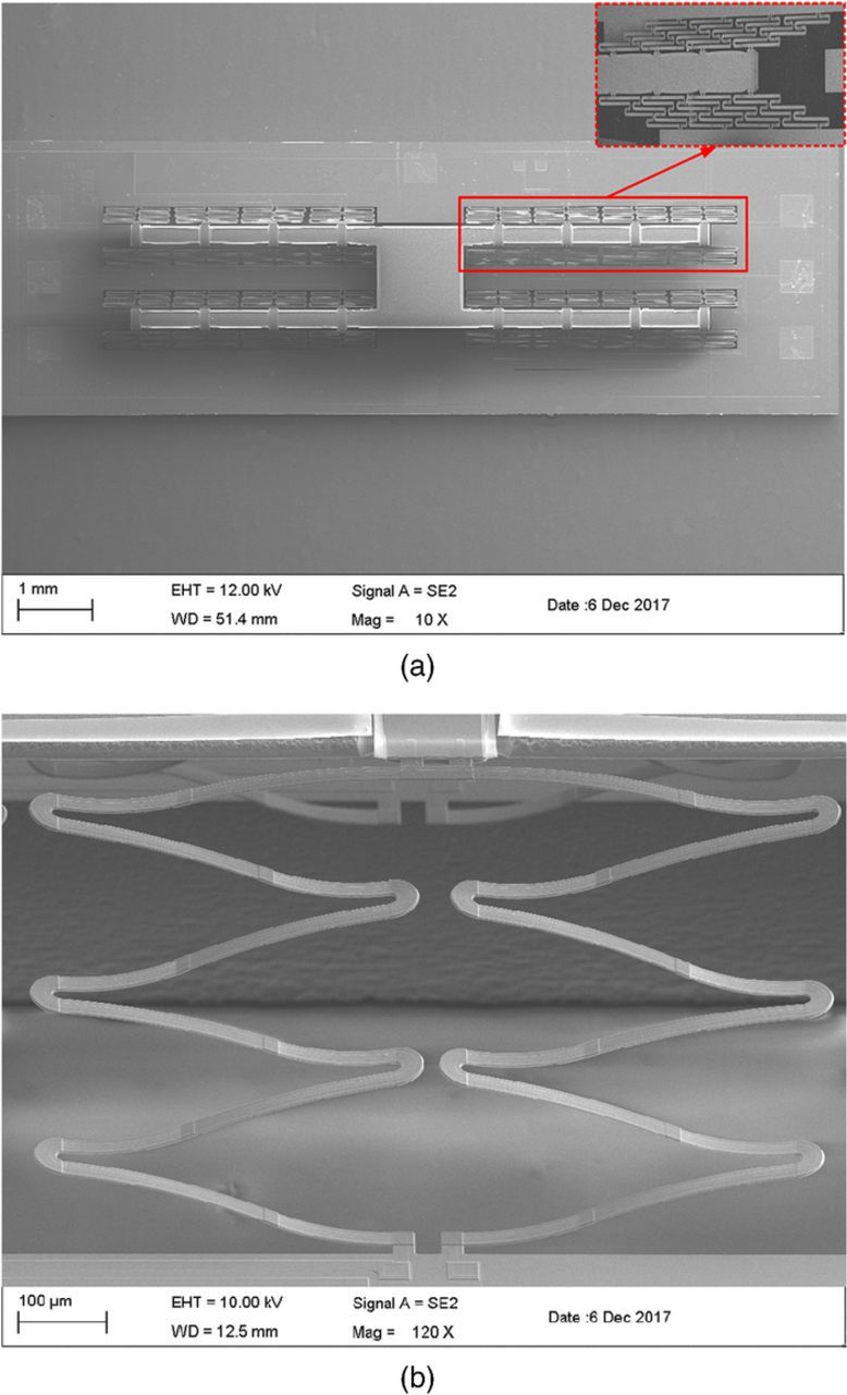
Figure 2. (a) An SEM of a fabricated H-shaped electrothermal MEMS mirror, (b) An SEM of a single pair of three-level DSB actuators.
Characterization of the MEMS mirror has been performed. The measurement results of the static response in piston motion is shown in Figure 3a, where a 406.5 μm vertical displacement is achieved at 9 Vdc. The step response is plotted in Figure 3b, showing the response time is 28 ms. Also, Figure 3c shows the frequency response, where the measured resonance frequency of the first piston mode is 560 Hz.

Figure 3. (a) Static response in piston, (b) Step response in tip-tilt mode, (c) Frequency response in tip-tilt mode.
The thirty-two pairs of actuators are electrically connected into four groups. The resistances of the four groups of the employed MEMS mirror are 191 Ω, 190 Ω, 189 Ω, and 191 Ω, respectively. The small resistance difference is due to fabrication process variations that also produce small differences mechanically among the four groups of actuators. As a consequence, the mirror plate will have a small tilting during its vertical piston scanning when the same voltage is applied to all four groups of actuators. Figure 4 shows the tilt angle versus the vertical displacement. It can be seen that the maximum tilt angle is 0.029° at a large 195.4 μm linear displacement.

Figure 4. Tilt angle versus the vertical displacement.
Design of the FTS Enabled by the H-shaped MEMS
As the MEMS mirror is dual reflective, i.e., both surfaces of the mirror plate are coated with Al for high reflectivity and also optical accessible, two Michelson interferometers are constructed on the two sides of the mirror plate respectively: one for generating sample signals and the other for measuring the position of the mirror plate in real time, as shown in Fig. 5a.

Figure 5. (a) Dual-Michelson interferometer. (MM: MEMS mirror, FM: Fixed mirror, PD: Photodetector, RL: Reference laser, SL: Sample light), (b) Optical simulation of the sample arm.
The optical design of the sample arm is shown in Figure 5b. The sample light is collected by an optical fiber (Ø 600 μm, NA = 0.22) and collimated by two convex lenses. After that, the sample light is split into two light beams by a cubic beam splitter, one to a fixed mirror and another to one side of the MEMS mirror. The two light beams reflected respectively from the fixed mirror and MEMS mirror are combined by the beam splitter and then focused by two convex lenses on a photodetector (PD). The PD picks up the interferogram signal formed by the interference of the two reflected light beams. As the size of the mirror plate is 1.4 mm × 1.2 mm, the light from the sample must be directed to the mirror plate at a spot diameter less than 1.2 mm. Meanwhile, the photosensitive area of the PD is 1 mm in diameter, so the light spot at the PD surface must have a diameter less than 1 mm. After multiple iterations of optical simulation, the four lenses are designed as follows: all four lenses are made of N-BK7 and have a diameter of 6 mm; Lens 1 has a focal length of 9.6 mm while all other three lenses have the same focal length of 11.6 mm. Optical simulation shows that with these lenses and the arrangement shown in Figure 5b the light spot diameters are 1.0 mm at the MEMS mirror and 0.8 mm at the PD, which meet the optical beam size requirements. An InGaAs PD with a spectral response range of 500–2600 nm is chosen for this MEMS FTS.
The system design of the MEMS FTS is illustrated in Figure 6. A Halogen lamp is used as the broadband light source covering both the visible and near infrared spectral range. The sample is illuminated through two modes: diffuse reflection mode and transmission mode, according to the specific application need. In addition to the sample light, a 1310 nm laser is introduced as reference light for spectrum calibration to overcome variable velocity of the mirror, and the interferogram of the reference light path was picked up by another InGaAs photodetector with the spectral response range from 500 nm to 1700 nm.

Figure 6. The system design of the MEMS FTS.
For this FTS system, the theoretical spectral resolution, Δσ, is given by Equation 1:
![Equation ([1])](https://content.cld.iop.org/journals/2162-8777/7/7/Q3025/revision1/d0001.gif)
where ΔZmax is the maximum scanning displacement of the MEMS mirror, ΔD is the optical path difference (OPD). That means the theoretical spectral resolution is inversely proportional to the scan displacement of the movable micromirror. If the MEMS scans 200 μm, the actual OPD produced in system for FFT spectral reconstruction is 165 μm, so the theoretical spectral resolution is 60.6 cm−1. The spectral resolution in terms of wavelength, Δλ, is calculated by Equation 2:
![Equation ([2])](https://content.cld.iop.org/journals/2162-8777/7/7/Q3025/revision1/d0002.gif)
where λ is the wavelength. If a light source of 1,310 nm is used, the resolution will be 10.4 nm.
As shown in Figure 6, electronics are needed to provide drive signals, signal amplification, data acquisition, signal synchronization, and data transmission. The operation is as follows. A digital signal of 5 Vpp at 5 Hz is generated by a microprocessor and converted into an analog signal via a digital-to-analog converter (DAC) that is then conditioned by a power amplifier to actuate the MEMS mirror. A trans-impedance amplifier is needed to convert the photocurrent of the PD to a voltage signal that is subsequently converted to a digital signal via an analog-to-digital converter (ADC). Then this digital signal is transferred into a PC via a USB cable. This digital signal is the interferogram that is transformed into a spectrum and displayed on the PC.
Experimental Results and Discussion
A MEMS based FTS system has been built. A photo of the device is shown in Figure 7a. It measures 29 cm × 19 cm × 11.5 cm (the sample light source not included). Figure 7b presents the MEMS-based Michelson interferometer module with the size of 15 cm × 11 cm × 4.5 cm. The MEMS mirror is driven by a 5 Hz, 0–5 V triangular signal, resulting in about 200 μm scan range. The dual-interferometer module produces two raw interferograms, as shown in Figures 8a and 8b. Since the optical paths in the two arms of either Michelson interferometer are not identical mainly due to the imperfection of the cubic beam splitter and some optical misalignment, the dispersions of different spectral components are slightly different in the two arms. Thereby, either interferogram is not symmetric about its center. For the sample interferogram, that means there is no single highest peak at the center. For the reference interferogram, due to the variable velocity of the MEMS mirror, the frequency of the interference signal is not uniform. Thus, data processing is needed to correct the phase of the interferogram before it can be used for correlating with the sample interferogram to recover the spectrum of the sample light.

Figure 7. (a) MEMS-based FTS, (b) MEMS-based Michelson interferometer module.

Figure 8. (a) The raw interferogram of the reference light, (b) The raw interferogram of the sample light from polystyrene.
Before the phase correction processing, the reference interferogram is applied with finite impulse response (FIR) filtering to suppress noises and a Blackman window to remove the boundary points. Since the reference light is a continuous wave (CW) laser, the reference interferogram is basically a series of fringes and each full fringe corresponds to a distance equal to half of a wavelength of the laser. After the dc component of the reference interferogram is removed, zero crossing and Hilbert transform are used to obtain the instantaneous phase of the reference interferogram. Then the phase is unwrapped and equally divided. After that, the interpolated reference interferogram is used to resample the sample interferogram.20 Figures 9a and 9b show the interpolated interferograms of the reference laser and the sample light from polystyrene, respectively. Before fast Fourier transform (FFT) is applied to the interferograms to recover the spectra, Mertz method is employed to correct the phase.21 Finally, FFT is performed. Figure 10a shows the recovered spectrum of the reference laser, where the measured spectral resolution is 64.1 cm−1, corresponding to 11 nm at 1310 nm, which is slightly larger than the theoretical 10.4 nm resolution. Figure 10b shows the recovered spectrum of the sample light from polystyrene, which agrees with the standard spectrum of polystyrene with a spectral accuracy of 1.5 nm.

Figure 9. (a) The interpolated interferogram of the reference light, (b) The interpolated interferogram of the sample light from polystyrene.

Figure 10. (a) The measured spectra of the 1310 nm reference laser. (b) The measured spectra of polystyrene.
This MEMS FTS has also been applied to measure various liquid samples. Figure 11 plots the measured spectra of N-Hexane, Ethyl alcohol, Gasoline, Aviation kerosene, and Diesel, respectively. All these spectra match those obtained using conventional FTS equipment.22,23

Figure 11. The spectra of several liquid samples, including N-Hexane, Ethyl alcohol, Gasoline, Aviation kerosene and Diesel.
MEMS Scan Stability Study
The stability of the MEMS mirror is crucial for making the MEMS FTS practically useful. There are two types of stability of concern: one is the tilting angle during scanning, denoted as scanning stability, and the other is the initial tilt angle change over time, denoted as long-time stability. To assess the scanning stability and long-term stability of the H-shaped MEMS mirror, a position sensitive device (PSD) is used to measure the tilting angle during scanning while a graph paper that is three meters away from the MEMS mirror is used to monitor the tilt angle when the MEMS mirror is not scanning.
The same 5 Hz, 0–5 V triangular waveform as the one used in the MEMS FTS system was used to drive the MEMS mirrors. Both uncapped and capped MEMS mirrors were tested. Figure 12a plots the measured data for scanning stability testing over 24 hours, where the tilting angles for the uncapped and capped MEMS mirrors were 0.05° and 0.029°, respectively. Figure 12b plots the measured data for initial tilt angle testing over 24 hours. For this experiment, the MEMS mirror was still applied with the triangular waveform but stopped for 10 minutes in every hour. During that 10 minutes, the initial angles were measured. These data show that the initial tilt angles for the uncapped and capped MEMS mirrors were 0.04° and 0.018°, respectively. An uncapped MEMS mirror is a bare MEMS chip that is directly exposed to the air while a capped MEMS mirror is housed in a copper package that is sealed with a glass cover to decrease the disturbances from the environment and to provide an optical window as well. From these experiments, it is obvious that proper packaging can greatly increase the scan stability and long-term stability.

Figure 12. (a) The comparison of the tilting angle during scanning between uncapped and capped MEMS mirrors. (b) The comparison of the initial tilting angle between uncapped and capped MEMS mirrors.
Figure 13 shows the spectra of polystyrene with 10 repeated collections by the MEMS FTS with the MEMS mirror capped. From these data, the calculated wavelength repeatability and accuracy are 0.05 nm and 1.5 nm, respectively, and the baseline repeatability is 0.00037 and spectral repeatability is 0.0009, which are all comparable to the commercial portable spectrometers.24,25

Figure 13. Ten overlaid spectra of polystyrene.
Conclusions
In this work, a novel MEMS FTS system is constructed with a dual-Michelson interferometer architecture enabled by the H-shaped electrothermal MEMS mirror. The MEMS FTS achieves a spectral resolution of 64.1 cm−1, corresponding to 11 nm at 1310 nm. Compared to prior work, this H-shaped electrothermal MEMS mirror has a large scan range of 200 μm as well as high dynamic and static stability with a maximum scan tilting angle of 0.029° and a maximum initial tilting angle change of only 0.018°. Thus, there is no need to use any complex compensation or closed-loop control methods. Another advantage of the MEMS FTS is the wide spectral range of 1000–2500 nm that is only limited by the spectral characteristics of photodetectors and other optical components. For future work, more effort will be spent on developing more robust and lower noise electronics for photodetector and ADC/DAC to increase the system SNR. Meanwhile, more reliable MEMS packaging, more advanced mechanical design and system design will be developed to miniaturize the FTS system without compromising the performance.
Acknowledgments
This work is financially supported by Wuxi Municipal Science and Technology Department (NO. CBE01G1748 and No. 2017YFC0108301).
ORCID
Junyu Chai 0000-0002-3544-5312
Hongzhi Jia 0000-0003-3304-0167