
Abstract
Solid state gas sensors are a core enabling technology to a range of measurement applications including industrial, safety, and environmental monitoring. The technology associated with solid-state gas sensors has evolved in recent years with advances in materials, and improvements in processing and miniaturization. In this review, we examine the state-of-the-art of solid state gas sensors with the goal of understanding the core technology and approaches, various sensor design methods to provide targeted functionality, and future prospects in the field. The structure, detection mechanism, and sensing properties of several types of solid state gas sensors will be discussed. In particular, electrochemical cells (solid and liquid), impedance/resistance based sensors (metal oxide, polymer, and carbon based structures), and mechanical sensing structures (resonators, cantilevers, and acoustic wave devices) as well as sensor arrays and supporting technologies, are described. Development areas for this field includes increased control of material properties for improved sensor response and durability, increased integration and miniaturization, and new material systems, including nano-materials and nano-structures, to address shortcomings of existing solid state gas sensors.
Export citation and abstract BibTeX RIS

This is an open access article distributed under the terms of the Creative Commons Attribution 4.0 License (CC BY, http://creativecommons.org/licenses/by/4.0/), which permits unrestricted reuse of the work in any medium, provided the original work is properly cited.
Sensors are devices that produce a measurable change in output to a known input stimulus. Sensors are also transducers: the incoming stimulus is changed or transduced by the sensor into an electrical or other output for the user. The stimulus can be a physical or chemical stimulus. The output signal is generally proportional to the input stimulus being measured. A given sensor can be described from the target measurement point of view e.g., temperature sensors, or from the platform point of view, e.g., electronic sensors. The emphasis in this paper will be on sensor classes based on their platform and sensing mechanisms.1 Figure 1 shows a possible breakdown of sensor classes based on the energy transduced in the sensor.1 These are radiant, mechanical, thermal, magnetic, electronic, and electrochemical sensors (with the electronic and electrochemical sensor classes combined given their similarities). It also provides examples of specific sensor types in each category. There are a range of sensor types within each category, e.g., within the electronic and electrochemical sensor classes possible sensor platforms include metal oxide semiconductors and electrochemical cells.2
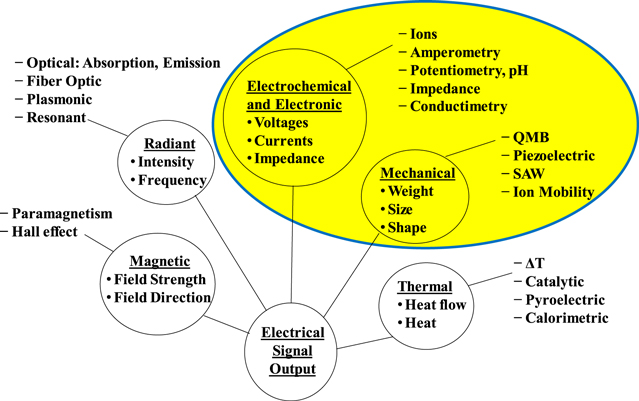
Figure 1. Classes of chemical sensors by transducer platform, with examples of the different sensor types.1 The highlighted section is the general topic of this paper.
Download figure:
Standard image High-resolution imageThis paper addresses chemical sensors that measure concentrations of gas species using "solid state" sensor platforms, whose sensing mechanism involves a reaction of the gas species with the sensing element in the sensing structure, and conversion of that reaction into an electrical signal. As shown in the highlighted region of Fig. 1,1 this paper concentrates on classes of sensors with electronic and electrochemical platforms, and mechanical transduction mechanisms. In particular, this paper discusses electrochemical cells (solid and liquid), impedance/resistance based sensors (metal oxide, polymer, and carbon based structures), and mechanical sensing structures (resonators, cantilevers, and acoustic wave devices). Although of high interest, other sensor types shown in Fig. 1, such as radiant, magnetic, or thermal, in general have different type of sensing structure and mechanisms, and will not be covered in this paper due to length restrictions. Further, this paper will not discuss larger instruments, such as mass spectrometers, or analytical assays, but concentrate on detection of gas species using the transduction mechanisms in the highlighted section of Fig. 1.
An overview of the considerations involved in the applications of gas sensors, and overall field of gas sensor technology will first be given. Then, for each class of solid state gas sensor, this paper will examine the state-of-the-art in multiple sensor technologies with the goal of understanding: 1) The core technology and approaches describing the sensor design and sensing mechanism, and how that mechanism is used to provide a measurement of the ambient gas species; 2) Sensor response based on that core technology, and how it can be modified to provide specific functionality for a given application and gas species measurement with an example structure; 3) Future prospects discussing critical issues, challenges, and future directions in the field for each sensor class. Sensor arrays and supporting technologies will also be described. A discussion on the overall direction of the field of solid state gas sensors related to the sensor types considered will be provided.
Background
This section provides a basic background related to some of the considerations involved in the development and application of chemical sensor technology for gas detection. In summary, for the purposes of this discussion, a chemical sensor provides information related to the chemical species in the environment relevant to a particular application. The range of potential applications for gas sensors is vast. To give a few narrow examples, gas sensors may be used in the detection of: automotive and industrial emissions; fuel leakage in order to avoid explosive conditions; industrial process control; toxic species for personal health; combustion species for fire monitoring; fuel cell monitoring; and many others.
There is not a single sensing class or technology that can effectively detect everything of interest in every possible environment. Rather, selecting the optimum sensing approach from a group of technologies may be the best method to address a sensing need.2 Each chemical sensor platform has its own strengths, ideal range of application, and provides different types of information about the environment. For example, different sensor platforms have different responses to the reactant gas (e.g. exponential, logarithmic, power law, etc.). They may also have different operating temperature range, response to the ambient environment, packaging requirements, etc. Which sensor class, platform, or combination of platforms one uses, and how those sensors are tailored, depends on the needs of the application. Example considerations include:1
- 1.What are the measurement requirements? High sensitivity in a narrow concentration range, or a detection across broader concentration range?
- 2.Can the application needs be met by careful choice of the operating parameters of a given sensor, or will a combination of technologies be needed to sort out the contribution of various similar analyte?
- 3.Does the application's operating environment require special materials or fabrication procedures?
A number of other considerations are relevant. It is important that the sensor designer understands the needs and specifications of the targeted application, and tailors the sensor for the needs of the application.
Four common parameters are typically cited as relevant in determining whether a chemical sensor can meet the needs of an application:3 sensitivity, selectivity, response time, and stability. Sensitivity refers to the sensor's ability to detect the desired chemical species in the range of interest. Selectivity refers to the sensor's ability to detect the species of interest in the presence of interfering gases that also can produce a sensor response. Response time refers to the time it takes for the sensor to provide a meaningful signal (often defined as 90% of the steady state signal) when the chemical environment is changed. Finally, stability refers to the degree to which the sensor baseline and response to a given environment changes over time. Simply stated, one needs a sensor that will accurately determine the species of interest in a given environment with a response large and rapid enough to be of use in the application, and whose response does not significantly drift over its designed operational lifetime.
A major challenge is to find a suitable sensor material(s), which provides the required sensitivity, selectivity, response time, and stability for the targeted application. Achieving such capabilities often requires tailoring of the sensor structure to optimize its use for a given detection problem. For example, the platform for an electrochemical cell to detect gases can be formed and repeatedly fabricated. However, varying the selection of electrolyte and electrodes to be deposited in the sensor structure can result in very different gas sensor types. Figure 2 shows an example of this approach with, in effect, a family tree of sensor platforms and the wide range of sensor types and measurement options, which can result from using these platforms.2 Each chemical sensor platform has its own strengths, ideal range of application, and provides different types of information about the environment. For example, different sensor platforms have different responses to the reactant gas (e.g. exponential, logarithmic, power law, etc.). Which sensor class, platform, or combination of platforms one uses, and how those sensors are tailored, depends on the needs of the application. Figure 2 is just one example and many variations to this approach can be envisioned.
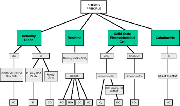
Figure 2. An example electronic and electrochemical gas sensor platform technology family tree. Given a limited number of platforms, a wide range of gases can be detected. Several platforms are shown and example target detection species are noted for a configuration of the platform.2
Download figure:
Standard image High-resolution imageIt is often the case, that a single sensor will not meet the needs of the application, and thus the need for a sensor array for a fuller field measurement. Further, supporting technology is often core to enabling a sensor element to provide the required data in a given application. An example of an approach to this is a "Smart Sensor System."4 The definition of a Smart Sensor may vary, but typically at a minimum a Smart Sensor is the combination of a sensing element with processing capabilities provided by a microprocessor. That is, Smart Sensors are basic sensing elements with embedded intelligence. The sensor signal is fed to the microprocessor, which processes the data and provides an informative output to an external user. A complete self-contained sensor system that includes the capabilities for logging, processing with a model of sensor response and other data, self-contained power, and an ability to transmit or display informative data to an outside user. The fundamental idea of a smart sensor is that the integration of silicon microprocessors with sensor technology, can not only provide interpretive power and customized outputs, but also significantly improve sensor system performance and capabilities. Such technologies can provide augmentation to the capabilities of gas sensor elements or arrays.
The following is a review of how such challenges were met for a range of applications based on the transducer platforms and sensor types highlighted in Fig. 1. Even with the narrowing of the topics in this review suggested by Fig. 1, the overall topic is still very large. This review will not cover each topic in extensive detail, but will rather give illustrative examples of sensor technologies in a given class and sensor type. Each section will examine a different sensor class and for each sensor type generally describe as appropriate:
- 1.The core technology on which the sensing approach is based
- 2.Sensor design and detection mechanisms
- 3.Sensor Example including response and example structure
- 4.Future Prospects: This includes Problems, Critical issues, Challenges, Possibilities, and Future Directions in the field for each sensor class.
Given the wide variety of topics chosen, this outline will vary, but these topics will be generally addressed. The sensor topics discussed are:
- Electrochemical Cells
- Electronic Metal Oxides
- Conductive Polymers
- Carbon Based
- Carbon Nanotube Based
- Graphene Based
- Resonators and Mechanical Based
- Sensor Arrays
- Complimentary Technologies: Microfluidics
Sensor Classes
Electrochemical cells
Core technology
Electrochemical-based sensors have been used extensively in chemical and biochemical detection. In this section, the discussion focuses on the gas detection. Specifically, solid and liquid phase electrochemical sensors for the gas detection will be discussed.
An Electrochemical sensor is an electrochemical cell. It contains either a two-electrode or a three-electrode configuration, and an electrolyte. In the two-electrode system, the sensor contains a working (sensing) and a counter (reference) electrode. In the three-electrode system, the counter and the reference electrodes are separate, and the sensor contains working, counter, and reference electrodes individually. The ion conductive electrolytes can be liquid phase or solid phase providing the proper classification of the electrochemical sensors.
An Electrochemical sensor combines an electrochemical recognition mechanism and an electrochemical transduction mechanism. The electrochemical recognition mechanism is an electrochemical reaction occurring at the surface of the working electrode, and this reaction can be either an oxidation or a reduction reaction making the working electrode an anode or a cathode, respectively. Consequently, the counter electrode will then be the cathode or anode, respectively as well. This electrochemical reaction occurring at the surface of the working electrode is governed by the thermodynamically well-established Gibbs free energy relation, where Gibbs free energy change of the overall reaction in the cell is equated to the negative of the electrical work:

where, ΔG is the Gibbs free energy change; n is the number of electrons transferred; F is the Faraday constant; and ΔE is the open-cell potential. Thus, the electrochemical reaction will only occur at the working electrode surface when the value of –ΔG of the specific reaction is reached.
The electrochemical transduction mechanism converts the result of the electrochemical recognition reaction into an electrical output quantifying the activity (or concentration) of the detecting species in the electrochemical reaction on the working electrode surface. In general, this electrochemical transduction mechanism assesses the relationship of the electrochemical potential and its electrochemical current derived from the recognition reaction. Many electrochemical analytical techniques can be used for this transduction mechanism, such as conductivity measurement, coulometric analysis, electrochemical impedance spectroscopy (EIS) and others. For the electrochemical sensors discussed, we will focus on the most commonly employed electrochemical transduction mechanism: potentiometric and amperometric measurements.
Sensor design and detection mechanism
Potential-based electrochemical sensor is a Galvanic cell in which the electrical current is produced spontaneously by the electrochemical reaction occurring at the working and reference electrode surfaces. Under quasi-thermodynamic equilibrium condition, Nernst equation is applicable:
where, E is the measured electrochemical potential, E0 is the electrochemical potential at the standard state, R is the gas constant, T is the absolute operating temperature in Kelvin, F is the Faraday constant, aoxi is the activity of the oxidation form and ared is the activity of the reduction form of the relevant species. For an electrochemical sensor, the above Nernst equation can be modified as:

where, ameasured is the activity (concentration) measured of the relevant species, and areference is the activity (concentration) of the relevant species at a reference state. This equation demonstrates that a linear relationship exists between the measured electrochemical potential, E, and the natural logarithm of (ameasured/areference). If areference is known or fixed, then the potential, E, can be related to the natural logarithm of ameasured linearly with a slope of (RT/nF). This is the fundamental basis of an electrochemical sensor.
Amperometric–based electrochemical sensor assesses the potential-current relationship. An electrochemical potential (vs the reference or counter electrode) is applied to the working electrode generating an electrochemical reaction of the selected, relevant species on the working electrode surface. This reaction yields a current, which is directly related to the quantity of the species involved. This current produced is linearly related to the bulk concentration of the selected species providing a more sensitive measurement to the selected species as compared to the natural logarithm value of the selected species in a potential–based electrochemical sensor. However, both material transfer and chemical kinetics are involved and interwoven in the measurement of an amperometric electrochemical sensor. Therefore, careful analysis and assessment of all contributing factors of the measurement are required.
Electrochemical based gas sensors are used extensively in many practical applications. These include process control industries, environmental monitoring, fire detection, harmful gases detection in mines and home safety. It will not be feasible for introducing every gas sensor for each application. We will instead choose a specific sensor for the illustration of electrochemical-based gas sensor demonstrating the general operating principle.
Sensor response and example structure
Measuring oxygen in gas phase is common and is important in many practical applications. Oxygen gas sensor is a typical electrochemical system. It consists of a working, a counter (reference) electrode, an electrolyte and a container. This is a standard two electrode sensor system. A three-electrode configuration system is also feasible. It contains a working, a counter and a reference electrode. In this three-electrode configuration, electrochemical potential is applied between the working and the reference electrode based on the Gibb's free energy theoretical assessment as described above. The corresponding current output is measured between the working and the counter electrode. In this arrangement, any increase or change of resistance in the electrolyte at the interface of working electrode and the electrolyte due to the electrochemical reaction at the working electrode can be overcome by increasing the applied potential between the working and the reference electrode maintaining the suitable Gibb's free energy for the completeness of the electrochemical reaction occurring at the surface of the working electrode. The increase of applied potential can be accomplished electronically. Consequently, this results in accurate detection for the sensor using this mode of operation. The commonly used amperometric sensor is based on this approach.
Oxygen reduction reaction (ORR) occurred at the cathode of an electrochemical system is an important reaction for oxygen sensing and electrochemical energy storage system. It is recognized that oxygen reduction in aqueous solution occurs mainly through two different pathways: a four electron transfer from O2 to H2O or a two electron transfer from O2 to H2O2.
ORR can take place in an alkaline or acidic medium. In an alkaline medium, the ORR vs a reversible hydrogen electrode (RHE) at 25 °C and its electrochemical potential at standard state for the 4-electron transfer are:

For the two electron transfer, involving H2O2:


In the acidic medium, the ORR vs a reversible hydrogen electrode (RHE) at 25 °C and its electrochemical potential at standard state for the direct 4-electron transfer is:

And the indirect reactions are:


Thus, regardless of the kinetic mechanism of oxygen reduction, it is clear that oxygen can be electrochemically reduced at the cathode in either an alkaline or acidic aqueous medium.
However, the reaction kinetics at the cathode of an electrochemical system including an oxygen sensor is slow due to highly irreversible ORR. Consequently, electro-catalysts are introduced in order to enhance the reaction kinetics and the sensing time. These electro-catalysts consist of single metal, bi-metallic alloy and transition metal catalysts, as well as metal oxides and nano-structure catalysts. However, the discussion of the functions of these catalysts is beyond the scope of this presentation.
For an oxygen sensor, in addition to the employment of proper electro-catalyst, it also involves a thin, semi-permeable membrane. This membrane is placed in front of the oxygen sensor allowing the oxygen in the test sample diffuse across the membrane at a rate proportional to the pressure of the oxygen in the aqueous test sample. The diffused oxygen is then reduced at the cathode producing an electrical current which is directly related to the concentration of the oxygen in the test sample. Thus, the membrane not only defines the oxygen diffusion rate to the cathode, but also separates and minimizes any other species in the sample to reach the cathode enhancing the selectivity of the oxygen sensor.
We use the oxygen gas sensor with a liquid phase electrolyte to illustrate the general operation of an electrochemical-based gas sensor. Fundamentally, we use either a two or a three-electrode configuration. Based on the gas to be detected or measured, either an oxidation or a reduction reaction will take place at the interface of the electrolyte and the working electrode surface. Consequently, an applied electrochemical potential can be identified based on the Gibb's free energy assessment. The choice of the electrode material, configuration and size can be determined based on the specific needs and requirement.
In addition to liquid phase electrolyte, electrochemical-based gas sensors can also use solid phase electrolyte. In view of the limited scope of this article, we will focus the discussion on the solid electrolyte based oxygen sensor. Also, coverage of this topic in existing literature is extensive, and the discussion will be specifically focused on the technological challenges and the future research opportunities after a brief description of the operation principle. For further reading, the readers are directed to additional references.5–7
The so-called Type I oxygen sensor typically uses yttria-stabilized zirconia (YSZ) as a solid electrolyte and measures the unknown oxygen partial pressure with respect to a known partial pressure that is created by sealing air (21 mole % of oxygen) on the reference side. The interface potential is established by the local equilibrium reaction ( ); referred to as the oxygen reduction reaction (ORR) occurring at the electrode/electrolyte/gas triple-phase boundary (TPB). The measured signal is proportional to the logarithm of the ratio of the two partial pressures. In automotive application, the sensor signal varies by several orders of magnitude for slight deviation from the stoichiometric air/fuel mixing ratio, thus works as a switch and help maintain the stoichiometric mixing for optimum combustion. This type of sensor is inherently selective since the detecting species (O2) is the same as the transporting species in the electrolyte (O2− conductor). However, this sensor has its own limitations. First, maintaining a gastight seal for the air reference at high operation temperature of ∼800 °C is a challenge. Much research conducted in this area leads to the development of high-temperature ceramic sealant. Second, since the signal varies logarithmically to the partial pressure ratio, this sensor is not useful for monitoring continuous change in oxygen partial pressures, particularly in the high-pressure range.
In order to overcome these limitations, an amperometric oxygen sensor (also called limiting-current-type sensor) was developed where the working electrode of the zirconia cell has a pumping electrode inside an enclosure containing a small aperture or diffusion hole. When the electrode inside the enclosure is negatively biased, oxygen molecules are reduced at the cathode to form oxygen ions, which are then pumped to the anode outside the cell. The sensor is operated in a voltage range where the current reaches a steady state, which is determined by the rate of arrival of oxygen from the ambient through the hole to the working electrode. The pumping current at steady state depends linearly on the oxygen partial pressure in the ambient. Sometimes this sensor is called "a proportional oxygen gauge," adopted to monitor lean-burn automobile engines.
Future prospects: problems and possible solutions
Depending on the size of the aperture, the diffusion of gas can be characterized as a bulk diffusion process or a Knudsen diffusion process. Bulk diffusion occurs when the aperture diameter d is much greater than the mean free path λ of the gas molecules, such that the frequency of molecule-wall collisions is negligible compared with intermolecular collisions in the free space. At atmospheric pressure, this corresponds to the hole diameter greater than about 105 Å. For small channel (less than ≈ 100 Å) where  gas diffuses by Knudsen diffusion whose coefficient
  is one to two orders of magnitude smaller than the bulk diffusivity,
  This limit is typically exhibited in coating/diffusion barrier prepared by the sol-gel process.6 For an intermediate pore radius (102–105 Å), a mixed diffusion behavior is expected, with the resulting diffusivity of
  For the bulk diffusion and Knudsen diffusion limits, the sensor signal (limiting current) can be related to the oxygen content by simple linear relations.2 With aging, physical modification of the diffusion barrier can cause signal deterioration. So, new materials and methods need to be developed for the long-term durability of the limiting current amperometric sensors.
The oxygen sensor measures the oxygen partial pressure for the equilibrium electrochemical reaction occurring at the sensing electrode, ORR. However, when the concentration of oxygen in an exhaust gas containing various reducing species is measured, the response is often affected by competing chemical reactions involving CO, NOx and HCs. The kinetics of these reactions depend on temperature and the electrode materials. For example, at high temperature (>600 oC), ORR is generally far faster than the other reactions, which are relatively fast on highly catalytic electrodes such as Pd, Rh and Pt and slow on low-catalytic electrodes such as Au. Hence, when Pt is used as a sensing electrode for the zirconia oxygen sensor, it does not measure the oxygen content existing in the non-equilibrium exhaust gas, but rather the oxygen concentration that the exhaust gas would have if it were in the internal thermodynamic equilibrium. When low-catalytic sensing electrodes are used, they measure the actual oxygen content in the non-equilibrium exhaust gas due to the negligible extent of chemical reaction at the electrode surface. At moderate temperature (500 oC–600 oC), where the rates of the other reactions are comparable to that of the ORR, the steady cell voltage responds to the mixed potential established by the competing reactions. Mixed potential sensors are a much discussed topic in literature,8,9 and is beyond the scope of this article.
Another idea to replace the air reference with a metal/metal oxide internal reference has been extensively explored. Fouletier et al.10 demonstrated that a metal/metal oxide mixture encapsulated within a ceramic superstructure and placed in intimate contact with Pt would generate a fixed oxygen partial pressure at a given temperature. However, failure to achieve gastight sealing limited the application of these internal reference based sensors. Seeking to improve on the sealing, Haaland11 proposed that it would be possible to hot press a gastight Pt/zirconia chamber into which a known oxygen concentration can be pumped. Expanding around this idea, Dutta-Akbar group12 was able to seal a metal/metal oxide reference chamber by a high pressure (3–6 MPa) and high temperature (1200 °C–1300 °C) bonding method that exploits grain boundary sliding creating ceramic joints that are pore free. Pd/PdO-based internal reference oxygen sensor manufactured by this method showed very stable sensing responses over repeated cycles and extended periods up to 800 °C.12 Further R&D in this grain boundary sliding promoted bonding may present a viable method for gas tight sealing that is central to high temperature sensors and fuel cells.
Electronic metal oxides (DC and AC measurements)
Core technology
Resistive-type metal oxide gas sensors (MOGS) are generally low-cost, low-power, portable and highly stable but primarily suffer from poor selectivity and require complex algorithms to analyze an integrated array of sensors to reliably detect just a few gases. Efforts to enhance the selectivity of the materials used in the sensors could greatly reduce the complexity of the integrated sensor arrays. The most promising method of increasing selectivity in MOGS is to mix the primary metal oxide sensing material with another metal oxide, noble metal catalyst, polymer or carbon nanotubes.13–15
The sensing mechanism in MOGS relies on the exchange of electrons between the analyte gases and surface of sensor material via chemisorption or catalytic reaction. The changing charge carrier concentration can be measured simply as a resistance change vs time when the sensor material creates a current path across an electrode gap. However, the dominant mechanisms causing the resistance change can become complex when incorporating multiple n-type, p-type and catalytically active materials. The depletion layers formed at the interfaces and the surface redox reactions can be modified in several ways by tuning the composition, dispersion and morphology of the constituent sensor materials. Complex hierarchical nano-heterostructures have been designed to incorporate several active sensing materials in a well-defined form that optimizes electron/hole exchange and movement. Others have focused on tuning doping levels and composition of fine mixtures of nanoparticles toward the catalytic reaction pathways occurring at the surface. Many have taken a combinatorial approach toward empirically finding the optimal mixtures and more still simply evaluate the sensor properties of any new nano-heterostructure they can synthesize. This has created a situation where new nano-heterostructures have been created much faster than they can be understood. For resistive-type MOGS to break through the selectivity disadvantage over a wide range of applications, the mechanisms behind the observed improvements must be better comprehended. This section focuses on strategies for designing nano-heterostructures and state-of-the-art methods for characterizing their sensor behavior. Topics beyond the scope of this review is low temperature (room temperature) sensing by light-activated MOGS-based sensors or system on chip integration.16,17
Sensor design
With the countless new nano-heterostructure designs emerging, researchers have continually found that the dispersion of the constituent sensing materials in the nano-heterostructures is as important as the composition itself. A bi-layer thin film of two oxides is the extreme example of no intermixing and a well-defined interface.18 A sensor could also mix nanoparticles of the same two oxides into a single-layer thin film to increase the number of interfaces between dissimilar materials.19 Further, the particle sizes of the two oxides could be adjusted so that one is small enough to decorate larger particles of the other.20 The core particles could also be nanowires,21 and the decorative particles either discrete22 (not touching each other) or form a continuous shell.23 This design can also take the form of hollow nano-spheres24 or brush-like structures utilizing nanorods for decoration,25 and any of these can further be decorated with noble metal nanoparticles.26 All the above examples could be synthesized with the same two or three binary oxides and yield wildly different sensor properties.
To choose a design, one must consider the role of each material in the sensor function. Which material has the highest catalytic activity toward the gas? Which is the most morphologically stable? Should the core or decorative particles have a depletion or accumulation layer? Does the primary gas need access to both materials? Can a reaction product from interaction of the first material interact further with the second material? Through which material should the current flow, and can its resistance modulation be easily measured? In many cases, answers to these questions are not well founded because of lack of systematic studies.
Rapid progress in new synthesis routes has made it possible to engineer and optimize specific types of nano-heterostructures for a given application. However, the largely trial-and-error approach has failed to effectively understand and model the response behavior of these nano-heterostructures in a way that could otherwise advance the field toward bottom-up design for specific applications. The now widespread approach to developing new sensor materials involves a new synthesis method or new mixture of materials into a nano-heterostructure followed by standardized testing toward every gas available in the laboratory and publishing the results of the tests. There are very few attempts to investigate why the new heterostructure is an improvement over existing materials. The results are inconsistent across different laboratories and it is nearly impossible to draw fundamental conclusions by assembling results from different sources. There is a clear need for a more fundamental approach to understand the role of defect states, band edge alignment, charge carrier concentration, interfaces and charge conduction pathways in nano-heterostructures.
Sensor examples
One of the simpler approaches that has proven effective is to use combinatorial methods and high-throughput testing to rapidly assess a range of compositions and particle sizes optimal for given test conditions.27 In many cases, the performance drops off quickly, more than a few percent away from the optimal composition. However, it is difficult to untangle the effects of morphology and composition when these are often co-dependent during synthesis. In more complex nano-heterostructures, Woo et al.23 showed that discrete Cr2O3 nanoparticles on ZnO nanowires had a much greater n-type response toward trimethylamine (TMA) than if Cr2O3 formed a continuous shell giving a p-type response. It was found that the continuous p-type shell confined the current flow primarily to the shell and limited the interaction with the core ZnO nanowires. Kim et al.28 more recently showed that finely intermixed nanoparticles of Cr2O3/ZnCrO4 forming hollow nanospheres synthesized via galvanic replacement exhibited much higher selectivity and sensitivity toward part per million (ppm)-level xylene than pure Zn, Cr2O3 and ZnCr2O4 powders or a coarse mixture of Cr2O3 and ZnCrO4 powders. They suggest that reaction intermediates formed by one compound can further react with the other, and minimizing the distance between nanoparticles of the two compounds maximizes the reaction rate. Other studies have shown there to be optimal diameters of the decorated particles or continuous shell for a given gas analyte and operating condition. One incredibly effective combination is CuO nanoparticles decorated on a stable oxide nanowire for H2S sensing.29–31 If the CuO diameter is small enough, it can fully and reversibly phase change to CuS in the presence of H2S causing a massive change in conductivity from semiconducting to semi-metallic. If these nanoparticles form a junction through which current is forced to flow, they can act as a resistance "switch" with high selectivity and sensitivity. This principle can also be applied to semiconducting oxide nanoparticles undergoing depletion of charge carriers without a phase change. Choi et al.32 utilized atomic-layer deposition (ALD) for precise processing control of continuous ZnO shells on SnO2 nanowires. They synthesized a range of shell thicknesses and found 40 nm to be optimal for sensing of reducing gases.
In resistive-type sensors, the baseline resistance value can influence the magnitude of the sensor response and thus overall performance. As sensors are shrinking to fit into integrated circuits using MEMS technology, it is important to consider the effects of the electrode architecture on the performance of the sensor materials. For example, Song et al.33 examined four electrode designs and found that a smaller electrode gap area produced a higher response in In2O3 thin films and nanorods to 50 ppm ethanol at 300 °C, primarily due to the increase in the baseline resistance. Similarly, Vallejos et al.34 found that a 5 μm electrode gap showed a 32-fold faster response toward H2 and better overall stability compared to a 15 μm gap using Pt-functionalized tungsten oxide nanowires of 10 μm average length. A useful follow-up study would be to use nanowires of varying controlled lengths and varying electrode distances to assess any relationship between nanowire length and optimal electrode gap. Smaller sensing areas utilizing less sensor materials also allows for the oxides to be self-heating if the applied current or voltage is high enough and power dissipation can be properly managed. The current can be pulsed to further minimize power consumption and prevent overheating.35 This creates an exciting possibility for miniaturized portable sensors using only μWatts of power.36
Future prospects: critical issues, challenges, and future directions in the field
To understand how these complex nano-heterostructures interact with the gas atmosphere, we must first understand the physical and electrical properties of the structures themselves. Careful electrical measurements on well-defined nano-heterostructures will be paramount in understanding the underlying mechanisms. Single-nanowire measurements,37,38 have shown promise due to their measurable, well-defined shape and size and possibility of direct imaging and elemental mapping of the dispersion of secondary sensor material. A known geometry allows resistivity measurements in various atmospheres, which can provide a direct comparison of resistivity responses between several candidate compositions or dispersions. These types of measurements further enable modeling of depletion layer changes. However, this approach includes many pitfalls, which must be accounted for that may otherwise invalidate the data. For instance, the electrode-semiconductor interface resistance may be comparable to that of a single-crystal nanowire and this potential energy barrier may dominate the response curves. Some groups have used a 4-probe approach to measure the contact resistance in a single nanowire sensor as a function of temperature to determine when the measurements are valid.39 The electrode metal(s) should be chosen such that the Fermi energies are closely matched to the semiconductor to minimize the contact resistance. Unfortunately, Focused Ion Beam (FIB) deposition sources are often limited to Pt with Au and Ti sources quite rare. This configuration also places noble metals in close proximity to all of the active sensing material and can act as an artificial catalyst toward some analyte gases. Extended direct current voltage biasing may also cause lattice diffusion or drift of charged defects that becomes significant on this size scale. To minimize the effects of contact resistance and charged defect drift, several groups have explored alternating current (AC) electrical measurement and analysis referred to as impedance spectroscopy.40 This technique has been well-developed over several decades in ceramic electrolytes and semiconductors, but is only recently being applied to nanomaterials. When the physical system is appropriately modeled with an equivalent circuit, the resistance and capacitance contributions of each mechanism can be tracked through varying gas atmospheres and temperatures.41,42 These measurements may even be capable of showing varying relaxation times across the heterostructure interface due to defect states present. Understanding the electrical properties at this depth will aid in design of nano-heterostructure sensors with optimized performance.
Complex synergistic reactions can be studied by analyzing the downstream reaction products using a flow-through FTIR or dedicated catalytic experiments using a GC-MS. Once the reaction pathways near the surface are understood, the operating temperature and relative composition of the synergistic materials can be tuned by measuring the un-reacted analyte gas to maximize the reaction rate at the surface, thus enhancing the sensor response and/or selectivity.43 Additionally, some researchers have focused on the transients in the sensor response/recovery curve where introduction of an analyte gas quickly yields a new baseline resistance but shows a small but reproducible drift to a higher or lower resistance. This can be a result of a slower or secondary reaction whose behavior may change with temperature.44 This mechanism can be differentiated from drift caused by morphological changes if the above-mentioned flow-through FTIR is used to analyze the reaction products as a function of time.
As materials are being combined in ever-shrinking sizes and more intricate hierarchical designs, they become more challenging to properly characterize. Fortunately, recent advances in instrumentation have provided new state-of-the-art techniques where the physical, electrical, and even optical properties can now be measured with a spatial resolution of a few nanometers. Direct measurement of these properties helps to refine models of mechanistic behavior, which will guide future design of nano-heterostructures.
One such technique is cathodoluminescence (CL). CL has been well-developed in a scanning electron microscope (SEM) but has recently been incorporated into a scanning transmission electron microscope (STEM) through custom-built hardware and is now commercially available. Principally, cathodoluminescence operates by exciting electrons in the semiconductor and collection of the emission spectrum from their recombination across the band gap or into various defect states. SEM-CL is capable of both time-resolved and depth-resolved emission collection,45 and can use a low-energy beam to preferentially probe surface states at a spatial resolution useful for nano-heterostructures. STEM-CL can probe surface states via a beam probe at the edge of a nanoparticle and bulk defect states by probing the thicker regions with a transmitted beam.46 Korotcenkov et al.47 showed that the defect states in SnO2, as measured by CL, have a direct correlation to the resulting sensor properties. The CL emission spectrum can act as an indicator for process variations in crystal size, defect concentration and dopant levels. Perhaps the most significant advantage of STEM-CL over SEM-CL is that it can simultaneously utilize the entire suite of analytical electron microscopy tools present on a microscope to collect crystal orientation, elemental mapping, local bonding environment, and dielectric properties all on a single nanoparticle.48 The interfacial band bending often cited as a determinant mechanism for unique or improved sensor behavior is rarely measured. X-ray photoelectron spectroscopy has shown promise in measuring Fermi energy, conduction band and valence band offset in nano-heterostructures in vacuum.49–51 Specialized environmental XPS instruments may now make it possible to measure these offsets as a function of temperature and gas atmosphere, although the atmospheric composition choices may be limited.
To understand the underlying causes for enhanced selectivity using these nano-heterostructures, the structures themselves must be better understood. This depth of electronic, optical and chemical characterization will be essential for advancing the field toward bottom-up design of nano-heterostructures toward specific applications. Improvements in sensor characteristics (response and selectivity) are often credited to two mechanisms termed electronic and chemical sensitization. Where electronic sensitization describes free carrier exchange due to Fermi level equilibration, chemical sensitization describes enhanced gas-surface interactions. Three review articles have recently been published each of which focuses on different aspects of these sensitization mechanisms. The first of these articles discusses the synergistic effect electronic and chemical sensitization has on improvements in sensitivity and selectivity.52 The second article discusses how decorated and core–shell nanowire sensors can improve response magnitude due to Fermi level equilibration.53 The third discusses the role of defects, oxygen vacancies in particular, in both the interior and the surface of metal oxide sensing materials which controls both bulk electronic behavior and surface interactions.54
Conductive polymers
Core technology
Conducting polymers (CPs) is a class of organic materials and are promising for various applications including gas sensors. The interest in CPs as useful materials was initiated in 1977 when Heeger, MacDiarmid, and Shirakawa demonstrated that the conductivity of polyacetylene can be increased by 9 to 13 orders of magnitude, after an oxidation process (doping) with iodine.55 These primary experiments, for which the three scientists were awarded the Nobel Prize for Chemistry in 2000, produced a great interest in CPs. The conduction of these types of polymers is due to conjugation in the backbone of the polymer.56,57 The molecular arrangement of CPs consists of alternate single and double bonds, which allows the formation of π-electrons partially delocalized across a few atoms of the polymer system. This electronic delocalization provides the "highway" for charge mobility along the backbone of the polymer chain. The bond alternation combined with the consequent restriction on the extent of the delocalization leads to the formation of energy gap. Some CPs generally exhibit semiconductive to insulating levels of conductivity in their pristine state but can be raised to metallic levels by doping with suitable species.58,59 Doping, in this case, refers to the oxidation (removal of some delocalized electrons) or reduction (addition of electrons) of the π-electronic system which makes the CPs p-type and n-type semiconducting materials, respectively. Most of the CPs are p-type semiconductors, as anion dopants induces positive charges across several monomers. To maintain electro-neutrality, doping of conducting polymers requires the incorporation of a counterion. In some cases, the conductivity can be introduced by adding external ingredients (e.g., carbon black/metal oxides or metallic fibers).60,61 CPs can be used as the selective responsive layer in gas sensors, or as a transducer itself. Thus, for example, conductance change of a CP on exposure to a gas is the sensing mechanism in a chemiresistor. Likewise, conductivity change in a CP can be used as interconnect of flexible devices.62,63 This section will focus on conducting polymers based chemiresistor gas sensors.
Sensor design and detection mechanism
The first demonstrations of conducting polymer gas sensors typically employed thick/thin films of polypyrrole (PPy), polyaniline (PANI), polythiophene (PT), and their derivatives. In its simplest form, chemiresistor consists of a layer of CP deposited between two metal electrodes separated by a narrow gap on an insulating substrate (Fig. 3). Conductivity of chemiresistor is assessed by applying a small DC probe voltage or constant current (AC or DC) between the electrodes and measuring the resulting current/voltage. The constant biasing with voltage or current may induce irreversible or slow reversible changes in the polymer and affects the conductance measurement. This can be avoided by using of AC technique or by alteration of polarity of dc pulses.64 Such changes may be a result of polarization effects in the polymer or at a high potential difference are due to over-oxidation of the polymer near one contact. AC measurements can avoid some of the problems associated with the DC measurements. For example, the current noise during conductivity measurements of chemiresistor displays flicker noise characteristics and decreases as 1/f (where f is frequency) with change in frequency. This noise behavior was explained by a contribution of the contact resistance between single polymer grains on the total resistance of the polymer matrix. This inter-grain resistance is shunted by a capacitance bypassing the resistance at higher frequencies.65 1-D nanostructures of CPs were mainly synthesized by electrospinning, interfacial chemical polymerization and template directed chemical and electrochemical polymerization.66–68 Wong et al. recently reviewed the selection of appropriate CPs employed for different gas sensing applications.69
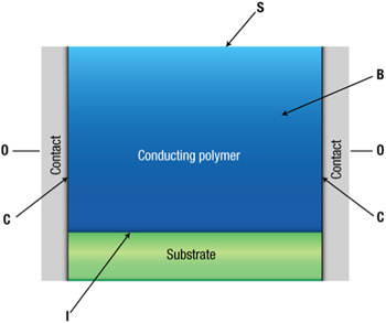
Figure 3. Schematic of a chemiresistor. B: bulk of the conducting polymer. S: surface. I: interface with the insulating substrate. C: interface with the contacts (Reproduced with permission from Nature publishing group.64
Download figure:
Standard image High-resolution imageThese fabrication process, however, still suffer from low device yields, limitation in further miniaturization, scalability, costs, and being limited to gas sensing. Transfer of CPs from the production cell to the microelectrode and minimizing contact resistance between the CPs and the metal pads are still important issues. Although template-free electropolymerization using galvanostatic and voltammetric approaches would help to resolve some of the problems identified above, they still suffer from low device yields and incompatibility in solution,70–73 For instance, the galvanostatic approach require several hours to fabricate the CP nanowires on the microelectrode, and hence not practical for a larger scale production.
A very thin layer of polymer film is preferred for gas sensing application as the sensitivity and response of the resistance changes of conducting polymer films when exposed to gases is increased if the film is thin. To achieve a longer gap length at limited electrode area, interdigitated electrodes (IDEs) are commonly used. The gap between the metal pads in a microfacbricated electrode configuration is usually between 1.5 μm and 100 μm. Deposition through electrochemical methods yield thicker polymer films and therefore in a loss of sensitivity as thicker films block the mass transport of the analyte to the electrode surface.74,75 Pre-treatment of the electrodes with hydrophobic silanes can improve the control and direction of growth of the polymer over the gaps, whereas pretreatment of gold electrodes with thiol modified monomers can improve the contact between the electrode and the polymer film and therefore lower the influence of the contact resistance.
The electrical resistance of a chemiresistive sensor changes when it is exposed to the molecules of analyzing gas. The change in resistance may be positive or negative depends on the nature of sensor materials (n-type or p-type) and the nature of gas molecule (oxidizing or reducing). The CPs can act as electron donor or acceptor as they interact with gaseous species. If a p-type CP donates electrons to the gas its hole conductivity increases. Conversely, when the same CP acts as an electron acceptor its conductivity decreases. CPs can respond to a wide range of polar or nonpolar gases and vapors depending on various interaction mechanisms. For example, the absorption of volatile organic hydrocarbons (VOCs) onto the polymer film causes the conformational changes to the conducting polymer chain either by swelling or alignment of the chains. Swelling of the polymer backbone increase the average electron hoping distance between the chains therefore increases the resistance. However, chain alignment increases chain crystallinity, which decreases the resistance.
The gas molecule X can (i) affect the charge transfer between the polymer and the electrode contact, (ii) can causes oxidation or reduction of the polymer chain thereby changing the density of charge carriers (e.g., ammonia or hydrogen sulfide), (iii) can interact with the mobile charge carriers at the polymer backbone and change the carrier mobility along the chain, (iv) can interact with the counter-ion C- within the polymer film and thus modulate the mobility of the charge carriers along the chain, (v) alter the probability of carrier hopping between chains and thus affect the resistivity of the film, and (vi) can swell the polymer chain thereby modifying the polymer resistivity.
Sensor response and example structure
No matter what recognition mechanism operates, the response is generally rapid and reversible at room temperature, in contrast to metal-oxide sensors that should be operated at elevated temperature. The response function is of the Langmuir type. Accordingly, the resistance increases nonlinearly with the analyte concentration at concentrations below the saturation level. The sensor response can be represented as follows:76
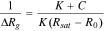
where ΔRg is the change in resistance in the presence of the analyte (ΔRg = Rg – R0), c is the concentration of the analyte, K is the binding constant, R0 is the resistance in the absence of the analyte, and Rsat is the resistance at saturation. Gas permeability through polymer membrane involves three steps. They are (i) adsorption, (ii), diffusion, and (iii) desorption. Once in contact with the polymer, the gas molecules adsorbed to the surface of the polymer are able to diffuse through the polymer membrane. Following diffusion, the gas molecules are transported across the polymer. During the third stage, the gas molecules are secreted from the polymer interface into a lower concentration gradient.
The extent to which a substance can penetrate a polymer depends on sorption (S) and diffusion (D). Sorption is the process by which the gas molecule adsorbs onto the surface of the polymer as a function of its pressure at constant temperature. The process of gas diffusion in polymers can often be described satisfactorily on a macroscopic (continuum) level by suitable solutions of Fick's laws. According to Fick's law, the net rate or flux (J) of gas molecules diffusing through the polymer membrane over time is depends on concentration of the diffusing gas, surface area of the polymer, diffusion coefficient and thickness of the polymer.

where, D is diffusion coefficient (cm/s2), ∂C is change in concentration (g/cm3) of a diffusing gas, and ∂x is change in the distance/thickness of the polymer. Thus, the gas diffusion is proportional to the available surface area while inversely proportional to the thickness of the polymer membrane. A number of factors influences the rate of diffusion. The rates of diffusion are usually higher for atoms diffusing through open crystal structures than for close-packed crystal structures. Deviations from Fickian diffusion arise because of variations in the response of polymer chain segments to a swelling in polymer structure imposed upon the material before and during the sorption-deposition process.
Thus, the gas diffusion transport through complex structured polymeric materials is not accurately described by Fick's law. The diffusion process can be considered in the light of the free volume theory, which considers the creation as well as the size distribution of space required for the motion of the diffusing molecules. The diffusion process thus heavily relies on the ease and degree of packing of the polymer chains. In addition to the crystallinity and of crosslinking as well as additives, such as filler, will affect the gas diffusion. Microscopic theory have been used to model the non-Fickian diffusion process. This model used the Hamiltonian formulation together with Poisson brackets to derive the governing equations for reversible process.70,71 Figure 4 shows the normalized change in resistance as a functional of gold nanoparticles decorated polyaniline (PANI) CP nanowire network towards H2S. The measurements were performed at room temperature with a 0.5 V bias potential and dry air was used as the carrier gas. The nanoparticles functionalized CP nanowire sensor showed an excellent response at concentrations as low as 0.1 ppb. The formation of AuS (reaction of gold nanoparticles with H2S) along with the enhancement of doping level of PANI from the donation of electrons to the protons released in the reaction is assumed to change the resistance of the PANI-gold nanoparticles network.

Figure 4. Response and recovery transients (—) of gold nanoparticles-functionalized PANI nanowire network-based chemiresistive sensor toward 0.1 ppb, 1 ppb, 10 ppb, 100 ppb, 500 ppb, and 1 ppm concentrations of H2S gas (Reproduced with permission from Royal Society of Chemistry.77
Download figure:
Standard image High-resolution imageFuture prospects: problems and possible solutions
Conducting polymer materials exhibit rich collection of morphologies with characteristic porosity that are not only highly dependent on the monomer and synthesis route but are also shown to significantly affect their sensitivity and response times in gas sensing applications. Long-term instability is a main drawback of the sensors based on conducting polymers, as they are thermally unstable, so it is often impossible to use them at temperatures at which gas-solid interactions proceed rapidly and reversibly. Sensors based on conducting polymers are usually sensitive to water, so humidity must be considered when detecting other gases in air. Nearly all the conducting polymers are sensitive to redox-active gases, such as NH3 and NO2, and for organic vapors. So the interactions between analyte and conducting polymer need further investigations.
Second, relatively lower stability of conducting polymers is the main drawback of these sensors. Swelling effect often occurs in conducting polymer layers, which can cause electrical resistance change in chemiresistor. Both chemical and physical properties of conducting polymer strongly depend on the ambient conditions, such as temperature and humidity. Thus, how to prolong the lifetime of sensors is the critical obstacle in application of conducting polymers, and the main challenge to the researchers in the field. Third, a great deal of effort has been devoted to adjusting the side chain structures of conducting polymers, to promote sensing performance. However, most of these attempts are concentrated on conjugating commonly available side chains with the CPs. Molecular modelling studies correlating side chain structure with binding activity has not been widely considered when developing new sensing materials. Inducing new functional side chains on conducting polymer backbone is expected to obtain new class of materials with special sensing capability.
Carbon based
Carbon nanotube based
Core technology.—Carbon nanotubes (CNTs), collectively encompassing both multi-walled carbon nanotubes (MWCNTs) and single-walled carbon nanotubes (SWCNTs) can provide solutions to detection of toxic gases, VOCs, and hydrocarbon emissions in environmental, manufacturing, and human health monitoring. Gas sensors dedicated to toxic gases typically use semiconducting metal oxides (e.g. SnO2) or conducting polymers. As a general comparison, conventional solid-state sensors for NO2 and NH3 operate at temperatures over 423 °C, while conducting polymers provide only limited sensitivity. By comparison, SWCNTs and MWCNTs sensors can operate at room temperature with response times of 10's of seconds with ppm detection levels. As sensing materials, SWCNTs and MWCNTs behave as p-type semiconductors. When electron-withdrawing molecules (e.g. NO2, O2) or electron-donating molecules (e.g. NH3) interact with the p-type semiconducting CNTs, they will increase/decrease the main charge carrier (holes) density in the CNTs. In fact, experiments have shown that NH3 donates about 0.04 electron per molecule to SWNTs,78 while NO2 withdraws approximately 0.1 electron per molecule with binding energy of 0.8 eV.79 In turn, by measuring the change in the conductance of nanotubes, gases are detected and/or monitored. This behavior forms the basis for applications of CNTs as electrical chemical gas sensors. This mechanistic picture is supported by many theoretical papers and first-principle calculations using density functional theory.
Detection however relies upon adsorption, meaning that the adsorption energy (or affinity) must be comparable or greater than kT for sensing to occur, k being Boltzmann's constant, and T absolute temperature in Kelvin. Gas sensors based on pristine CNTs have certain limitations, such as low sensitivity to some adsorbates for this reason. Defect free MWCNTs have a surface equivalent to graphite—possessing little adsorption affinity to most gases. Alternatively, if the adsorption energy is too high the sensor will have long recovery times or potentially suffer irreversibility. As an illustration, chemiresistors made with defective CNTs exhibit a greater sensitivity toward NO2 compared to defect-free sensors.80 This observation is consistent with theoretical calculations indicating that the defect sites on the CNTs result in a strong chemisorption of NO2 and a large charge transfer interaction. In a similar way, MWCNTs chemically oxidized and full of defects can detect a few ppm of NO2 and NH3 while there is almost no response in pristine (not acid treated) nanotubes.81 This dependence upon defects as adsorption sites creates both problems and opportunities.
Sensor design and transduction/sensing (detection) mechanism.—CNTs act as both sensing materials and as transducers. Two different configurations, a chemical resistor (chemiresistor) and back-gated chemical field effect transistor (ChemFET) have been utilized. Figure 5 presents schematics for each. In the chemiresistor configuration, a single CNT or network of CNTs bridges the positive and negative electrodes through which current is passing. As earlier described, the binding of analytes on the CNT surface results in charge transfer between the adsorbate and the surface of the CNT, altering its electrical resistance. The back-gated ChemFET configuration is similar to the chemiresistor except that the conductance of the CNT between the two electrodes, (now referred to as source and drain) is modulated by a third electrode, (gate electrode), capacitively coupled through a thin dielectric layer, usually a SiO2 layer. In general, ChemFETs tend to be more sensitive than chemiresistors because of the ability to tune the conductance of CNTs by controlling the gate voltage. This makes ChemFETs ideal candidates for electrically based sensing, although the ChemFETs require slightly more complex ancillary electronics than do chemiresistors. Both configurations generally use interdigitated electrodes or similarly interlaced electrodes to maximize CNT bridging material. CNTs may be grown directly on these electrodes via controlled CVD, or drop-cast from a suspension or solution. Screen-printing can also be employed. Dielectrophoresis has often been used in conjunction with drop-casting to achieve (partial) alignment of the bridging CNTs (SWNT or MWNT). Other deposition methods include electrophoretic deposition, spin coating, inkjet printing, etc. Other types of CNT sensors are based on SAW,82 capacitive83 and gas ionization84 as the operative signal transduction technology, in contrast to voltage-current characteristics as in chemiresistors or ChemFETs.
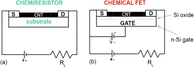
Figure 5. Electrical schematics of a chemiresistor (a) and ChemFET platform (b).
Download figure:
Standard image High-resolution imageSensor response and example structure.—To give a sense of capabilities based on CNTs, Table I provides a snapshot of selected results: gases, responses and detection limits, for varied CNT based chemiresistors. Figure 6 shows the response curves for MWCNTs, pristine and decorated with Au or Pt nanoparticles. The opposing conductivity changes are clear—in response to electron donation or withdrawal by NH3 or NO2 respectively. The gains in response by the catalytic action of the noble metals is significant.
Table I. Gases, responses and detection limits for varied CNT based chemiresistors.
| CNT Form | Gas Detected | Response time | Detection limit (ppm) | Reversible | References |
|---|---|---|---|---|---|
| SWNTs | NO2 | Few minutes | 44 ppb | Long, accelerated by UV irradiation | 85 |
| Nitrotoluene | 262 ppb | ||||
| SWNTs | O3 | <600 s | 6 ppb | Yes | 86 |
| MWNTs | NH3 | <600 s | 5–10 ppb | Yes | 87 |
| MWNTs | NH3 | ∼100 s | 10 ppm | Yes | 88 |
| Pd/SWNTs | H2 | <600 s | 10 ppm | Yes | 89 |
| MWNT-SnO2(Sb) | HCOH, NH3, C6H6, C7H8 | <10 s | 500 ppm exposure, LOD not specified | Yes | 90 |
| Ag-MWNT (plasma treated)-SnO2 | NO2 | ∼2 min | <100 ppb (at 150 °C) | Yes | 91 |
| CO | <10 ppm (at 150 °C) |
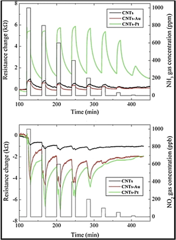
Figure 6. Time response of the electrical resistance change for a chemiresistor based on (black) pristine MWNT films and (green) Pt- and (red) Au-modified MWNT films toward (top) NH3 and (bottom) NO2 gases at working temperature of 150 °C.92
Download figure:
Standard image High-resolution imageWhile these results are impressive for sensitivity at room temperature (except where noted), there are both unknowns and caveats. Both experimental and theoretical studies show that the sensitivity of CNT sensors can be improved by doping the CNTs or by introducing defect sites along the sidewall of the CNTs during the purification (oxidation) process. Comparison between defective and defect-free CNTs in a chemiresistor configuration revealed that defective CNTs exhibited a greater sensitivity toward NO2 compared to defect-free sensors.87 This observation was consistent with theoretical calculations indicating that the defect sites on the CNTs resulted in a strong chemisorption of NO2 and a large charge transfer interaction, while the defect-free CNTs had a very weak interaction and negligible charge transfer. Terminology usage in the literature is inconsistent, to some, "pristine" CNTs may mean non-functionalized, or perhaps "as-prepared," or even after purification by acid etching or oxidation. Pristine does not necessarily imply without defects, and all CVD produced CNTs possess such. Without detailed surface chemistry characterization, sensor response can vary widely. The bandwidth of variation as dependent upon "defects" has not been mapped, and such a study would surely be a landmark reference, if done properly. Additionally, the vast majority of tests for response are conducted under a controlled atmosphere consisting solely of the target analyte in an inert gas background. As illustration, the resistance of MWCNTs has been observed to increase upon exposure to humid air. This effect was explained by the formation of hydrogen bonds from polar water molecules with oxygen-containing defects on the MWNTs.93 This reduced the electron-withdrawing power of the oxygen-containing defect groups, thus increasing the density of holes in the MWNTs thereby increasing the electrical resistance. Similar enhancement of sensing was observed for the sensing of CO.
Functionalized CNT sensors often offer a higher sensitivity and a better selectivity compared to pristine CNT sensors. Agents can include conducting polymers or metal nanoparticles. Although CNTs have proven to be a good gas sensing material, pure CNTs show no response to H2 due to the weak binding energy.94 However, when functionalized with Pt or Pd, which act as a catalyst for the adsorption of H2, CNTs can be very sensitive to hydrogen. The presence of different metallic particles functionalizing the CNT walls make the CNTs sensitive to several gases at room temperature. Deposited at the surface of SWNTs by electron-beam evaporation, adsorbed H2 molecules are dissociated as hydrogen atoms, which dissolve into Pd with a high solubility, leading to a decrease in the work function of Pd. This causes electron transfer from Pd to SWNT and reduces the hole carriers in the p-type SWNT, and hence causes a decrease in conductance. The process is reversible as dissolved atomic hydrogen in Pd can combine with O2 in air to form OH, which will combine with atomic hydrogen to form water that can leave the Pd–SWNT system, thus recovering the sensor's initial conductance. This quick and easy recoverability make the Pd-coated nanotubes suitable for practical applications in room temperature hydrogen sensing while consuming only ∼0.25 mW power.
Similarly, the sensitivity of Pt- and Au-functionalized MWNTs towards NH3 and NO2 improved by one order of magnitude.92 More elaborate systems include Au/CNT/SnO2 or Sb/CNT/SnO2, as examples (see Table I), for the identification of CO, NH3, formaldehyde, toluene, NO2, benzene and O2. With the frame of reference being the metal oxide material, these hybrid materials improve detection by a factor of 2–5 relative to the pure metal oxide while also enabling lower temperature operation. The observed response is attributed to a sequence of charge transfer interactions between adsorbate-metal oxide and CNT. Cogent descriptions are lacking, as are guiding theoretical calculations.
Future prospects: problems and possibilities.—Criteria for gas sensing include high sensitivity and selectivity, fast response and recovery times, and stability. For detection of reactive gases, e.g. hydrocarbons, or toxic gases, e.g., NO2, NH3, semiconducting metal oxide sensors must operate at high temperatures (up to 600 °C) for high sensitivity. In contrast, SWNT chemical sensors show strong responses even at room temperature. However, the disadvantage with using a SWNT chemical sensor is the long recovery time needed to release the analyte at room temperature. This slow recovery remains a major drawback for nanotubes-based chemical sensors.95
To accelerate the recovery process for restoring the initial conductance of CNT sensors, an external energy source may be implemented to rapidly desorb strongly adsorbed analytes by lowering the adsorption energy barrier. This can be achieved by local heating of the nanotubes to high temperatures (∼200 °C), or using photo-induced desorption, such as ultraviolet light illumination. It has been demonstrated by several researchers that UV light (250 nm) at low photon flux causes rapid desorption of adsorbed species from the SWNTs at room temperature. ChemFETs have the advantage of reversibility by back gating, applicable for weakly-bound adsorbates.
A potential drawback of using non-functionalized CNTs as sensing elements is the lack of specificity to different gaseous analytes and the low sensitivity towards analytes that have no affinity to CNTs. These shortcomings can be partially circumvented by functionalizing the CNTs with analyte specific entities. Two main approaches for the surface functionalization of CNTs: covalent functionalization and non-covalent functionalization. However, functionalization can also affect the sensor sensitivity and response time.
A fundamental issue are defects. By most synthesis methods and certainly by all purification processes, CNTs possess defects, uncontrolled in number and unknown in type. Dangling bonds, vacancies, and of course oxygen groups are considered defects, enabling strong physisorption if not chemisorption. Some studies have sought to exploit this by plasma-treating the CNTs,93 applying acid washing,94 or by doping heteroatoms such as boron or nitrogen.96 The oxidation methods lead to a variety of defects and oxygen groups while doping at least maintains site consistency. By whatever approach, consistency of material and response will necessarily precede rational design of analyte specific sensors and monitoring networks.
Graphene based
Core technology.—Gas sensors can detect combustible, explosive and toxic gases, and have been widely used in safety monitoring and process control in residential buildings, industries and mines. Metal oxides such as zinc oxide (ZnO), stannous oxide (SnO2), tungsten oxide (WO3), cuprous oxide (Cu2O), etc. have widely been explored for sensing applications, mainly due to their large specific surface area, excellent mechanical flexibility, and good chemical stability.97 However, these sensors hold an obvious disadvantage of high operating temperature, resulting in high power consumption, which in turn adversely affects the integration and long-term stability. Since graphene is a two-dimensional material, every atom of graphene may be considered a surface atom and as a result, every atom site may be involved in the gas interactions. The  and
and  * orbitals, can behave like valence band and conduction band, respectively. But, the problem with intrinsic graphene is that it has no dangling bonds on its surface (required for gas/vapor adsorption) and therefore to enhance chemisorption, it generally needs to be functionalized with polymers, metals or other modifiers. The thin coating of functionalizing materials behaves as trapping centers for target species and the adsorption introduces a local change in electrical resistance of graphene sensors.
Though a similar approach has been already well established in chemical sensor research, the unique advantage in case of graphene is its extremely high electrical conductivity (even when few carriers are present) along with low noise which makes this change in resistance detectable even to sub ppm level.98 The different synthesis procedures for graphene have recently been critically and elaborately reviewed by Seal et al.99 Experimentally, exfoliation of graphite has been investigated and realized by using various techniques, including chemical or solution, mechanical, and thermal methods. Graphite is stacked layers of many graphene sheets, bonded together by weak Van-der-Waals forces. Synthesis of graphene sheets via chemical routes poses potential challenges in sensor development based on these materials. Efforts are required for achieving an understanding of the intercalation, oxidation, exfoliation, reduction, functionalization, and dispersion processes and for developing new starting materials and reaction routes. Figure 7 illustrates the different chemical forms of so-called "pristine" graphene (PG), graphene oxide (GO) and reduced graphene oxide (RGO). Notably despite the specific nomenclature, it is important to understand that there is no singular composition, shape or size for any given form. Each form has a continuum of variations in size and composition, details dependent upon preparation process.
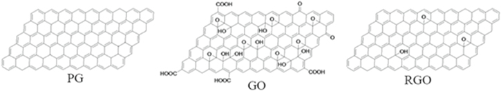
Figure 7. Illustration of the different chemical forms of pristine graphene, (PG), graphene oxide (GO), and reduced graphene oxide (RGO).
Download figure:
Standard image High-resolution imageBriefly, the micromechanical (scotch tape) method produces high quality material; it is a simple and low-cost method, but offers poor control. It produces graphene sheets tens of microns in size, and is not suitable for mass production. Chemical vapor deposition (CVD) produces high quality material (single layer to a few layers), and offers large scale production. The graphene can be transferred relatively easily to any substrate with good control. This method is relatively costly and hazardous (due to use of chemicals and high temperature). Importantly it is very inert due to absence of functional groups. Epitaxial growth (CVD on epitaxially matched surfaces) produces high quality graphene with good control. By this method, it is difficult to control surface morphology. It is a high temperature process, the role of the interface is not well understood, and in general, this method is not for mass production. Chemical exfoliation (reduction of GO) produces relatively cheap material, and is suitable for large scale synthesis. There is no need of substrate. The presence of functional groups makes these materials reactive. The process offers at best moderate control of the oxygenation level. It requires several process steps and requires the use of hazardous chemicals. The resulting GO is characterized by the presence of residual oxygen and moisture; it has very poor electrical quality and contains many defects and functional groups. Yet other methods include thermal exfoliation, i.e. unzipping CNTs. The material has mixed quality, is high cost and this process is not suitable for mass production. In general, a cost-effective method to produce graphene-based devices in large quantities is to first produce GO (chemically modified graphene) by the oxidative exfoliation of graphite and to subsequently reduce it to graphene by chemical or thermal means using reducing agents or high temperature annealing to form reduced graphene oxide (RGO). The point is that there is no one process, nor form of graphene, graphene oxide or reduced graphene oxide. The plethora of pathways and products has created a diversity of opportunity as briefly highlighted following. Contrarily, this same diversity had led to high variability, inconsistencies, and poor understanding of the underlying physics and chemistry, giving rise to the observed response.
The "core technology" is that the adsorption of gas molecules on graphene's surface leads to changes in its electrical conductivity that can be attributed to the change in the local carrier concentration induced by the surface adsorbates which act as electron donors or acceptors.100 A typical p-type response is observed by testing in both reducing and oxidizing environments. Gas-induced changes in resistivity have different magnitudes for different gases, and the sign of the change indicated whether the gas was an electron acceptor (e.g., NO2, H2O) or an electron donor (e.g., NH3, CO, ethanol). In general, the interaction between graphene sheets and adsorbates can vary from weak van der Waals to strong covalent bonding. All these interactions change the electronic structure of graphene, which can be readily monitored by convenient electronic methods. Leenaerts et al.101 studied the interactions between PG and different gas molecules such as H2O, NH3, CO, NO2 and NO using first-principles simulations based on density functional theory (DFT) calculations. Their results showed that CO, NH3, NO2, H2O and NO are physically adsorbed on PG. Moreover, the charge transfer analysis indicated that NO2 and H2O serve as acceptors whereas CO and NH3 serve as donors in agreement with the experimental findings of Schedin et al.100
The problem with intrinsic graphene is that it has no dangling bonds on its surface (which is can be desirable for gas/vapor adsorption) to enhance the chemisorption of target molecules on graphene surface. Therefore, graphene needs to be functionalized with polymers, metals, or other suitable modifiers. The thin coating of functionalizing materials enhances the adsorption of target species that causes a local change in electrical resistance. Doping or surface modifications especially by catalytic noble metal ions is well established in chemical sensor research. The special advantage with graphene is its extremely high electrical conductivity (even in presence of few carriers) and low noise that make the detectable change in resistance even down to sub-ppm and ppb level of the target species.98 Yet better chemical affinity and selectivity102 can be achieved by functionalization of graphene or reduced graphene oxide.102,103
Sensor design and detection mechanism.—The transduction of the sensing signal can exploit both the electronic and mechanical properties of graphene. Notably graphene and its oxidized form can be produced more economically than the carbon nanotubes, presently popular for sensing platforms. While many platforms exist for graphene-based sensors, in chemiresistors and ChemFET configurations the graphene sheets bridge opposing electrodes. Figure 8 schematically shows graphene oxide as bridging opposing electrodes in a chemiresistor platform. These may be in the form of simple pads, a variety of interdigitated patterns. These in turn may be fabricated by photolithography methods atop non-conductive oxides, oxide layers atop a third electrode as in ChemFETs or upon micro-hotplates. Either electrons or holes can serve as the major charge carriers in graphene FETs depending on the value of gate potential (Vg). The graphene FET operated at high positive Vg in n-mode exhibited superior performance for the detection of NH3 compared with that in p-mode. This is mainly because a positive Vg lowers the work function of graphene, decreasing the electron transfer barrier between graphene and NH3 and also decreasing the barrier of NH3 desorption. Yet additional platforms include SAW or QCM as the signal transduction mechanism rather than change in conductivity.

Figure 8. Illustration of graphene oxide in a chemiresistor sensor.
Download figure:
Standard image High-resolution imageLike the sensing principle of usual semiconducting metal oxides, the conductivity of graphene also varies upon exposure to the target species (gas/vapor). The sensing species act as temporary dopants to the graphene layer and change its localized electronic concentration contributing thereby either electrons (like the case with NH3 and CO) or holes (the case with H2O and NO2), resulting in resistance change. Thin layers of graphene can be fabricated from their suspension by drop casting, spin coating, spray coating or dip coating technique.104–106
Most graphene-based gas/vapor sensors reported have operated in the resistive mode107 where the resistance change (i.e. current voltage characteristics) upon exposure to the interacting gas/vapor is directly measured. This design is simple, offering ease of fabrication and direct measurement. Graphene based sensors may use epitaxially grown graphene on substrate/sensing platform, or use varied forms of graphene, reduced graphene oxide or varied forms of functionalized graphene (or RGO) deposited on the platform as the sensing layer. This leads to simple and reproducible device fabrication.104,108
Sensor response and example structure.—Pristine graphene (Gas adsorption on pristine graphene).—Pristine graphene (PG) is considered as a pure and defect free form of graphene, which is normally derived from graphite exfoliation or CVD growth methods. Electron acceptors such as NO2, H2O and electron donors such as CO, NH3 are differentiated by observing their effects on resistivity i.e. increase or decrease respectively. On the other hand, Dan et al.109 concluded that the observed high sensitivity of PG towards various gases is attributed to the chemical doping of graphene by the contamination from device fabrication and proved that the intrinsic sensitivity of PG is low even in the presence of strong analytes. Regardless, for gases with strong interactions with graphene, e.g. NO2 and NH3, high temperature annealing in vacuum is required for desorption.
Most of the CVD-graphene-based gas sensors described above have poor reversibility, similar to the devices based on carbon nanotubes.110 Thermal energy is frequently insufficient to overcome the activation energy for desorption. Supplementary heat for thermal desorption, light for photo-desorption, or reverse bias in the case of a ChemFET is necessary for practical recovery times. For contrast, ozone-treated graphene demonstrated significant enhancement on the sensing performance compared with the pristine graphene. The percentage response of this sensor to 200 ppm NO2 was 2 times stronger, and the response time was eightfold faster than for a pristine graphene sensor. Moreover, a low limit of detection (LOD) of 1.3 ppb was achieved. These performance improvements were attributed to the favorable gas adsorption sites provided by the oxygen containing groups.
Defective graphene (Gas adsorption on modified graphene).—Theoretical studies have also proved that introduction of defects and dopants on graphene drastically improved the sensitivity of graphene-based gas sensors by stronger adsorption of gas molecules on defective and doped graphene as compared to PG.111,112 Zhang et al. observed strong interactions between small gas molecules such as NO2, CO, NO, NH3 and on modified graphene, (doped with boron, nitrogen or by introduction of defectives, BG, NG and DG, respectively) than with PG by performing DFT calculations. The adsorption energies of gas molecules on modified graphene are higher than that on PG and the charge transfer between gas molecules and modified graphenes are larger. Confirmed by experiments, graphene doped with B-, N- or Si-dopants has shown strong binding with most common gases such as H2, H2O, O2, CO2, CO, NO2, NO, SO2, NH3 and N2.113 Yet to further gain, graphene modified with defects and transition metal dopants such as Ca, Co, Fe exhibited much higher affinity to H2S compared to PG, BG and NG.114
Graphene oxide (GO) (Gas adsorption on GO).—Chemical oxidation of graphite and simultaneous reduction of resulting graphite oxide is one popular approach used for graphene synthesis. Graphite oxide has a layered structure analogous to graphite, but is heavily decorated with oxygen-containing groups such as hydroxyls, epoxies, carboxyl and lactones. These functional groups not only expand the interlayer spacing but also make the atomic-thick layers more hydrophilic and enabling these oxidized layers to exfoliate in water under moderate ultra-sonication or stirring. The single or fewer layers of exfoliated graphite oxide is often termed as GO.115 Owing to its oxygen rich functional groups, the GO is a potentially promising candidate for gas sensing. Clear disadvantages are its low conductivity (dependent on the degree of oxidation) and strong interaction between reactive adsorbates and the oxygen groups—limiting reversibility and repetitive use.
Using first-principles study, Peng et al.112 find that GO is better than graphene for the detection of ammonia, since the active defect sites of GO such as the epoxy and hydroxyl groups promote the interactions between the ammonia molecules and GO. Similarly, first-principles calculations demonstrate that hydroxyl, carbonyl groups on the GO surface result in large binding energies and enhanced charge transfer from nitrogen oxides NOx (x = 1, 2, 3) to GO, leading to chemisorption of gas molecules on GO.116 Even though GO is electrically insulating due to numerous oxygen functional groups, the conductivity can be restored to several orders of magnitude by the removal of oxygen groups using chemical or thermal reduction which does not produce PG due to the residual oxygen groups that remain on the RGO surface even after GO reduction. However, the capacity of gas adsorption will decrease if all the oxygen-containing functional groups are reduced because they are active sites for gas adsorption. There is therefore a balance between the adsorption capacity for gases and the electronic conductivity of RGO during the GO-reduction process.117 Consequently, RGO possesses chemically reactive oxygen "defect sites" and greater conductivity than GO, that makes it highly promising for gas sensing.118 DFT calculations and in situ infrared (IR) spectroscopy experiments on NH3 adsorption on RGO119 revealed that the interactions between NH3 and RGO yields different surface species: physisorbed NH3, a wide variety of chemisorbed fragments (e.g. NH2, OH and CH), likely due to the dissociation of NH3 at the carbon vacancies and the epoxide groups—all leading to resistance change.
For gas sensing, RGO has proved advantageous over PG considering the low production costs, tuning of structure and properties such as conductivity, dispersal in water, and possibility of further modification by functionalization. Hence, RGO based sensors have been studied in detection of various gaseous species.108,117,120,121 Illustrating the advantage of RGO, non-reduced, as prepared GO sheets showed no response to NO2 or NH3, indicating negligible change in the electrical transport property of the non-reduced GO. The thermally-reduced GO showed p-type semiconducting behavior in ambient conditions and was responsive to low-concentration NO2 and NH3 gases diluted in air at room temperature. (GO annealed at 300 °C showed high sensitivity (∼1.56 to 100 ppm NO2) and fast response, compared to GO annealed at 200 °C with sensitivity of ∼1.41).100 The good response of the partially reduced GO sensor is attributed to the recovery of carbon atoms, vacancies, or small holes created during the thermal treatment that act as active sites for gas adsorption. As suggested by Leenaerts et al.101 on the basis of first principle study, NO2 is a strong oxidizer with electron-withdrawing power; therefore, electron transfer from reduced GO to adsorbed NO2 leads to an enriched hole concentration and enhanced electrical conduction in the reduced GO sheet.117
However, molecular adsorption of gases onto RGO containing oxygen functional groups is problematic. Acting as higher-energy binding sites, desorption is non-recoverable without external assistance, due to the strong binding of gases on these sites. This degrades the sensing performance because the change in conductance during the sensing cycle does not return back to its base value even after removing the target gas supply and this change passes on to the next sensing cycle. Moreover, given the variability in RGO production, consistency is problematic between different batches.
Hybrid forms—graphene with functionalization/doping.—Usually sensing applications based on graphene require chemical modification to control the physiochemical properties, and at very least impart greater sensitivity by increasing adsorption affinity. Chemical modifications include introduction of defects and dopants (e.g. sulfur, boron, silicon)111,122,123 coating with metal,124,125 and metal oxide nanoparticles,126,127 and polymers.128 Notably the metal and metal oxide nanoparticles activate adsorption, i.e. they promote chemisorption—usually resulting in a larger change in conductance.
As an example, Pt decorated graphene exhibited a 2-fold increase in sensitivity of Pt decorated MWNT but with a comparable response time at room temperature, whereas Pd-decorated graphene sensors exhibit significant resistance changes, while no detectable change was observed in the case of PG.124 The reported increase in resistance is due to the lower work function of Pd hydride, enabling transfer of more electrons from Pd NPs to graphene (thereby cancelling the p-conductivity of native graphene). A sensing response of 33% to 1000 ppm H2 and a detection limit of 20 ppm H2 at ambient temperature (22 °C) were shown by a graphene sensor with a 3 nm thick Pd coating, thermally evaporated.39 The sensing performance of RGO to NH3 was found to be greatly improved by the decoration with Ag NPs.129 The sensitivity was about twice than that of multi-walled CNT (MWCNT)/Ag hybrids, but comparable response and recovery times of 6 and 10 s respectively. As with semiconducting metal oxides, the noble metal aids H2 dissociation, leading to subsequent diffusion of H atom through the metal to graphene surface, which eventually resulted in higher response magnitude. As further illustration, Pd decorated graphene was found to be capable of detecting hydrogen at levels from 0.5 to 1% in synthetic air. Pure graphene is poorly sensitive to hydrogen, but incorporation of Pd increases its sensitivity by more than an order of magnitude.
Other synergies exist in such nanoparticle-graphene hybrid systems. The graphene substrate can increase the conductivity relative to the pure metal oxide while the metal oxide or metal nanoparticles can prevent re-aggregation of the graphene. When GO is hybridized with metal oxides, it usually needs to be reduced by thermal-reduction or chemical-reduction methods to improve the conductivity. The sensing mechanism(s) are not entirely clear, however. The metal oxides possess depletion layers. There are also p-n junctions between p-type graphene and n-type metal oxides, which modulate the space-charged layers at the interfaces between graphene and metal oxides.
Graphene oxide decorated with ZnO for efficient detection of CO, NH3, and NO with appreciable selectivity towards electron donor gases like CO and NH3.127 Two different depletion layers co-exist, one on ZnO surface and the other at the interface of graphene oxide and ZnO. Operationally both contribute. Notably the ZnO–GO composite sensor is more selective to reducing gases and shows a poor response to oxidizing gases (here NO).130 This can be understood by the additional electron withdrawal from the metal oxide by an oxidizing gas contributes relatively little to the existing depletion layers at the metal oxide and metal oxide-graphene interface. One principle advantage of such composite sensors is that thermal activation of ZnO nanoparticles is eliminated, leading to room temperature sensing.
In a SnO2-RGO hybrid sensor the sensitivity to NO2 increased (from 2.16 to 2.87), while the sensor sensitivity to NH3 decreased substantially (from 1.46 to 1.12).126 In open air, the first depletion layer is due to the adsorption of ionized oxygen (O2−) at the surface of the SnO2 nanoparticles on SnO2–RGO heterojunction. Target gas molecules (e.g., NO2) directly adsorb on the surface of the SnO2 nanoparticles and modify the depth of the first depletion layer, which in turn alters the depletion layer at the SnO2–RGO interface. (At the interface between the SnO2 (n-type) and the RGO (p-type), due to formation of p–n junction and the depletion zone, more electrons are attracted from the RGO toward SnO2 in NO2.131 Effectively the Fermi level of the RGO shifts towards the valence band, enhancing the RGO conductivity. In the case of NH3, because of the p–n junction and hole depletion zone, fewer electrons are (comparatively) injected into the RGO resulting in a decrease of RGO conductivity compared to that of the pure RGO. Nevertheless, the mechanism of the gas-sensing of SnO2–RGO sensor needs further investigation. For example, the attachment of SnO2 nanoparticles onto RGO leads to more active sites (such as vacancies, defects, oxygen functional groups as well as sp2-bonded carbon) for the adsorption of NO2 molecules, and thus, a higher sensitivity than pure RGO.
Additional data obtained with the pure SnO2 and RGO sensors indicated that SnO2 behaves as a n-type semiconductor whereas reduced graphene oxide as a p-type semiconductor.132 This leads to the formation of an n–p heterojunction at the n-SnO2/p-RGO interface of the hybrid structures. By increasing the density of SnO2 particles on the graphene sheets, the "shortcuts" between RGO and RGO are reduced so the RGO–SnO2–SnO2–RGO junctions become more effective. A similar mechanism has been previously demonstrated to be responsible for the enhanced sensor response to NO2 on CNT–SnO2 hetero-structures.133 A comparative advantage is that the RGO sheets can increase due to an effective dispersion of the metal oxide phase—on the RGO sheets.
Interestingly, graphene based ternary composites have also been analyzed for understanding their gas sensing properties. In this direction, Wang et al.134 prepared a CuO–ZnO/RGO composite. The successful anchoring of large number of nanoscale p–n junctions between CuO and ZnO NPs onto RGO sheets promotes the sensing behavior towards acetone. Other modifications include functionalization of RGO with quantum dots,135 nanowires136 and CNTs.137
Future prospects: problems and possibilities.—Graphene based sensors offer opportunity. Pristine graphene is relatively insensitive to all but strong oxidizing and reducing gases, and then with poor recoverability without assistance. Low quality and defective graphene may be more useful for gas sensor applications because defects and oxygen groups can serve as active sites for strong physisorption or chemical adsorption. Both have drawbacks for sensor temporal dynamics. Physically engineering defects by tailoring the size of graphene such as ribbons is an intensive effort and not well suited to mass reproducibility. Consistency of the material, reproducibility of response, and achieving selectivity are key challenges that have not been met. The dependence of sensor response to the level of oxygen atom content, distribution of oxygen functional groups by type (e.g. phenolic, carbonyl, carboxylic and epoxide), their spatial distribution across the graphite sheet has yet to be systematically studied. Further insights on theoretical studies are also needed to better understand the interaction mechanism between various gases and graphene-based functional nano-hybrids consisting of metals or metal oxide nanoparticles.
For real life applications, one should note that the performance of these sensors might strongly depend on the relative humidity of the environment. Depending on the level of humidity which can range up to thousands of ppm in the real-world environment—in which the sensors are to be operated, their ability of detection of gases can be completely screened.138 GO films have also been effectively used in humidity sensing applications. Bi et al.139 have used GO to fabricate a microscale capacitive humidity sensor. It was reported that compared with conventional capacitive humidity sensors, the GO based humidity sensor has a sensitivity of up to 37,800%, which is more than 10 times higher than that of the best one among conventional sensors at 15%–95% relative humidity. The excellent humidity sensing ability of GO is attributed to its hydrophilicity. While this is a stellar result, it underscores the problem that GO based sensors would face in real environments for other target gases with background humidity. Hence, the success of graphene-based sensors largely depend on their sensitivity to humidity and indeed graphene based humidity sensors are well reported. Despite this, most reports on graphene based toxic gas sensors are based on measurements in dry air or in vacuum. Consequently, it is not possible presently to compare the influence of humidity on different graphene based sensors. Another area where graphene–metal oxide based sensors need attention is to explore their ability to sense nonpolar and large molecules. Until now most of the published work on graphene-based sensors have focused on detection of polar molecules such as NO, NO2, H2S, NH3, etc.
Resonators and mechanical chemical sensors
Core technology
Resonating devices are in widespread use as timekeeping components and frequency-selective filters in communication systems, consumer electronics, and computers. Resonators with stable and precise frequencies are important in these applications, and therefore controlling the operating environment is critical. However, for sensing, several different requirements are necessary. The influence of small changes in mass, stress or temperature form the basis of sensitive detection with resonators for chemical sensing. For example, chemical or biological targets, which selectively bind to the resonator surface, produce a shift in resonant frequency, damping or changing the wave velocity that facilitates detection. Figure 9a illustrates how a change in mass or layer thickness in a thickness-mode resonator produces a decrease in resonant frequency and Fig. 9b shows a phase shift can be induced in the case of a surface acoustic wave resonator.
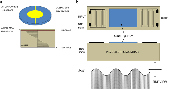
Figure 9. (a) Diagram of QCM resonator based upon AT-cut quartz disk where a change in mass/thickness of the sensing layer lowers resonance. (b) Diagram of SAW sensor using two sets of interdigitated electrodes with sensing film between them. The side view illustrates the surface wave motion.
Download figure:
Standard image High-resolution imageFigure 9a shows the basic operation and function of a quartz crystal microbalance (QCM) resonator. In this device, a bulk vibration often known as Thickness Sheer Mode (TSM) is generated in the crystal. The electric field at the surface produced by electrodes produces a tangential deformation at top and bottom surface of the crystal, such that they move in parallel, but in opposite directions. The wavelength of the vibration is given by the boundary conditions on the plate: nλ = 2d, where d is the thickness of the resonator and n is an integer number.
However, the shift due to added mass can be calculated using Sauerbrey's equation.140

where Δf is the change in frequency produced by the adsorbed mass, Δm, f0 is resonant frequency, ρ is density and μ is the shear modulus. A is a constant based upon the mechanical and electrical characteristics of the QCM. The change in frequency with mass is larger at higher frequency of operation (Eq. 6). However, limit of detection is determined by signal-to-noise ratio, so that the increased noise at higher frequency results in an approximate linear decrease in LOD with frequency. Because of the thickness of the QCM is limited by the fabrication technology, those frequencies above 100 MHz are difficult to reach. Higher frequency QCMs have been micromachined in quartz substrates by Tadigadapa et al.141
Surface Acoustic Wave (SAW) devices can also be used for sensing. An interdigitated electrode (IDE) array generates a surface acoustic wave, also known as a Rayleigh wave which propagates along the surface. These waves have a transverse motion and penetrate a depth of at least one wavelength into the substrate. The designed wavelength sets the IDE's spacing, which is typically less than 0.002 mm, and therefore defined by photolithography. The electrodes are generally an inert metal, such as gold to provide high conductivity and corrosion resistance during sensing. A second set of IDE picks up the acoustic wave and the change in amplitude and phase of the signal are measured, typically with a feedback loop using an amplifier. Excellent reviews of SAW devices have been published by Grate,142,143 and Ballantine et al.144
For bio-sensing, the two sets of interdigitated electrodes are separated by a gap in which there is the antibody layer for protein binding. For gas sensing, a vapor is adsorbed onto the sensing polymer layer and the physical changes provide a response based upon mass loading and changes in the electrical conductivity of the film. Surface acoustic wave devices can be differentiated from bulk acoustic wave device in the local confinement of the acoustic energy near the surface of the structure.
Other types of acoustic wave sensors include Acoustic Plate Mode (APM) sensors and Flexural Plate Wave (FPW) sensors. An APM has a similar geometry to SAW except this type of a device is much thinner, actually just a couple of wavelengths thick so a SAW and bulk sheer horizontal mode move through the substrate. In FPW devices, a thin plate is driven into oscillation using a piezoelectric material, a magnetic field or electrostatic actuation to generate displacement in the thin plate with conductive strips (see Fig. 10). The FPW devices have the advantage of lower oscillating frequency and ability to isolate the IDE from the measurement medium. Further details of these sensors can be found in application to biosensing.145
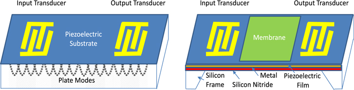
Figure 10. Principle of sensing for an APM (left) and FPW (right) type sensors.
Download figure:
Standard image High-resolution imageIn a bulk acoustic resonator, the standing acoustic wave is generated within the material, so the surfaces undergo less displacement or can be clamped, as in the solidly mounted resonator. A thin film bulk acoustic mode resonator (FBAR) as shown in Fig. 11 is supported around the edges. The use of Bragg reflectors for specific acoustic modes provides a method to minimize acoustic losses into the substrate, while providing structural support. They are widely used as RF filters in cell phones, GPS and for Bluetooth communications, however they can also be applied to chemical and gas sensing.146 They consist of a thin film of piezoelectric material on a substrate, frequently silicon or multilayer structure, which has high Q and high-frequency operation in the 100 MHz-GHz range or above. These MEMS devices have the potential to provide rapid and sensitive detection.147

Figure 11. (a) Film bulk acoustic resonators (FBAR), (b) solid mounted resonator (SMR).
Download figure:
Standard image High-resolution imageFor higher frequencies, the limitations of fine geometry lithography, such as electron beam lithography, increase the cost of fabrication, so that film bulk acoustic resonators (FBAR) are normally used above 1 GHz. Resonators take many different forms, including tuning forks, suspended beams, plates or shells, as well as bulk devices. Tuning fork resonators have typically been manufactured in quartz, which has excellent mechanical and piezoelectric properties. Silicon microfabricated resonators include double ended tuning forks, cantilever beams and other suspended structures. As silicon is not piezoelectric, the device has to be excited electrostatically or with another material integrated into the structure, typically a thin film, for example AlN or ZnO. MEMS resonators have provided timing elements in electronic systems which are more reliable, smaller form factor and have a lower cost than quartz devices.148
Quartz tuning fork resonators
The piezoelectric crystal substrate makes up the bulk of the device, as shown in Fig. 12, the first mode of resonance is given by equation:

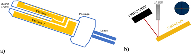
Figure 12. (a) Schematic of a tuning fork resonator and (b) cantilever resonator sensor with optical detection.
Download figure:
Standard image High-resolution imageMicrocantilever sensors
A microcantilever is typically 100 μm or so in length and 20 μm wide, smaller than cantilevers used in commercial AFM scanning probe microscopes. They can operate in static mode where the deflection is measured or in vibration mode where the change in resonant frequency and damping effects are measured. The effect of adsorbed mass and changes in surface stress are related to resonant frequency and deflection, respectively.149 An excellent review paper has been published by Boisen et al.150
The sensor response to mass changes can be represented as follows:

where Δf is the change in frequency produced by the adsorbed mass, Δm, in the presence of the analyte, fn is resonant frequency of the "nth" mode for the resonator, and me is the effective mass, also known as dynamic mass of the resonator. The mass detection can be made exquisitely sensitive by scaling down the dimensions of the resonators to nanometer range.151 The exquisite sensitivity approaching zepto-grams has been demonstrated in the laboratory. In addition, recent work has shown very high resolution when the NEMS resonator is operating at high frequency and has been studied for mass spectrometry on a chip, where arrays of resonators are used.152 Very sensitive detection of energy and surface reactions, for example the adsorption of mercury vapor, by Thundat153 and trinitrotoluene with heat of reactions by Pinnaduqage et al.154 have been shown. Microcantilevers are also very sensitive to temperature changes and some of the early work examined heat of reaction at a catalytically active surface of the cantilever since the resonators are excellent for sensitive calorimetry. Photo-thermal spectroscopy for detection of explosives and organic vapors has been very successful for detection of trace compounds, where the infrared induced adsorption is a function of the analyte functional groups on the cantilever.155 The use of high surface area materials, including CNTs has been proposed and studied for the detection of explosive vapors where the CNT network is grown in situ.156
The minimum detectable mass is related to the quality factor of the resonators, and also limited by instrumentation noise in the measurement system. An excellent discussion of noise in AFM is provided by Voigtlander157 and nanomechanical noise limits by Roukes.158 As the resonator is scaled to smaller dimensions, the frequency is increased and Q factor may be reduced due redistribution of the thermal energy between different frequency components and effects of fluid damping as analyzed by Sader.159
Methods for transduction of cantilever deflection have been based upon optical lever arm, using active electronic devices, piezoelectric films, piezoresistive strain gauges or capacitive sensing. Figure 13a shows principle of cantilever sensor in which an embedded piezoresistive strain gauge is defined in the silicon cantilever. Using silicon on insulator (SOI) wafers allows the strain gauge to be formed in a single crystal silicon layer, which is off-set from the neutral axis. The device is coated with a Metal Organic Framework (MOF) film on one surface so that the expansion of the film, when analyte adsorption takes place, gives rise to a deflection of the cantilever and hence a change in resistance.160 Figure 13b shows a disk resonator which vibrated in-plane and utilizes thermal excitation and piezoresistive sensing.161
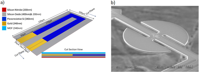
Figure 13. (a) Schematic diagram of MOF-coated piezoresistive cantilever vapor sensor, (Reproduced with permission from Ellern et al.160 and (b) SEM micrograph of disk resonator. (Truax and Brand161).
Download figure:
Standard image High-resolution imageAnalyte adsorption into the nanoporous framework of the MOF film produces changes in stress. A MOF-coated cantilever with HKUST-1, which is reversible and responds to water vapor, hexane and chloroform has been demonstrated.160 The induced stress can produce cantilever deflection according to Stoney's formula:
where L is the length, t is the thickness of the cantilever, E is the Young's modulus, ν is the Poisson ratio and δσ is the differential surface stress. Other approaches to stress-based sensing include nanoporous cantilevers formed with anodic alumina films which have arrays of pores.162 They demonstrate deflection because of adsorption of compounds due to changes in the surface energy. In addition, studies of ZIF-8 MOF-coated cantilevers show some selectivity between different compounds.163 Making simultaneous measurements of adsorbed mass and cantilever bending, which occur at low and higher concentration levels, respectively, enabled identification of different adsorption sites in the film. In addition to static deflection, the time constant associated with desorption was different for each compound, e.g., methanol, ethanol, and 1-propanol. Here the nanoporous framework could potentially be tailored for specific analyte selectivity.
Sensor functionalization, arrays and data analysis
A very thin layer of polymer film is preferred for gas sensing applications and one of the issues that has slowed the commercialization of cantilever sensors is providing a reproducible coating thickness for the polymer film. The response function is of the Langmuir type. Accordingly, the resonance frequency shifts linearly at low concentration levels, with the analyte concentration below the saturation level. Coating of the resonator with a reproducible adsorption layer is a critical issue in obtaining reproducible sensor response characteristics. A review of MEMS resonators for olfaction and biosensing is presented in.164
Cantilever sensors are typically used in arrays, so that a reference cantilever response is compared to the functionalized cantilevers. In addition, cantilevers in an array can be functionalized with different coatings to provide selective response and mimic olfaction sensing by using pattern recognition for identification of the compounds present. However, these methods are susceptible to changes in calibration with aging of the sensing film and need to use principle component analysis or other forms of neural networks for the identification of the compounds in a mixture.165
Examples of novel resonators for chemical and biosensing
Other novel mechanical resonators have also been used for chemical and biological sensing. A particular type of these resonators is a capacitive micromachined ultrasonic transducer (CMUT), which has been originally developed for air-coupled applications and medical imaging.166 Recently, CMUTs have been used for gravimetric chemical sensing.167 Compared to other mechanical resonators, CMUTs offer several advantages that include multielement structure on a single die, multicell construction of a single element, easy integration with electronics, fine mass resolution, and fast response.168 The recent efforts to miniaturize CMUT-based sensors have produced a complete battery-operated, wireless, multidimensional sensing system.169 The capacitive micromachined ultrasonic transducer (CMUT) is essentially an electrostatically-actuated flexural mode microelectromechanical resonator. Anodic bonding can be used to fabricate a CMUT with the structure shown in Fig. 14a.170 A sub-micron cavity is formed in a borosilicate glass substrate by first etching to facilitate a high electric field strength, which is key to achieve a high electromechanical coupling; then an electrode (Cr/Au) is patterned in the cavity; and followed by a silicon-on-insulator (SOI) wafer anodically bonded on top to form a vibrating thin plate. Gold is deposited on the top of the plate, serving as the top electrode as well as to provide a suitable surface for further functionalization steps. The resonant characteristics of the vibrating thin plate are mainly determined by its mechanical properties and physical dimensions. More specifically, the first resonant frequency of a stress-free circular plate is given as:
where E, ν, and ρ are plate material's Young's modulus, Poisson's ratio, and density, respectively, and t and a are the thickness and radius of the plate, respectively.

Figure 14. (a) The basic building block (cell) of a CMUT fabricated using anodic bonding on glass substrates. (b) Multiple cells connected electrically in parallel make up an element. (c) Several elements can be placed on the same die to make a multichannel sensor array.
Download figure:
Standard image High-resolution imageIn typical applications, a high DC-bias voltage is applied between the top and bottom electrodes to narrow the gap. A large number of the vibrating thin plates (cells) are electrically connected in parallel to form a single CMUT element (Fig. 14b). This structure has several advantages over a single-cell structure: (1) improved noise performance by the square root of the number of cells,171,172 and (2) better capture efficiency due to larger available sensing area. In order to offer the capability of discriminating between multiple analytes, multiple CMUT elements are formed on a single die (Fig. 14c). Then, the individual sensing elements are coated with various polymers using techniques such as drop casting, spray coating, or inkjet printing. One element can be left uncoated to be used as a reference to track the effects of factors that are not due to chemical exposure, such as pressure, temperature, and humidity. CMUT-based sensors have been used to detect chemical warfare agent simulant dimethyl methylphosphonate (DMMP),173 carbon dioxide,174 volatile organic compounds as environmental pollutants,175 plant volatiles as stress indicators,176 and as an electronic nose to differentiate between different types of coffee beans.177
These types of mechanical resonators, as the cantilevers, exhibit a lower quality factor when loaded by a liquid medium. Functionalizing the surface of the sensor with agents such as antibodies enables detection of biomolecules. Novel synthetic antibodies show a lot of promise for selective detection in a complex media.178 However, the lower quality factor in liquid media poses challenges for operation with biological fluids. One way to address this challenge is to introduce the sample in liquid form and perform measurements in air after drying the surface to get the benefit of higher quality factor. A selective human immune protein immunoglobulin G (IgG) sensor has been demonstrated this way using the hexamer peptide ligand HWRGWV for functionalization179 CMUTs can also be designed with pressure release boundary condition in close proximity of the membrane to enhance the quality factor in immersion.180
Another way to address the challenge of sensing in biological fluid samples is to introduce the sample through a channel embedded in the resonator structure, so that a high quality factor can be achieved. In this case, the surrounding medium can be vacuum to improve the quality factor even further. An example of this approach is the suspended microchannel resonators, which are microfluidic channels, embedded in microcantilevers. The biological fluid sample continuously flows through the microfluidic channel and delivers biomolecules, cells or synthetic particles. The cantilever is packaged under high vacuum and the wall and fluid layer thicknesses are shrunk to the micrometer scale to attain sub-femtogram mass resolution.181,182 A similar approach has also been proposed for CMUT-based sensors.183
Future prospects
Many types of transduction methods have been exploited for chemical sensing with resonators, and they all share the unique characteristic that a frequency counting provides a high degree of reproducibility and accuracy. In most cases, the primary application of the resonator is not chemical sensing but a frequency reference or acoustic sensor, however, through miniaturization the cost of these devices has been reduced, so that arrays of devices can be deployed with different coatings or operating at different temperatures for example. Novel materials for resonators including GaN make use of a semiconductor, which is both, piezoelectric and piezoresistive, allowing integration of the sensing and electronics. Parametric resonance and Duffing oscillation of resonators for greater sensitivity to mass changes is also a new direction for study.
Applications of electronic nose systems in environmental monitoring, industrial process control, pharmaceuticals, food science and technologies, biosecurity, disaster recovery, forensics, military operations, law enforcement, transportation safety, and scientific research have been known for a long time. In addition to these there are many promising emerging applications of the electronic nose technologies enabled by the lower cost, increased reliability, higher power efficiency and smaller form factor of the new generation of sensors. These sensors will enable the distributed sensing required in the internet of things (IoT) settings. Air quality monitoring in smart buildings and cities, humidity control in food storage, wearable gas sensing for monitoring individual exposures especially in occupational settings are some examples. Furthermore, applications in health care for detecting trace amounts of volatiles in breath as well as emitted from the skin surface will enable early diagnosis for many diseases by discovering new gas-phase biomarkers. These sensors can be integrated as part of point-of-care diagnostic devices or monitoring systems at home. Some other future applications are in food safety. Diseased and contaminated plants as well as microbes emit specific volatile signatures. Low-cost selective chemical sensors that can be strategically placed across crop fields, orchards, greenhouses, food processing facilities, and storage can help detect contaminated plants and crops.
Sensor Arrays
Often a gas sensor problem is not solved by a single sensor alone. Thus, combining individual sensor elements into a sensor array is a standard aspect of the gas sensing field. The discussion below gives an overview of gas sensor arrays.
Core technology
Development of sensor arrays for chemical detection and analysis has been an active area of research for more than 30 years, with numerous published reports of these devices collectively demonstrating their utility in a wide range of applications.184–190 Arrays of non-specific chemical sensors are often referred to as "electronic noses," although the applications are not limited to tasks in machine olfaction or vapor sensing. Classically, these devices consist of co-located arrays of individual chemical sensors that exhibit independently varying sensitivities across a domain of possible analytes and provide an aggregate response that is used in conjunction with some chemometric modeling approach to infer chemical information about the sensed environment. Sensor arrays can be constructed from collections of similar sensor types that are each functionalized differently or collections of widely different sensor modalities. More recent work has moved towards development of strategies in which an individual sensor provides multiple "channels" of information rather than physically distinct co-located sensors. This is accomplished via tunable selectivity191 or the extraction of multiple sensor response variables.192 All of these approaches can themselves be combined in various permutations, leading to varying levels of capability and data complexity. In practice, array configuration options are limited by sensitivity, selectivity and stability requirements, as well as logistical constraints imposed by the intended use case and availability.
Persaud and Dodd are generally credited with the first published description of a chemical detection system based on an array of chemical sensors with overlapping sensitivities.193 The array described in this work consisted of three commercially available gas sensors based on tin-oxide semiconductors. Although each sensor was intended by the manufacturer to sense a different class of compounds, the authors noted that significant cross-sensitivities to analyte vapors existed between the sensors. They proposed that this technology could thus be used as an analogous means to study discrimination mechanisms in mammalian olfaction, which was known to rely on an array of broadly tuned olfactory receptor neurons. This is the key insight that underpins all sensor array research and development: diverse partial selectivity among sensors enables construction of arrays that exhibit analytical capabilities beyond those possible from individual sensors.
Other examples of such devices were published shortly thereafter, including arrays of metal oxide sensors, amperometric sensors, quartz microbalances and surface acoustic wave sensors, as well as early considerations of the potential limitations and capabilities of this technology.194–202 Since this initial period, this field of research has continued to grow, with numerous articles published in the literature each year. This body of literature includes sensor arrays representing all major categories of sensor technologies. Reviews of sensor array research are published regularly, and generally focus on specific sensor technologies or application areas.184–192,203–220 Hierlemann and Gutierrez-Osuna provided a particularly comprehensive discussion of issues surrounding sensor array technology in their 2008 review, "Higher Order Chemical Sensing."207
Commercially available chemical detection systems based on sensor arrays appeared within a decade of the earliest literature reports and quickly increased in ranks, with a dozen or more vendors populating the market since 2000.188,189,210,221,222 However, there has also been persistent disenchantment with these devices: possibly from tendencies towards overestimation of the capabilities of sensor arrays, underappreciation of the complexity of the sensing tasks to which they have been applied, a general lack of systematic design and validation principles, and the poor stability and robustness of the sensors used.192,223–226 The net result is that while turnkey sensor array devices persist in the marketplace today, they do so as products for niche applications rather than as more general-purpose analytical tools.
Sensor design and detection mechanism
A salient characteristic of these systems is that the sensor responses are intended to be used in aggregate to provide an analytical result. In other words, there is not a "one-to-one" correspondence between sensor and analyte. Instead, each sensor generally exhibits significant cross-sensitivity over a range of chemical compounds, as in biological olfaction. The intent is that the individual capabilities of each sensor in an array will complement each other in an analytically-relevant fashion. As noted in,192 cross-sensitivity is general feature of chemical sensors due to a fundamental trade-off between selectivity and reversibility in sensor transduction mechanisms. Combining multiple partially selective sensors is desirable as a means of broadening the range of addressable target analytes or chemical signatures without having to employ more complex analytical instrumentation. This approach also offers the possibility of mitigating the impact of interferants and other environmental conditions. In this sense, sensor arrays can be viewed as a logical intermediate between individual chemical sensors and multivariate, spectral instruments in terms of information-generating capacity.
A central challenge in realizing the potential of this approach lies in array design and optimization. The combinatorial nature of the problem can mean that even a modestly sized pool of candidate sensors and target analytes could result in a substantial number of possible array configurations and potential sensing tasks. This renders "brute force" empirical optimization of sensor array configuration impractical or impossible. Thus, sensor array design should be informed by an understanding of how information flows through these systems as well as by an understanding of the parameters of the sensing tasks to be accomplished. Unfortunately, theoretical consideration of sensor array design and sensor array capability are relatively underreported in the literature.227
Zaromb and Stetter considered sensors arrays as a system of equations comprised of linear sensor response functions.194 The immediate implication is that an array with N sensors is limited to simultaneous determination of N or fewer analytes, although the authors note that this limitation could be mitigated if only a small amount of analytes are expected to be present at a given time. The determinant of the matrix of response coefficients for a given collection of sensors applied to given set of analytes is presented as a measure of the selectivity. It is inversely proportional to the expected error in estimating analyte concentrations and is proposed as an optimization criterion for selecting among multiple candidate sensor configurations for target analyte sets.
Later, Gardner and Bartlett use a similar mathematical framework to describe sensor arrays as a mapping between two geometric spaces, one describing the span of all possible analyte mixtures (the sample space) and the other describing the span of all possible sensor array responses (the measurement space).228 Using this framework, an approach to propagating sensor measurement error to the sample space for specific sensor array configurations and sensing tasks was shown. This allowed calculation of a hyperellipsoid error volume element in the sample space, and from that, a nominal maximum number of resolvable analyte mixtures, thus providing a measure of information-generating capacity.
Pearce and Sánchez-Montañés subsequently demonstrated an approach in which analyte determination with a sensor array is treated as a statistical estimation problem.229–231 The Fisher information matrix calculated from a statistical model of the sensor response functions is used to provide, via the Cramer–Rao bound, a covariance matrix that is the lower bound of the estimation error exhibited by a sensor array. While this measure does not necessarily provide an estimate of the actual error one would incur with a given sensor array, as a lower bound to this error it does offer a measure of the fundamental capability of that system to provide analytical information that is independent of the particular data analysis strategy employed. The determinant of this covariance matrix provides a lower bound on the hyperellipsoid error volume described by Ref. 228. Johnson and Knapp later described the connection between classic notions of analytical selectivity and Fisher information-derived measures and proposed a corresponding sensor array selectivity measure.232 This work also suggested that minimization of Fisher information-derived marginal error bounds associated with particular analytical tasks may provide more useful optimization criteria than maximization of the proposed selectivity measure.
It is important to differentiate between analytical figures of merit for individual sensors and those of a sensor array formed from them. The fundamental capability of a sensor array lies in the existence of a bijective mapping between the span of potential analyte mixtures and the span of possible array response vectors, enabling array response to uniquely determine mixture composition. In practice, measurement error degrades this capability and renders, to some degree, the responses from similar mixtures indiscernible. The extent to which measurement error impacts the analytical capability of an array is dependent on the magnitude of the measurement error of each sensor, the magnitude of the sensitivity to each analyte, and the similarity between the response functions of the two sensors. The first two factors together provide a base measure of signal-to-noise while the third provides a measure of selectivity, which modulates how this signal-to-noise measure translates to sample estimation, or resolving capability between mixtures of different composition.
A sensor array exhibits a sensitivity for each analyte that is the geometric sum of the individual sensor sensitivities on the measurement space of the array. In this way, two sensors that both respond to a given analyte augment each other to provide an array with effectively greater sensitivity to that analyte. Likewise, measurement error is defined as a multi-dimensional joint distribution for the array and as one-dimensional distributions for each sensor. In the case that the error distributions of the sensors are independent, the array measurement error is the product of the individual sensor distributions. Definitions of selectivity are generally grounded in a semi-quantitative notion of "the degree to which a measurement system provides a unique response" to one analyte vs others.233 This definition leads to a natural tendency to place selectivity on a scale between two extremes: non-selective and fully selective or specific. Intermediate values are referred to as "partially selective." Specific sensors respond to only one target analyte, while partially selective sensors respond to multiple analytes, but with distinct response functions. Non-selective sensors respond identically to multiple analytes. Selectivity for sensor arrays can be defined in an analogous fashion using a measure of similarity in multivariate response.234 For example, for an array of linear sensors, one could calculate the cosine of the angle between the array response vectors to two different analytes. Orthogonal responses (cosine equal to zero) represent maximum selectivity while collinear responses (cosine equal to one) represent minimum selectivity.
Sensor array selectivity is important because it modulates the analytical capability of the array to determine one analyte in the presence of an uncertain amount of another analyte. From a geometric interpretation, it can be shown that as the sensor response patterns become more similar the proportion of the response that can be used to uniquely determine each analyte (referred to as "net analyte signal" in chemometrics235) becomes progressively smaller. This leads to an effective reduction in signal to noise and a higher limit of detection for fixed sensor measurement error and analyte sensitivity.232–236 Alternatively, selectivity can be interpreted in a statistical estimation context as the degree to which measurement error is correlated when propagated to analyte concentration estimates.232 A fully-selective sensor array with orthogonal analyte responses will lead to uncorrelated sample estimation error. As the responses depart from orthogonality, the joint estimation error distribution in the sample space is distorted in a manner that reflects the increased difficultly presented in discerning one analyte from another, but also increased composite sensitivity for mixtures of the two analytes conferred by response overlap between analytes. Thus, an array that presents lower selectivity between two analytes will generally perform more poorly at simultaneous estimation of two unknown analytes and be less capable of discerning between different mixtures of the two analytes. However, such an array may also be more effective at accurately estimating the concentration of a chemical signature comprised of a fixed ratio of those analytes.
Fonollosa, et al. have also explored the use of information-theoretic measures such as mutual information for optimization of sensor arrays and characterization of olfactory systems.237,238 Mutual information quantifies the amount of information one random variable conveys about another.239 The quantity is minimized when the two variables are completely independent and maximized when one variable is exactly correlated to the other. In this approach, both marginal and joint probability distributions must be estimated over the domain of sensor responses and analyte concentrations. The optimal sensor array configuration maximizes mutual information. Because this approach incorporates explicit probabilistic information regarding the analyte vapors, it enables direct optimization to situations involving a collection of random sensing tasks on a known library of potential analytes, and particular facility in describing problems involving detection statistics such as limit of detection. However, the optimization criteria it provides may be less directly interpretable in the context of other traditional analytical figures of merit and can rapidly become unwieldy with increases in the dimensionality of the configuration problem and the resolution with which sensor responses and analyte concentrations are specified.
The sensor array quality measures discussed above are inferred from statistical models of sensor response functions or comparison of stimulus and response distributions, and thus enable optimization of sensor array configuration according to theoretical information-generating capability. In practice, chemical information is usually derived from sensor arrays via chemometric regression or pattern recognition models applied to the multivariate sensor array output.240–244 These models are formulated with calibration data and/or known functional relationships between analyte concentration and sensor response. Empirical measures of model prediction precision and accuracy such as root mean square error of prediction or classification rate and ROC curves are routinely used to evaluate system performance. Error rates can thus be compared to informational capability measures, providing a measure of the efficiency of the chemometric approach used.
Finally, it should be noted that sensor arrays experience unique issues in data quality and data preprocessing requirements. For example, if an array is constructed of widely different sensor types, scaling and normalization of the sensor response data may be necessary to prevent one or more sensors from inappropriately dominating the output of the array. As with individual sensor applications, sensor malfunction and drift in response can be a serious issue. In particular, response drift both alters the fundamental capability of the array and de-calibrates the chemometric prediction models applied to the data. This is exacerbated by the fact that in an array, drift can vary independently among sensors, making it more difficult to algorithmically correct and progressively more impactful as the number of sensors in the array increases.192 On the other hand, sensor arrays also offer unique possibilities for recognition and correction of sensor error through strategic incorporation of redundancy in response.
Sensor response and example structure
The simplest sensor array example is a combination of two partially selective sensors to successfully determine two target analytes. This is not particularly uncommon. For example, commercially available electrochemical carbon monoxide sensors commonly exhibit significant cross-sensitivity to hydrogen.245,246 This becomes problematic in applications where both gasses may be present and one wishes to independently assess the concentration of both analytes. One avenue to address this deficiency is to couple a carbon monoxide sensor with a hydrogen sensor and use the responses of both to correct for the influence of this cross-sensitivity. Suppose one manufacturer offers carbon monoxide and hydrogen sensors with linear response and relative cross-sensitivities to the other analytes of 40 and 20 percent, shown below in Table II as sensors A and B. Alone, either sensor presents at best an indication that at least one analyte is present but complete ambiguity as to whether a mixture is present, let alone the relative concentrations of each analyte. Clearly, combining the two sensors enables simultaneous determination of both analytes, even though both exhibit partial selectivity. However, suppose there are two other sensors available: carbon monoxide and hydrogen sensors with relative cross-sensitivities of 20 and zero percent, listed in Table II as sensors C and D.
Table II. Candidate pool of carbon monoxide and hydrogen sensors.
| Relative Sensitivity | ||
|---|---|---|
| Sensor | CO | H2 |
| A | 1.0 | 0.4 |
| B | 0.2 | 1.0 |
| C | 1.0 | 0.2 |
| D | 0 | 1.0 |
One might ask, what are the relative merits of replacing sensor A with sensor C vs replacing sensor B with sensor D? How does an array consisting of sensor A and B compare to one consisting of sensor C and D? Table III below summarizes several quality measures (as described in233) for various configurations of the sensors presented in Table II. For example, we see that replacing either A or B with their more selective counterparts results in increased selectivity and reduced estimation error bounds, as one might expect.
Table III. Selected sensor array configurations and corresponding quality measures: array selectivity, marginal error bounds for carbon monoxide and hydrogen detection, and generalized error bound in the joint sample space. Measures are calculated assuming sensors exhibit Gaussian error with unit variance, and unit sensitivity to the intended target analyte.
| Configuration | Selectivity | CO Error Bound | H2 Error Bound | Gen. Error Bound |
|---|---|---|---|---|
| A,B | 0.70 | 1.37 | 1.23 | 1.18 |
| C,B | 0.85 | 1.13 | 1.13 | 1.09 |
| A,D | 0.90 | 1.11 | 0.99 | 0.96 |
| C,D | 0.96 | 1.04 | 1.00 | 1.00 |
| A,C | 0.10 | 5.00 | 50.0 | 25.0 |
| B,D | 0.50 | 50.0 | 1.00 | 25.0 |
| A,B,C,D | 0.86 | 0.57 | 0.53 | 0.26 |
However, there are several more interesting phenomena to be noted here. First, while an array comprised of sensors C and D offers higher selectivity than any of the other two sensor arrays, it does not decrease the estimation error bound for hydrogen nor does it decrease the generalized error bound in the sample space. This is because sensor A exhibits higher sensitivity for hydrogen than sensor C and thus shrinks the marginal estimation error for hydrogen enough to compensate for increase in error induced by the increased correlation. Second, it can be seen that the partial selectivities of sensors A, B, and C enable arrays composed of the two carbon monoxide sensors (A and C) or the two hydrogen sensors (B and D) to exhibit a collateral capability to sense the other analyte. However, this capability is greatly reduced, exhibiting significantly lower selectivity and an estimation error bound that is approximately fifty times greater than those of the other two-sensor configurations. Finally, an array comprised of all four sensors exhibits marginal estimation error bounds that are nearly half those of the best-performing two sensor arrays but with lower selectivity. The general effect of adding sensors to an array while considering a fixed set of target analytes is both an increase in average sensitivity and a decrease in selectivity. The former because the array sensitivity is the geometric sum of the individual sensor values; the latter because, as more sensors are added, there are less ways in which the sensors can be "unique" with respect to the target analytes.
It should be noted that this example involves sensors that are assumed to exhibit similar sensitivity to their respective primary analytes and fixed, unit variance Gaussian measurement error. One could also examine the impact of incorporating alternate sensors with varying measurement error and absolute sensitivities with this approach. In general, increases in sensitivity reduce estimation error bounds in some fashion, while increases in measurement variance increase them. Non-linear sensor response functions can be considered, although this leads to concentration dependence in these quality measures, as would consideration of concentration dependent measurement variance models. Finally, although marginal error bounds are only shown for individual analytes in Table III, these can be determined for arbitrary orientations in the sample space, and thus for arbitrary sensing tasks. These concepts scale to more complex examples with larger arrays and analyte sets. The span of potential sensing tasks will increase with the number of analytes considered. For example, one could consider two complex signatures of overlapping composition, each consisting of defined ratios of a dozen individual analyte vapors.
Future prospects: critical issues, challenges, and future directions in the field
The most central challenge moving forward is to make sensor arrays more practical and reliable for complex, real-world chemical sensing tasks. These tasks can present dynamic and uncertain chemical environments that make optimization difficult and predictions of performance quality unreliable. Normally, the risks inherent in uncertain chemical analysis problems can be minimized with high-information analytical laboratory techniques, like spectroscopy or chromatographic separation followed by mass spectrometry. However, these techniques can be costly or otherwise inappropriate for sensing scenarios. They also may provide more analytical capability than necessary, and thus represent an inefficient solution in many sensing applications. Sensor arrays offer the potential to provide efficient analytical solutions to a variety of complex chemical sensing tasks, but only with an improved theoretical understanding of how sensor array design relates to sensor array capabilities and limitations. Methods must be developed to optimize capabilities for complex, uncertain sensing tasks. As with analytical instrumentation, greater uncertainty must be matched with greater instrumental complexity. Importantly, appropriate data analysis algorithms must also be selected or developed to most effectively extract the information a sensor array is theoretically capable of producing. An emphasis must be made on how knowledge regarding the parameters of a sensing task can be compiled, quantified, modeled and matched to an appropriate sensor array capability in a quantitative fashion allowing optimal sensor array configuration. Information theoretic, Bayesian, and machine learning approaches will continue to play an important part in these efforts,247–251 as they have in similar problems in communication, cryptography and neural system modeling.227,232,238,239
Next, enhanced robustness is necessary to expand adoption of sensor array approaches. Hardware and algorithmic drift mitigation strategies will continue to be critical, although largely sensor-specific. Multivariable, "virtual" sensor arrays represent a promising strategy for minimizing the impact of sensor drift on sensor arrays because the drift is correlated among the variables, and thus more easily corrected.192 Another benefit of this approach is the potential for arrays of multivariable and adaptive sensors to function as "higher order" analytical devices, able to take advantage of chemometric second and third order advantages: calibration against unknown interferants and single-sample calibration, respectively.252 A method has been proposed to perform Fisher information-based array optimization in the presence of correlated sensor measurement error using elliptical contoured distributions.253 This work also details a convex optimization strategy to enable near-optimization of larger-scale arrays in more practical timescales than simple "brute force" optimization. Algorithmic approaches to evaluating sensor array quality and calibration updating will also be important for long-term autonomous sensor array applications.
Lastly, fabrication of microscale sensing elements (for example, through inkjet printing254–256) has advanced sufficiently to make large-scale arrays with hundreds of different sensor types possible.257 This means that a central limitation on the design and capabilities of sensor arrays is the number and quality of candidate sensing materials available. New sensors designed for greater response diversity need to be developed to enable greater flexibility in array design and optimization as well as a wider range of capabilities and the potential to approach the scale of biological chemical recognition systems. Adaptive sensor technologies are particularly important in this effort, as they embrace the idea of tunable sensitivity, potentially allowing not only a large number of diverse sensors, but also the possibility of reconfiguration to optimize for new sensing tasks without replacing individual sensors. Adaptive sensors based on temperature modulated electrochemical sensors have been well-described in the literature,208,237 but any sensor technology with a controllable parameter that induces an analyte-dependent change in sensitivity could be utilized in this fashion. Alternatively, incorporation of a simple, partial chromatographic separation prior to detection could serve to modulate the array signal in time in an analyte-dependent fashion and thus enable improved analyte discrimination.258
Complimentary Technologies: Microfluidics in Gas Sensing Systems
The ability for gas sensor to operate in a given environment and solving a measurement problem is often dependent on supporting technologies. An example of these technologies is microfluidics for sampling and preconcentration. The discussion below provides an overview of microfluidics for gas sensing systems.
Core technology
Fundamentals for gas flow and sampling at the microscale
Trace gases can be volatile organic compounds,259 energetic materials260–262 or even biomarkers,263,264 which are all valuable targets for gas sensors; however, trace gas (typically considered to be <1% of the total sample volume) detection is difficult due to high variability in the specificity and detection limit of gas sensors. Concentration of trace gases prior to analysis is useful to bring their concentration within the detectable range, while also increasing the accuracy of the measurement. Accordingly, there have been significant efforts to design and validate gas-sampling microfluidics for integration into "lab-on-a-chip" devices for miniaturized gas chromatography265–268 environmental sensing269–271 and point-of-care diagnostics.272–274
Research in the area of microfluidics has typically focused on the control and manipulation of liquids; nevertheless, at the microscale (<100 μm), the effects of gravity are negligible and viscous forces become the major player in determining flow of both liquids and gases. Inertial forces at the microscale are derived from the velocity of the fluid, while the viscous forces are derived from the viscosity of the fluid. A Reynolds number (Re), i.e. the ratio of inertial forces to viscous forces, greater than unity indicates that velocity dominates the flow; whereas, Re less than unity indicates that the flow is dominated by viscous effects. For most liquids and gases, Re is greater than unity, but since this ratio is also dependent on the size of the conduit, Re can be manipulated via the design of microfluidic channels and devices. The design of the microfluidics can be employed to generate stokes (Re < 1), laminar (1 < Re < 2000), transitional (2000 < Re < 4000), and turbulent (Re > 4000) flow. At the microscale, liquids are usually stokes or laminar, while gases exhibit transitional or turbulent flow.
Gases can easily transition into and maintain turbulent flow, even at the microscale, due to low viscosity and relatively high velocity. While detrimental to many liquid handling processes, turbulent flow is of particular necessity for gas sensing. Under laminar conditions, fluid boundary layers have a "no slip" condition meaning there is no gas flow or convective exchange of molecules at that boundary, i.e. the wall of the microchannel or surface of the gas sensor. Since this boundary is where both the sensors' recognition and transduction occur, laminar flow reduces the volume of sample that interacts with the sensor; therefore, the sensitivity and limit of detection are negatively impacted. Gas sensor performance can be improved actively mixing and introducing the gas to the sensor's surface via turbulence. By simply employing microfluidics, the gas samples will experience convective exchange at the sensor's surface; however, the utility of turbulent flow for gas sampling has to be precisely balanced with the necessary residence time for the sensor. Since turbulent flow of gases requires relatively high flow rates, residence time will be decreased. For that reason, there is a growing body of research, which explores the design of microfluidics to both exploit the inherent mixing in turbulent flow and contribute preconcentration capabilities, which will improve the performance of sensor systems.
Designs and examples
Microfluidic preconcentration
In the case of trace gases, or gases whose concentrations are below an instrument's detection limits, concentration of the sample is required to enable accurate and precise quantification of the desired analyte. Concentration of the analyte typically occurs upstream of the analytical instruments; therefore, such processing steps or devices are called preconcentration or preconcentrators, respectively. Preconcentration of analytes is performed via myriad methods—including extraction, physisorption, precipitation, distillation, filtration and centrifugation (Fig. 15).275 Gas preconcentrators typically involve either extraction, physisorption, or precipitation. Both extraction and precipitation may result in chemical changes to the analyte; moreover, both methods require "off-line" processing and separation steps. Physisorption is the predominant method applied to microfluidic preconcentration; physisorption is the accumulation of analyte gases on adsorbing materials, i.e. sorbents, at low temperature, and the subsequent release of high concentrations of gases through desorption by controlled heating or chemical elution. Sorbents are solid-phase materials that either absorb or adsorb the gas analyte of interest. Using either passive (diffusive) or active (convective) sampling, the sorbent immobilizes the analyte, which can then be desorbed into a carrier gas by thermal or chemical processes.276 Herein, we briefly introduce microfluidic preconcentrator technologies for gas sensing, and how these systems improve the sensitivity or selectivity of the gas sensors.

Figure 15. Schematics of microfluidic preconcentrator sorbent material packing and deposition strategies. (a) A capillary with a thin film deposited on the wall. (b) A capillary with a packed bed of granular sorbent material. (c) A microfluidic channel with a thin film deposited on the walls. (d) A microfluidic channel filled with granular sorbent material. (e) A microfluidic array either (f) coated in a thin film, or (g) packed with granular sorbent.275
Download figure:
Standard image High-resolution imageMicrofluidic preconcentration of gases can be categorized by the type of sorbents employed: (1) mesoporous ceramic powders, (2) activated carbon, or (3) designer nanomaterials.277,278 The sorbents define the minimum period for gas adsorption to accumulate the necessary concentrations of the analyte; moreover, the sorbents can provide further discrimination, when they desorb at different temperatures or when the gases are separated using consecutive micro-columns.275,279 Figure 16 illustrates the differences of these materials, while also highlighting some of the common strategies of microfluidic preconcentrators. These strategies include coated and packed capillaries, coated and packed channels, and coated and packed arrays.275 The preconcentration factor is the standard measure of how well the preconcentrator adsorbs and releases the analyte. While there is some variance in how this can be reported, the easiest way to evaluate it is in the ratio of the peak concentration in the desorbed volume divided by the peak concentration in the sample volume (without preconcentration). Simply put, a highly efficient preconcentrator will convert a wide chromatographic peak at a very low amplitude and concentrate it into a very narrow chromatographic peak with a very high amplitude.
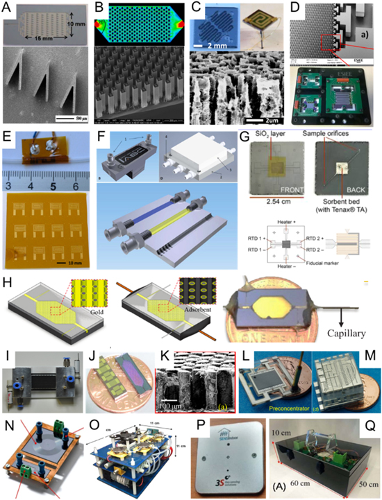
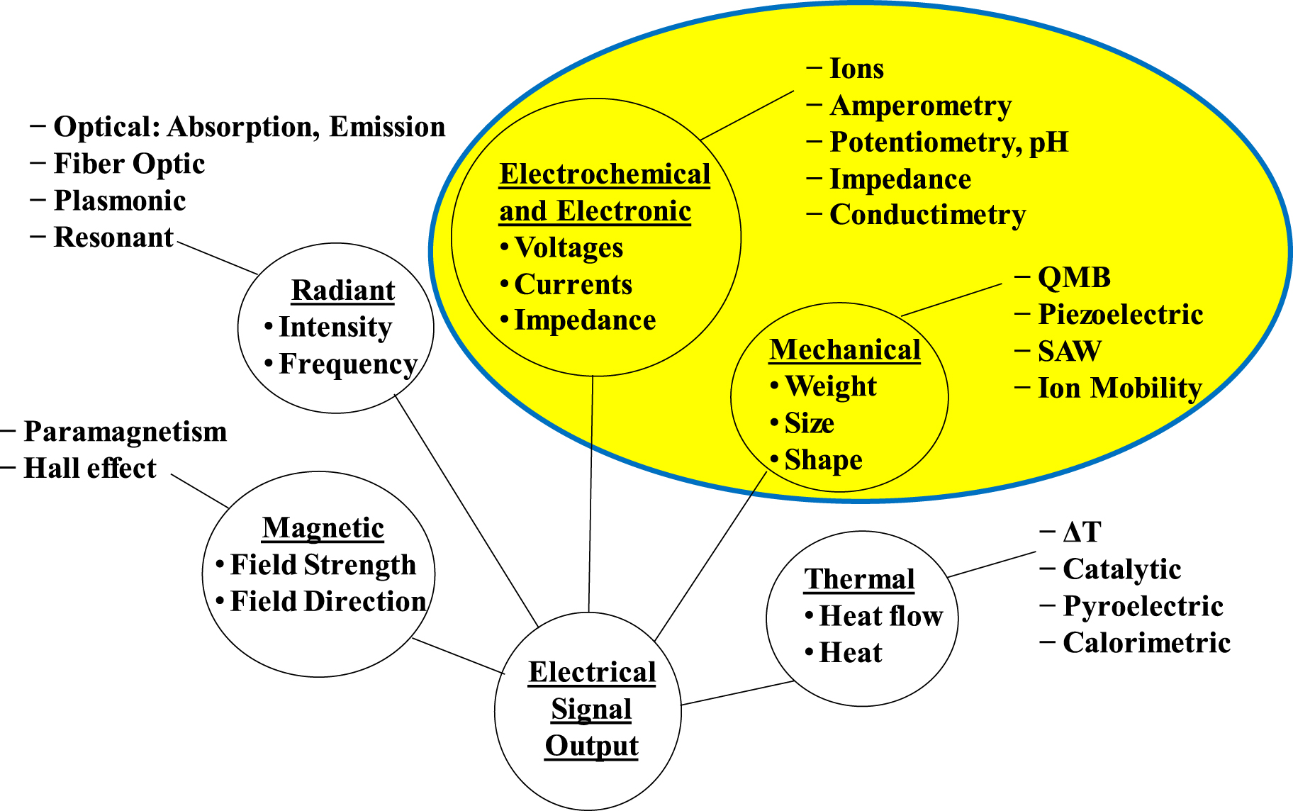
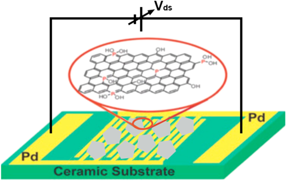
Figure 16. Examples microfluidics integrated with gas sensing systems. (a) Gas manifold etched in silicon, along with an electron micrograph of etched structures to increase surface area279 (b) Flow simulation and electron micrograph of etched pillars to increase surface area.280 (c) Serpentine preconcentrator packed with sorbent and backside microheater.281 (d) Manifold device with pillars integrated into a gas sensor package.282 (e) A tubular preconcentrator device comprised of a microheater printed on a film and rolled around a sorbent.283 (f) Illustrations of a miniature gas cell with a thin film sorbent coating.284 (g) A preconcentrator fabricated in glass using non-DRIE methods.285 (h) Preconcentrator with gold microheaters deposited directly within the microchannels.286 (i)–(k) Large capacity preconcentrator filled with carbon-based sorbents and sorbents generated by in situ firing of cellulose.287,288 (l) The preconcentrator stage of a complete gas sensor system.289 (m)–(q) Complete gas sensor systems with integrated microfuidics and preconcentrators for volatile organic compounds290 biomarker detection,291,292 and environmental gas sensing.293,294
Download figure:
Standard image High-resolution image
To describe the basic features of microfluidic preconcentrators, we will evaluate the Camara et al. demonstration from 2010.279 They have designed multiple preconcentrators to elucidate the effect of the internal geometry on the preconcentration factor. All of their microfluidic preconcentrators were fabricated in silicon by dry reactive ion etching (DRIE). Fabrication by DRIE is a very popular method for creating gas-tight, chemically robust housings for the sorbents and conduits for gas flow.295 Camara et al. also increased the surface area of the device by wet etching in a hydrofluoric acid bath to generate interconnected pores. This process turned a single inlet to interconnected branches, effectively increased the quantity of sorbent that could be incorporated and pathlength of the resident gas, which then increased interaction with the incorporated sorbent. A screen-printed, platinum microheater was attached to the preconcentrator for thermal desorption of analytes. The best preconcentration factor reported for benzene was 64, which brought a sample concentration of 250 ppb up to about 16 parts per million (ppm).279 Subsequent microfluidic preconcentrator designs have been reported, and most detail the use of DRIE to fabricate complex channels to increase the quantity and surface areas of the integrated sorbents.280–282 Typically, such microfluidic preconcentrators are able to increase the analyte concentrations from ppb to ppm, when applied to the analysis of both volatile organic compounds and biomarkers. Such increase in concentration via passive means may revitalize sensor designs and motifs that have been thought to have lesser capability.
Alternatives to DRIE-patterned microfluidics
Alternative manufacturing methods are gaining popularity for the fabrication of microfluidic devices. Additive manufacturing, computer numerical control (CNC) milling, hot embossing, and printing techniques are necessary to shift microfluidic technologies from "lab-only" to "distributed" markets. The fabrication of a tubular microfluidic preconcentrator by inkjet printing has been reported.283 The microheater, sorbent, and interconnects can be directly printed onto a substrate or device. In the cited example, the microheater was printed directly onto a packed sorbent column, and with this device geometry, gas flow can reach 4.5 l·min−1 without mechanical failure. A very short adsorption time of 5–120 s was reported. In comparison to convention DRIE-fabricated microfluidic preconcentrators, benzene, toluene, nitrobenzene, and acetophenone were processes to similar preconcentration factors but with a two order of magnitude improvement in adsorption time (5 s vs 5 min). Kokoric et al. reported a miniaturized version of a traditional gas cell with incorporated sorbents that was directly machined from aluminum.284 This preconcentrator provided for either parallel or series analysis of single and multiple gas flows. Each conduit can be filled with a different sorbent and multiplexed separation and analysis can be achieved. While the device is direct in design, a very high surface area of sorbent was achieved small footprint—≈500 μl of flow volume. While high-capacity silicon devices have flow volumes of approximately 50–100 μl. Another interesting design factor is that optimal adsorption in carbon sorbents occurs below room temperature; therefore, the rate of cooling and heating is improved by using the aluminum substrate. Another fabrication method that does not use DRIE has been reported recently by McCartney et al.285 The two pieces are bonded together via thermal fusion bonding yielding a sorbent region with a flow volume of about 70 μl.
In addition, the improved integration and thermal coupling of microheaters enable the rapid desorption of analytes promoting better chromatographic separation, preconcentration and resolution.281,282 Microheaters are also being integrated directly into the microfluidic preconcentrator or devices. Kuo et al. have developed both a preconcentrator and a separation channel with heaters built into the channel structures as opposed to being sputtered on the backs of a device.286 They report a heating rate up to 75 °C s−1 and preconcentration factors for toluene and xylene greater than 7900. This is a significant improvement in microfluidic preconcentration technology that allows for more robust temperature control.
Future prospects
While gas sensor systems are dependent on the sensor design and performance, complimentary sample-handling and sample-processing technologies will improve both sensitivity and selectivity of the overall system. We have briefly illustrated the possibilities for incorporating microfluidic gas handling into sensor system, and we would point towards current reviews in the area of breath sensing262 and microscale chromatography265 for more in-depth examination of these techniques. There is also significant design and engineering effort being dedicated to improving the operation of microfluidics and gas sorbent systems. Towards increased capacity, Janssen et al. developed an eight-channel large capacity manifold that has a sorbent volume region of about 576 μl.296 For sorbent selection, cellulose has been successfully turned into activated carbon after in situ firing at >500 °C.287,288
Concerning microfluidic preconcentrators, the evolution from traditional fabrication techniques, e.g. DRIE and photolithography, to additive manufacturing technologies, e.g. inkjet and 3D printing, is promising for the future integration and miniaturization of gas handling devices. Total gas analysis systems are being fabricated with footprints smaller than the American penny.289,290 Breathe analysis for lung cancer screening are only a few steps away from clinical testing.291,292 Environmental atmosphere sensors are being commercially deployed.293,294 There are also fundamental advances in some downstream gas-sampling technologies, such as the bubble-based delivery of gases, which uses the size of the bubbles to quantify the composition of the gases in the bubble.297 These upcoming manufacturing technologies will provide for the rapid production of microfluidics and potential to pack or print any commercially available sorbents with the desired adsorption and desorption rates, which will enable more precise and cost-effective gas sensing systems.
Conclusions
The field of solid state gas sensors is broad and diverse, encompassing multiple technologies and areas of expertise. The applications are broad ranging from medical, industrial, agricultural, transportation, and environmental monitoring with market size on the order of billions and growing yearly with the onset of the Internet of Things. This paper has provided a series of examples of a subset of the available types of gas sensors, and even those examples could only address a small fraction of these individual subfields. Nonetheless, common themes reflected in this Critical Review to enable a viable solid-state gas sensor and advance future sensor technology include a need for:
- A detailed understanding of the physical and chemical mechanisms associated with the sensor structure and transduction process.
- An ability to tailor the sensor with increasing levels of control for the environment and application to assure an appropriate response.
- Increased control of material properties for improved sensor response and durability.
- Increased integration and miniaturization, and new material systems.
- The use of sensor arrays to characterize an environment coupled with strong understanding of the interplay of responses within a given array.
- Coupling of sensors and sensor arrays with supporting technologies to advance the quality of information provided.
For a given individual sensor, the specific technical challenges can vary greatly, but it is suggested that this basic approach broadly encompasses some of the major principles involved in enabling present technology and providing a new generation of solid state gas sensors.
Acknowledgments
M.D. and P.D.E. contributions were in collaboration with the National Science Foundation (EEC1160483) through a NSF Nanosystems Engineering Research Center (NERC) for Advanced Self-Powered Systems of Integrated Sensors and Technologies (ASSIST). The contributions of J. Xu and J. Wrbanek of NASA Glenn Research Center are acknowledged in preparation of this paper.