
Abstract
 gate dielectric has been deposited on strained-
 by radio frequency cosputtering of
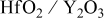 targets. Compositional, chemical, and electrical properties have been studied using X-ray photoelectron spectroscopy, X-ray diffraction, capacitance-voltage
 , and current-voltage measurements. O1s spectra shows a minimum defect due to M (Hf or Y)-OH and the bandgap was found
 . The measured
 and hysteresis in high frequency
 characteristics are used to study the pre-existing traps in the dielectric. Trapping kinetics as a function of stress time of
 have been investigated under low field
 from
 and
 .
Access this article
The computer you are using is not registered by an institution with a subscription to this article. Please choose one of the options below.
Purchase from
Purchase this article from our trusted document delivery partners.

Make a recommendation
To gain access to this content, please complete the Recommendation Form and we will follow up with your librarian or Institution on your behalf.
For corporate researchers we can also follow up directly with your R&D manager, or the information management contact at your company. Institutional subscribers have access to the current volume, plus a 10-year back file (where available).