
Abstract
A novel method for fabricating high efficiency metal  Schottky barrier solar cells is reported. The method is based on the fabrication of
 or
 thin films chemically deposited with and without silicotungstic acid (STA). The performances of the Schottky junctions fabricated with the films deposited with STA,
 , or
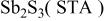 , are significantly higher than those deposited without STA. Under AM1 illumination, the photovoltaic properties of the improved
 diode showed
 ,
 ,
 , and efficiency
 . Analogous results are obtained on
 , where the photovoltaic response of the improved diode showed
 ,
 ,
 , and
 . The ideality factor
 and saturation current density
 were also significantly improved. C‐V measurements at 1 MHz showed that the barrier height
 of the fabricated diodes are 0.62 and 0.59 eV for
 and
 junctions, respectively, and 0.81 and 0.80 eV for
 and
 junctions, respectively. It is also observed that the
 values are independent of the metal work functions
 . This is attributed to the Fermi level pinning of
 or
 films deposited with and without STA.
Access this article
The computer you are using is not registered by an institution with a subscription to this article. Please choose one of the options below.
Purchase from
Purchase this article from our trusted document delivery partners.

Make a recommendation
To gain access to this content, please complete the Recommendation Form and we will follow up with your librarian or Institution on your behalf.
For corporate researchers we can also follow up directly with your R&D manager, or the information management contact at your company. Institutional subscribers have access to the current volume, plus a 10-year back file (where available).
