
Abstract
A buried  layer under a thin monocrystalline Si film has been successfully fabricated using wafer bonding and hydrogen‐induced delamination techniques. A Co and Si deposited wafer was brought into contact with a hydrogen‐implanted wafer at room temperature. During annealing in
 ambient, the hydrogen‐implanted wafer was split at the projected range of the implanted proton, remaining a thin monocrystalline Si layer bonded to the other wafer, and the buried
 layer was also formed through solid‐phase reaction. The electrical properties of the
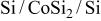 structure after different rapid thermal anneal treatments were studied by spreading resistance probe and current‐voltage measurements. © 1999 The Electrochemical Society. All rights reserved.
Access this article
The computer you are using is not registered by an institution with a subscription to this article. Please choose one of the options below.
Purchase from
Purchase this article from our trusted document delivery partners.

Make a recommendation
To gain access to this content, please complete the Recommendation Form and we will follow up with your librarian or Institution on your behalf.
For corporate researchers we can also follow up directly with your R&D manager, or the information management contact at your company. Institutional subscribers have access to the current volume, plus a 10-year back file (where available).
