
Abstract
Multi-level programmable photonic integrated circuits (PICs) and optical metasurfaces have gained widespread attention in many fields, such as neuromorphic photonics, optical communications, and quantum information. In this paper, we propose pixelated programmable Si3N4 PICs with record-high 20-level intermediate states at 785 nm wavelength. Such flexibility in phase or amplitude modulation is achieved by a programmable Sb2S3 matrix, the footprint of whose elements can be as small as 1.2 μm, limited only by the optical diffraction limit of an in-house developed pulsed laser writing system. We believe our work lays the foundation for laser-writing ultra-high-level (20 levels and even more) programmable photonic systems and metasurfaces based on phase change materials, which could catalyze diverse applications such as programmable neuromorphic photonics, biosensing, optical computing, photonic quantum computing, and reconfigurable metasurfaces.
Highlights
Pixelated non-volatile programmable photonic integrated circuits are proposed.
A record-high 20-level intermediate state of Sb2S3 with a minimal 1.2 μm spot size is realized using an in-house developed multi-level pulsed-laser writing system.
Pixelated programmable multi-level Mach–Zehnder interferometer and multimode interferometer based on Sb2S3 matrix are realized.
Very large-scale photonic linear processors based on pixelated Mach–Zehnder interferometer mesh are realized in simulation.
Export citation and abstract BibTeX RIS

Original content from this work may be used under the terms of the Creative Commons Attribution 4.0 license. Any further distribution of this work must maintain attribution to the author(s) and the title of the work, journal citation and DOI.
1. Introduction
Photonic integrated circuits (PICs), particularly those based on silicon photonics, have emerged as powerful platforms in a variety of fields, such as optical communications [1], sensors [2, 3], photonic neural networks [4–7], and quantum computing [8]. Programmable photonic devices, as one of the key components in PICs, perform linear and non-linear optical operations through optical manipulation technologies [9–12]. In silicon photonic platforms, the thermo-optical effect and plasma dispersion effect are commonly used to change the refraction index of silicon for optical phase shifts. However, these phase modulation approaches offer only small changes in the refractive index and require large photonic device footprints [13]. Moreover, microheater-induced thermal crosstalk and free-carrier-induced optical absorption impede the development of large-scale PICs.
Due to the large refractive index contrast ( ) between the amorphous and crystalline states of chalcogenide phase change materials (PCMs), PCMs have been used as a kind of reconfigurable material in rewritable compact discs [14]. Recently, researchers have investigated PCMs in nanophotonic platforms to perform programmable optical functions, including optical memories [15, 16], reconfigurable metasurfaces [17, 18], photonic switches [19], and neuromorphic photonics [20, 21]. Compared to traditional optical modulators, a significant advantage of PCMs is that they can maintain the phase state without additional energy, i.e. non-volatile. In addition, PCMs have prominent advantages such as large refractive index contrasts between different states, rapid and reversible switching between amorphous and crystalline states, excellent stability at room temperature, and high reproducibility (up to 1012) [22]. Germanium-antimony-telluride (GST) is the most widely used PCM in nanophotonics due to its high refractive index contrast and outstanding stability [23]. However, the phase transition of GST from the amorphous to the crystalline state causes an increase in both the real and imaginary parts of the refractive index. Crystalline GST with a high extinction coefficient results in a heavy absorption of light in the visible and near-infrared regimes, which makes GST a suitable material for performing optical intensity modulation in intensity-coded photonic systems [24, 25]. However, low-loss optical phase modulators are required for programmable photonic circuits, particularly Mach–Zehnder interferometer (MZI)-based architectures. Moreover, the optical loss induced by GST destroys the unitary properties of MZI meshes [26, 27]. Recently, wide-bandgap PCMs, such as GSST, Sb2S3, and Sb2Se3, have been investigated to reduce the optical loss in photonic interferometers and micro-ring resonators [28–36]. While there has been significant research development on low-loss PCMs in the amorphous and crystalline states, the study of the multi-level intermediate states at the micron scale is still in its infancy [37]. The research on programmable PCM-based PICs and metasurfaces primarily utilized thermal annealing and electrothermal switching [38–41]. As a result, programmable PICs and metasurfaces with ultra-high flexibility in phase modulation using multi-level PCMs with free-space laser switching were rarely reported, to the best of our knowledge.
In this paper, we propose a pixelated programmable Si3N4 photonic circuit with record-high 20-level intermediate states at 785 nm wavelength. Such a high degree of freedom in phase or amplitude modulation is achieved by a programmable Sb2S3 matrix, the footprint of whose elements can be as small as 1.2 μm, limited only by the optical diffraction limit. Moreover, we demonstrated the partial crystalline induced by the multiple laser pulse strategy is more stable and has a finer phase transition than the single-pulse strategy by using an in-house developed multi-level pulsed laser writing system alongside a portfolio of optical nanometrology technologies (see more details in the supplementary materials). We have shown the potential for improving the number of intermediate states of a single Sb2S3 element by precisely optimizing the power and number of pulses. By utilizing multi-level intermediate states achieved by our in-house developed micron-scale laser writing system, we simulated an Sb2S3-based phase shifter in a programmable MZI and demonstrated that it could achieve 30-level phase shift accuracy of π at 785 nm wavelength. In addition, we simulated the programmable 1 × 2 switch by precisely adjusting the level of crystallization of the Sb2S3 pixels on a multimode interferometer (MMI). In this way, we have demonstrated the availability of very large-scale pixelated non-volatile programmable PICs by simulation. We believe this work lays the foundation for laser-writing multi-level PICs and metasurfaces based on low-loss PCMs, and, therefore, opens up its potential applications in neuromorphic photonics, optical computing, photonic quantum computing, and reconfigurable metasurfaces.
2. Pixelated non-volatile programmable PICs
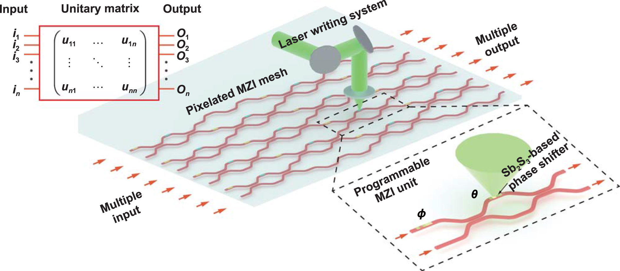
The proposed pixelated non-volatile programmable PICs are shown in figure 1. The architecture of the programmable photonic circuits consists of cascaded MZIs to perform matrix–vector multiplication (MVM), which is the main mathematical operation in artificial neural networks [4]. The unitary transformation matrix U(n) can be decomposed into the product of multiple unitary matrix U(2), and each unitary matrix U(2) is achieved by the basic programmable MZI unit. Each programmable MZI unit contains two 50:50 beam splitters and two Sb2S3-based pixelated phase shifters (outer phase shifter φ and inner phase shifter θ). The basic unitary matrix U(2) of each MZI unit is given by
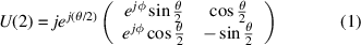

Figure 1. Pixelated programmable non-volatile photonic integrated circuits. The pixelated MZI mesh performs unitary transformation from input to output.
Download figure:
Standard image High-resolution imageThe low-loss Sb2S3 materials are deposited on the waveguides to act as phase shifters. By precisely controlling the power and number of the laser pulses, the focused laser beam is used to realize multi-level intermediate states of Sb2S3 pixels with a length of 1 μm. The multi-level intermediate states of Sb2S3 pixels with different refractive indices can realize multi-level phase shifts with almost no energy loss. The movable laser writing system (with more details regarding figure 3 and the supplementary material) is used to switch multiple Sb2S3 pixels, as shown in figure 1. By combining multi-level intermediate states with micron-scale laser writing, 30-level/π phase shift accuracy can be achieved, which meets the requirements of artificial neural networks. In addition, compared to GST materials with large absorption loss, low-loss Sb2S3-based phase shifters have the potential to be applied in very large-scale PICs (up to 100 × 100).
3. Results and discussion
3.1. Optical characterization of Sb2S3 material
In order to apply Sb2S3 in the field of pixelated programmable PICs, it is essential to determine the refractive index (real part n and imaginary part k) of amorphous Sb2S3 (aSbS) and crystalline Sb2S3 (cSbS) and the crystallization temperature. A 10 nm-thick Sb2S3 film was deposited by radio frequency (RF) sputtering on a standard 500 μm-thick silicon substrate. After that, a 20 nm-thick SiO2 film, which acts as the protective layer, was deposited by PECVD at 100 °C to prevent sulfur loss during the phase transition process. The schematic diagram of the multi-layer sample is shown in figure 2(a). The deposited Sb2S3 material at the very beginning was in the amorphous state. To crystallize the Sb2S3 film and determine the crystallization temperature, four Sb2S3 samples were annealed at different temperatures (starting from 240 °C to 360 °C with an increment of 40 °C) for 5 min. As shown in figure 2(b), the film surface shows a non-uniform pattern when the heating temperature reaches up to 320 °C, which is due to the nucleation and growth of crystals. The optical constants of the originally deposited Sb2S3 sample and four Sb2S3 samples heated at different temperatures are measured by a spectroscopic ellipsometer, as illustrated in figure 2(c). More details on the ellipsometer can be found in the supplementary material. As expected from the Sb2S3 micrographs, the Sb2S3 starts to crystallize at 320 °C, after which the refractive index changes dramatically. According to the measurement results, the fitted bandgaps of cSbS and aSbS are 1.53 eV and 2.04 eV, respectively. The bandgaps of amorphous and crystalline Sb2S3 are much larger than those of GST, which means that Sb2S3 could significantly reduce optical loss compared to GST in the visible and near-IR wavebands [36]. As shown in figure 2(d), the refractive indexes of aSbS and cSbS were compared with other measurement results from [35]. The slight difference may be caused by the material roughness, the fabrication process, or the measurement error.

Figure 2. Optical characterization of Sb2S3 material. (a) The schematic diagram of the Sb2S3 sample. (b) Optical microscope images of the Sb2S3 samples heated at different temperatures. The scale bar is 50 μm. (c) The refractive indexes of five Sb2S3 samples heated at different temperatures, which were measured by a spectroscopic ellipsometer. (d) The reconstructed optical constants are compared with those in [35].
Download figure:
Standard image High-resolution image3.2. Laser-writing multi-level intermediate states of Sb2S3 elements
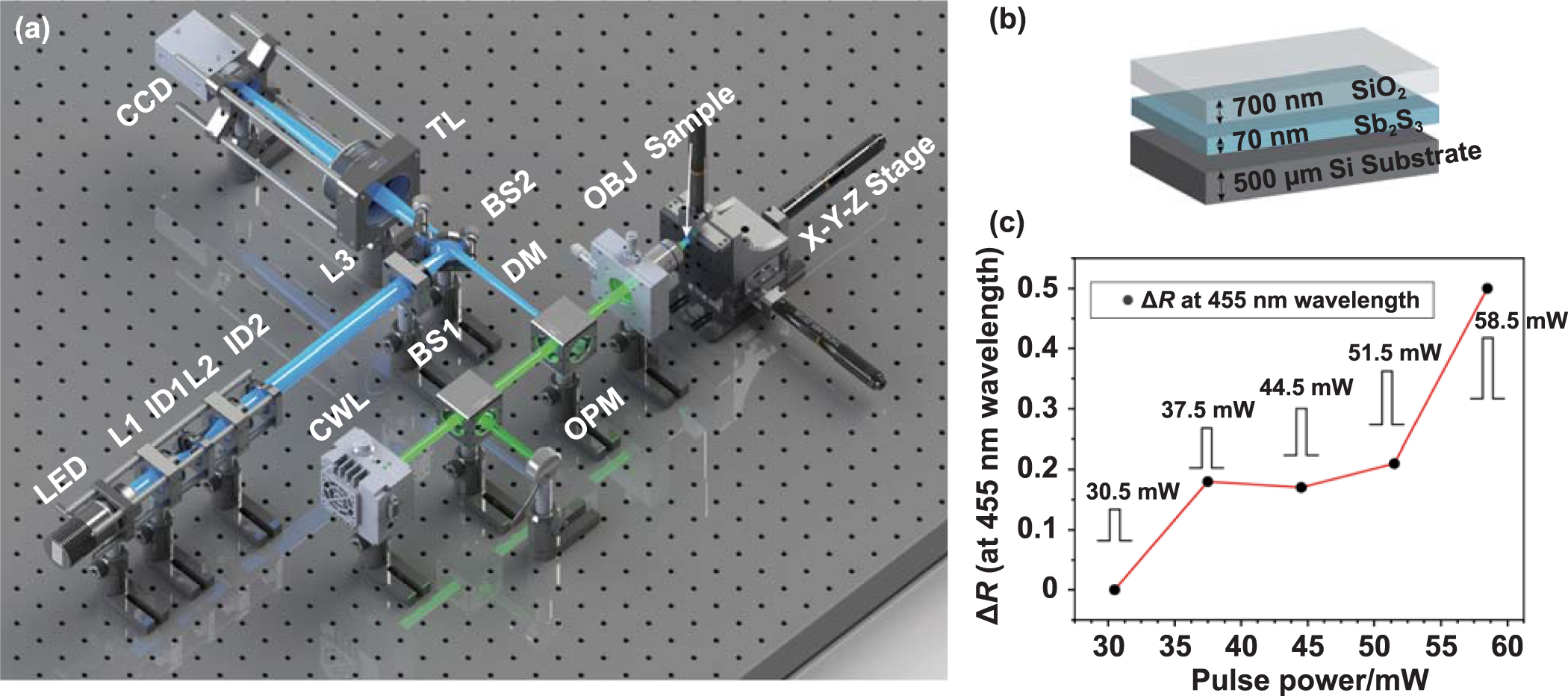
A programmable multi-level Sb2S3 matrix consists of a large number of Sb2S3 elements. The fine phase transition and the footprint of a single Sb2S3 element are crucial for the performance of the programmable PICs and metasurfaces. In this section, we investigate the laser-writing multi-level intermediate states of a single Sb2S3 element at the microscale. A 70 nm-thick Sb2S3 film was deposited on the silicon substrate, after which a 700 nm-thick SiO2 was deposited as the protective layer. The experimental setup of the in-house developed pulsed laser writing system for the multi-level phase transition of Sb2S3 matrix can be found in figures 3(a) and S1: a high-power laser beam generated by a continuous wave laser (CWL) at 520 nm wavelength is focused by a 50×/0.6NA objective lens on single Sb2S3 elements to perform phase transition. The full width at half maximum (FWHM) of the focused laser spot size is 1.2 μm. According to the transfer matrix method, the degree of crystallization of Sb2S3 elements can be characterized by the reflectance of the phase-change region [42, 43]. An optical brightfield microscope was then added to the laser-writing setup in order to navigate the region of interest and measure the reflectance of phase-transition regions in-situ. The illumination and imaging light paths are shown in blue in figure 3(a). The central wavelength and the bandwidth (FWHM) of the LED are 455 nm and 18 nm, respectively. The power of the LED is too low to impact the phase transition. More details about the experimental setup can be found in supplementary materials.

Figure 3. The pulsed laser writing system and the measured reflectance that reflects the multi-level intermediate states of Sb2S3 elements. (a) The experimental setup of the pulsed laser writing system. L, lens; ID, iris diaphragm; CWL: continuous wave lasers; BS, beam splitter; OPM, optical power meter; DM, dichroic mirror; OBJ, objective lens; TL, tube lens. (b) The schematic diagram of the Sb2S3 sample. (c) The measured reflectance that reflects the different intermediate states of Sb2S3 elements at different laser powers (from 30.5 mW to 58.5 mW).
Download figure:
Standard image High-resolution imageSingle laser pulses with different powers were used to induce different degrees of crystallization of Sb2S3 elements. The laser power generated by the laser diode changes from 30.5 mW to 58.5 mW, and the laser pulse duration is 10 ms. The reflectance difference ( ) is used to determine the crystallize fraction given by
where R is the measured reflectance of intermediate states of Sb2S3 elements, and Ra is the reflectance of aSbS. The ΔR of the phase-change regions at different laser powers was measured and shown in figure 3(c). When the laser power is too low (less than 30.5 mW) to reach the crystallization temperature, there is no change in the reflectance of the Sb2S3, and the Sb2S3 pixel remains in the amorphous state. As the laser power increases from 37.5 mW to 51.5 mW with a step of 7 mW, the aSbS starts to partially crystallize and the reflectance increases before reaching up to the peak reflectance (i.e. the point where full crystallization happens). A slight variation in the reflectance of intermediate states of Sb2S3 can be observed when the laser power is increased from 37.5 mW to 51.5 mW. The underlying physics of why ΔR remains the same at pulse power ranging from 37.5 mW to 51.5 mW, unfortunately, is unknown as of now, but it again demonstrates the fact that the relationship between laser power and the reflectance difference is nonlinear [44]. Hence, we would like to leave this as an open question for future study and discussion, while focusing on the demonstration of the multi-level intermediate states of Sb2S3 alongside its potential applications in this paper. As we increase the pulse power from 51.5 mW to 58.5 mW, we observe a further increase in the reflectance difference, which indicates the generation of more intermediate states. In addition, the central damage of phase-change regions affects the stability of crystallization [32, 36]. Due to the low absorption of aSbS and the burn-in-effect, local damage and defects can be induced by the high-power and long-period laser pulse illumination in the phase-change regions. The central damage images of Sb2S3 elements after high laser power excitation are shown in figure S2. As a result, the crystallization stability of Sb2S3 induced by a single high-power and long-duration laser pulse limits the applications of multi-level intermediate states.
To improve the crystallization stability, we use different numbers of low-power laser pulses to crystallize aSbS pixels (from 0 to 350 pulses). The power of the laser beam is 28.4 mW, and the pulse period and duty cycle of the square pulses are 80 ms and 50%, respectively. The reflectance of the Sb2S3 induced by different numbers of pulses was measured, as shown in figure 4(a). The microscopic images of the phase-transition pixel under different numbers of pulses (0, 160, 240, 350) are shown in figure 4(b). The microscopic images of 20-level intermediate states are illustrated in figure S3. When the number of pulses is less than 120, the reflectance remains constant because the temperature of the laser heating area does not reach the crystalline temperature (around 320 °C). As the number of pulses exceeds 120, the reflectance gradually increases. The increase in reflectance is linearly related to the number of pulses. The reflectance difference reaches its peak value of 0.58 after 320 laser pulses. In comparison, the reflectance difference of cSbS heated on a heating panel is 0.60, which is slightly higher than that of cSbS pixels induced by the focused laser. This indicates that the reflectance difference between Sb2S3 induced by thermal annealing and the focused laser demonstrates the complete crystallization after 320 laser pulses. The gradual increase in reflectance and absence of darker points in the phase-change region exclude the influence of local damage induced by high-power laser pulses. In addition, we performed the measurement of Raman spectrum to demonstrate the cSbS induced by laser pulses, as shown in figure 4(c). The Sb2S3 processed by thermal annealing and laser heating has the same set of peak wavelengths corresponding to known vibration modes that affirm crystallization [32]. The experimental results demonstrate the efficiency of the laser heating process in the crystallization of PCMs. The 20-level intermediate states of single Sb2S3 pixels were realized in the range of 120–320 pulses. The diameter of the phase-transition pixels is about 1.2 μm, which is caused by the focused laser. Compared with the single-pulse crystallization strategy, the partial crystallization strategy using low-power, multi-pulse lasers is much more stable. The longer period and pulse interval allow for a longer duration of heat transfer from the center to the edge in the phase-transition region, alleviating the issue of excessive temperature in the center of the phase-transition region. Therefore, the multiple low-power pulse crystallization approach is more suitable for achieving multi-level intermediate states. Moreover, the multi-pulse crystallization approach has also been demonstrated to greatly improve cycling durability [34]. We set 10 pulses as the crystallization step to guarantee the distinct reflectance difference of 20-level intermediate states and improve the stability of crystallization. The slope of  with the number of pulses could go down with a proper reduction in optical power. The more intermediate states of Sb2S3 pixels could be realized by optimizing the pulse power and pulse duration. In addition, more precise measuring instruments are required to distinguish the minor reflectance differences of different intermediate states of Sb2S3 pixels. While the main focus of this paper is the crystallization of Sb2S3, it is worth noting that multi-level intermediate states during the amorphization process can also be realized in a similar way [34, 44]. Compared to the crystallization process, the amorphization process requires higher temperature and shorter laser pulse width (from femtoseconds to nanoseconds). The parameters of laser pulses, including the laser power, the pulse width and the repetition frequency, need to be optimized through experiments to realize multi-level intermediate states. In terms of cyclability, there were some studies discussing the cycling duration of PCMs, especially Sb2S3 [34, 36]. Delaney et al [36] demonstrated a fast degradation of Sb2S3 after around 1000 switching cycles. To improve the cycling durability, [34] demonstrated a multi-pulse irradiation-based method to obtain greater cycling durability. It is worth noting that the region irradiated by laser pulses tends to form irreversible deformation due to local melting and surface tension, while lowering pulse energy reduces the deformation and thus improves cycling durability. Compared with a single pulse with high energy, the method of using multiple pulses with lower pulse power tends to improve the cycling durability.

Figure 4. Multi-level intermediate states of Sb2S3 induced by different numbers of laser pulses. (a) The ΔR of intermediate states of Sb2S3 elements induced by different numbers of laser pulses (from 0 to 350 pulses). (b) The optical microscope images of the phase-transition pixels under different numbers of pulses (0, 160, 240, 350). The Sb2S3 pixel without laser pulse illumination is in the amorphous state; the aSbS pixels after the illumination by the number of pulses in 160 and 240 are in the intermediate states; the aSbS elements excited by 350 pulses are in the fully crystalline state. The scale bar is 5 μm. (c) Raman spectra of aSbS and cSbS induced by thermal annealing and the focused laser.
Download figure:
Standard image High-resolution image3.3. Pixelated non-volatile programmable Si3N4 photonic circuits
The programmable integrated photonic circuits based on programmable MZIs have been proposed to perform various linear functions, such as MVM, which behaves similarly to the field programmable gate arrays in electronic integrated circuits [45]. The MZIs, as basic building blocks, consist of thermal phase shifters with a large footprint, which impede very large-scale integration of PICs. In this section, we propose pixelated non-volatile programmable PICs based on the multi-level intermediate states of Sb2S3 pixels, as shown in figure 5(a). The low-loss Sb2S3 is first deposited on the multimode interferometer (MMI) and waveguide, after which a movable laser spot is focused on the different Sb2S3 pixels to induce partial crystallization. The Sb2S3 pixels are then switched to intermediate states to affect light propagation. In this paper, we simulated two fundamental pixelated programmable photonic integrated devices, i.e. programmable MZI and MMI, to demonstrate the feasibility of the programmable Sb2S3 matrix in PICs, as shown in figures 5(b) and (c). The multi-level intermediate states of Sb2S3 used in the simulation are determined by our experimentally characterized Sb2S3 thin film. The cross-section of the sample is shown in figure 6(a), which is consistent with the structure used in simulation. The thickness of Sb2S3 film is 10 nm, which was determined through simulation optimization. Additionally, a 200 nm-thick Si3N4 film was prepared for waveguides. Five-level intermediate states of 10 nm-thick Sb2S3 pixels were realized experimentally; see the micro images in figure 6(b). The diameter of phase-transition pixels is 1 μm, which corresponds to the spot size of the focused laser. Based on the reflectance of the Sb2S3 pixels at intermediate states, the crystalline fraction can be determined, and the effective permittivity ( ) and the refractive index of intermediate Sb2S3 pixels can be calculated according to the effective medium theory [46] (see more details in the supplementary materials).
Figure 5. Pixelated non-volatile programmable photonic integrated circuits. (a) The schematic diagram of the pixelated non-volatile programmable photonic integrated circuits based on multi-level intermediate states. The inset denotes the cross-section of the waveguide. (b) The programmable MZI, in which Sb2S3 pixels are used to modulate the optical phase. (c) The programmable 1 × 2 optical switch based on Sb2S3 matrix.
Download figure:
Standard image High-resolution image
Figure 6. 5-level intermediate states of 10 nm-thick Sb2S3 pixels. (a) The cross-section of the 10 nm-thick Sb2S3 layer on the Si3N4 layer. (b) The ΔR of Sb2S3 pixels as a function of intermediate states.
Download figure:
Standard image High-resolution imageFirstly, we simulated the symmetrical MZI at 785 nm wavelength. A Sb2S3 film was assumed to be deposited on two arms of the MZI to modulate the optical phase without damaging the unitary properties. The width and height of the Si3N4 waveguide are 500 nm and 200 nm respectively, to determine the single-mode condition. Because the thickness of the Sb2S3 film affects the optical mode in the waveguides and therefore, the phase modulation and the optical loss, we simulated Sb2S3 films of different thicknesses (from 10 nm to 30 nm) on the waveguides to determine the appropriate thickness of the Sb2S3 layer for phase modulation. The figure of merit (FOM)  was used to estimate the loss of the cSbS phase shifters, and
  is the length of the Sb2S3 patch to realize the π phase shift in each waveguide arm. The simulated results are shown in figure 7(b). Apparently, a thinner Sb2S3 film with a larger
  corresponds to a higher FOM. In addition, the mode overlaps between bare waveguides and waveguides covered with Sb2S3 are higher for thinner Sb2S3 films. The simulated results of mode overlaps are shown in figure S5. This means that the 10 nm-thick Sb2S3 film has a lower optical insertion loss. Thus, a 10 nm-thick Sb2S3 matrix was applied in the MZIs, and the simulation electric field intensity profile can be seen in figure 7(a). By combining the 5-level intermediate states and the number of laser-writing Sb2S3 pixels, we simulated the 30-level transmission of bar and cross output (Eo
1 and Eo
2), as shown in figure 7(c). It is worth noting that the simulated MZI can return to the initial state by inducing Sb2S3 pixels to the initial amorphous state [29].
corresponds to a higher FOM. In addition, the mode overlaps between bare waveguides and waveguides covered with Sb2S3 are higher for thinner Sb2S3 films. The simulated results of mode overlaps are shown in figure S5. This means that the 10 nm-thick Sb2S3 film has a lower optical insertion loss. Thus, a 10 nm-thick Sb2S3 matrix was applied in the MZIs, and the simulation electric field intensity profile can be seen in figure 7(a). By combining the 5-level intermediate states and the number of laser-writing Sb2S3 pixels, we simulated the 30-level transmission of bar and cross output (Eo
1 and Eo
2), as shown in figure 7(c). It is worth noting that the simulated MZI can return to the initial state by inducing Sb2S3 pixels to the initial amorphous state [29].
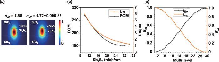
Figure 7. The programmable MZI based on multi-level intermediate states of Sb2S3 pixels. (a) The normalized intensity distribution of waveguide mode for aSbS (left) and cSbS (right). (b) The FOM and Lπ of different thicknesses of Sb2S3 films. (c) The simulated transmission of bar (Eo 1) and cross (Eo 2) outputs of the MZI.
Download figure:
Standard image High-resolution imageIn addition, we studied the programmable Si3N4 MMI based on the Sb2S3 matrix to perform a 1 × 2 switch at a 785 nm wavelength in simulation. As shown in figure 8, the width and length of Sb2S3 matrix are 4 μm and 17 μm, respectively. The size of a reconfigurable Sb2S3 pixel is 1 × 1 μm, and the thickness of Sb2S3 film remains the same as before (i.e. 10 nm). The total number of pixels is 68 (4 × 17). The Sb2S3 pixels are in the initial amorphous state, and the MMI performs a 50:50 power split, as shown in figures 8(a) and (b). To switch the optical power to the lower waveguide, we optimize the intermediate states of the Sb2S3 matrix in the MMI region based on a multiple-value search algorithm. Each Sb2S3 pixel has six intermediate states, which correspond to six refractive index values, i.e. 2.75 (aSbS),  (iSbS1),
  (iSbS2),
  (iSbS3),
  (iSbS4),
  (cSbS), which have been experimentally determined in the previous section. Similar to the direct-binary-search algorithm, we provide a random pattern as the initial guess. The state of one Sb2S3 pixel is switched, and the FOM is simulated in one simulation. The state of the pixel is retained if the FOM is improved; otherwise, the pixel is brought back to its previous state. In this way, all 68 pixels with 6 values are simulated in one iteration. When the FOM stops improving after several iterations, we can ensure that the best results are obtained. As shown in figures 8(c) and (d), 84.50% transmission of the lower waveguide is obtained. For comparison, we also optimized the same Sb2S3 matrix size but with only two states for each pixel, i.e. aSbS and cSbS. The simulated results along with the pattern of the Sb2S3 matrix are shown in figures 8(d) and (f). The transmission (77.47%) of the binary Sb2S3 matrix configuration is apparently lower than that of the multi-level Sb2S3 matrix. The simulated results of the programmable MMI demonstrate the superior performance achieved with the multi-level Sb2S3 compared to binary Sb2S3. Moreover, the multi-level Sb2S3 induced by the focused laser pulses has more potential applications in programmable PICs and metasurfaces than the Sb2S3 with only binary states. As an example, we proposed and simulated a single-layer continuous varifocal metalens based on multi-level Sb2S3 pixels. More details of the metalens can be found in the supplementary materials.
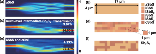
Figure 8. Optically programmable MMI based on multi-level Sb2S3 matrix. The normalized intensity distribution shown in (a), (c) and(e) correspond to (b) the uniform aSbS, (d) the programmed multi-level Sb2S3 matrix, and (f) the programmed binary Sb2S3 matrix, respectively. The simulation was implemented by the 3D eigenmode expansion method.
Download figure:
Standard image High-resolution image3.4. Pixelated programmable MZI-based photonic linear processor
To validate the proposed pixelated PICs, an MZI-based photonic linear processor that uses Sb2S3-based pixelated phase shifters is realized by simulation, as shown in figure 9. The structure of the photonic linear processor is shown in figure 1, and the Sb2S3-based phase shifters with 30-level/π accuracy are used in the photonic linear processor. The photonic linear processor is used to perform convolution between kernels and an image, as shown in figure 9(a). The photonic system with nine inputs can perform simultaneous convolution on an image with nine 3 × 3 kernels. Each 3 × 3 kernel filter is flattened into a 1 × 9 row vector, and the resulting nine kernel vectors form the 9 × 9 kernel matrix M. Then the kernel matrix M is decomposed as  based on singular value decomposition. U and
  are unitary matrices, which can be decomposed into multiple cascaded MZIs using the Clements' scheme [47], and the diagonal matrix Σ is implemented by a column of MZIs. The raw image is divided into multiple 3 × 3 patches, and then flattened into column vectors as inputs. The input signals propagate through the Sb2S3-based kernel matrix to realize MVM and convolution. The nine outputs from o1 to o9 correspond to nine kernel filters, and the sequence of outputs is reshaped into processed images. The raw image and processed images are shown in figure 9(a). The whole pixelated kernel matrix and Sb2S3-based phase shift values are shown in figure S7.

Figure 9. The pixelated programmable MZI-based photonic linear processor. (a) The schematic of the pixelated photonic linear processor. (b) The element values of the unitary matrix (U(16) and U(64)), the recovered matrices (UP(16) and UP(64)) and the error matrices (Ud(16) and Ud(64)). (c) The fidelity of the pixelated matrix.
Download figure:
Standard image High-resolution image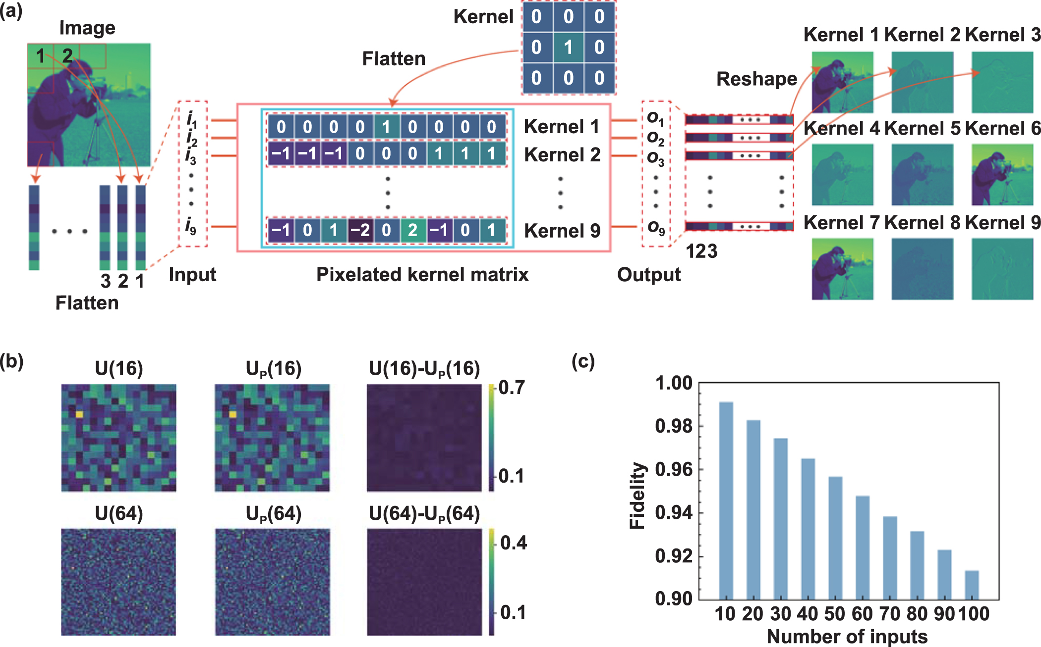
To validate the accuracy of pixelated kernel matrix in very large-scale PICs, we generated random unitary matrices U(16) and U(64). The unitary matrices are decomposed into cascaded MZIs, and the phase shifters are discretized into multi-level phase values. The inner phase shifts θ (range from 0 to π) are discretized to 30-level phase values, and the outer phase shifters φ (range from −π to π) are discretized into 60-level phase values. Then the discrete matrices (UP(16) and UP(64)) and the error matrices are shown in figure 9(b). Moreover, a standard measure of fidelity is used to quantify the performance of the pixelated matrix. The fidelity is given by
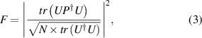
where N is the number of inputs. The simulated fidelity of pixelated matrices is shown in figure 9(c). The fidelity of the very large-scale MZI mesh (100 × 100) is maintained at above 90%. Overall, the simulation results indicate that the pixelated programmable MZI-based photonic linear processor has the potential to be scaled up to a large size.
4. Conclusion
In this work, we proposed and demonstrated the pixelated programmable Si3N4 photonic circuits with record-high 20-level intermediate states at 785 nm wavelength by utilizing a programmable Sb2S3 matrix. The 20-level intermediate states of each programmable Sb2S3 element have a minimal 1.2 μm footprint, limited only by the optical diffraction limit of the in-house developed multi-pulse laser-writing system. Moreover, we have shown the potential of further improving the number of intermediate states of a single Sb2S3 element by precisely optimizing the power and number of pulses. We believe the Sb2S3-matrix-based programmable PICs could have a positive impact on general-purpose programmable photonic circuits and photonic neural networks. Moreover, we hope our work could open up the applications of laser-induced programmable devices for neuromorphic photonics, optical computing, photonic quantum computing, and reconfigurable metasurfaces.
5. Fabrication
5.1. Fabrication of Sb2S3 samples
Sb2S3 thin films were deposited on the silicon substrates (N-type, 100) under vacuum by RF magnetron sputtering using an Sb2S3 target. Ar gas was introduced into the chamber at a flow rate of 20 sccm, and the magnetron sputtering power was 20 W. The deposited speed was 1.37 nm·min−1, which was measured by an optical ellipsometer. Then, a SiO2 cladding layer was deposited by PECVD at 100 °C, which is lower than the crystalline temperature of Sb2S3.
5.2. Suggested fabrication method for pixelated PICs
The proposed pixelated PICs can be fabricated based on the existing silicon photonics fabrication technology. The suggested fabrication process can be detailed as follows.
A 200 nm-thick Si3N4 film is deposited on SiO2 (2 μm) on the silicon substrates by PECVD process, after which the photonic circuits can be fabricated using three-step deep ultraviolet lithography or electron-beam lithography process. The first lithography step is prepared for fabricating alignment markers. The resist that is spin-coated on the wafer is selectively exposed for making the alignment markers. Then the resist is developed using specific solvents. The gold and chromium are evaporated over the whole wafer by electron-beam evaporation. The sacrificial layer (unexposed resist) is washed away in acetone, and the gold on the sacrificial layer is lifted off together with the sacrificial layer. Then, the gold in direct contact with the substrate remains and is formed into alignment markers. The second lithography step is used to fabricate the Si3N4 waveguides. The lithography process is similar to the first lithography step. The distinct steps involve replacing the lift-off process with an etching process. The Si3N4 film is etched by the inductively coupled plasma etching. Then the resist is removed in acetone. The third lithography process is used to fabricate the Sb2S3 pixels. The fabrication process is similar to the first step. The Sb2S3 material is deposited by RF magnetron sputtering (in the section 5.1). Finally, the chip is cladded by the SiO2 as a protective layer via low-temperature PECVD.
After fabricating PICs, the pulsed laser writing system can be used to create pixelated non-volatile programmable PICs, see more details in section 3.2. By controlling the position of the laser beam with the objective lens and the sample stage, a programmable Sb2S3 matrix can be achieved. The resolution of the laser writing system is only limited by the optical diffractive limit. The laser power and the number of laser pulses are controlled to induce multi-level intermediate states of the Sb2S3 pixels. The states and phase values of the Sb2S3 pixels are determined by the calibration experiments, as detailed in sections 2 and 3.
Acknowledgments
This work was funded by the National Nature Science Foundation of China (Grant Nos. 52175509 and 52130504), National Key Research and Development Program of China (2017YFF0204705), 2021 Postdoctoral Innovation Research Plan of Hubei Province (0106100226). Thanks engineers Guangxue Zhang and Pan Li in Optoelectronic Micro&Nano Fabrication and Characterizing Facility, Wuhan National Laboratory for Optoelectronics of Huazhong University of Science and Technology for the support in device fabrication (RF magnetron sputtering and PECVD).
Supplementary data (1.0 MB PDF)