
Abstract
Organic electrochemical transistors (OECTs) exhibit significant potential for applications in healthcare and human-machine interfaces, due to their tunable synthesis, facile deposition, and excellent biocompatibility. Expanding OECTs to the flexible devices will significantly facilitate stable contact with the skin and enable more possible bioelectronic applications. In this work, we summarize the device physics of flexible OECTs, aiming to offer a foundational understanding and guidelines for material selection and device architecture. Particular attention is paid to the advanced manufacturing approaches, including photolithography and printing techniques, which establish a robust foundation for the commercialization and large-scale fabrication. And abundantly demonstrated examples ranging from biosensors, artificial synapses/neurons, to bioinspired nervous systems are summarized to highlight the considerable prospects of smart healthcare. In the end, the challenges and opportunities are proposed for flexible OECTs. The purpose of this review is not only to elaborate on the basic design principles of flexible OECTs, but also to act as a roadmap for further exploration of wearable OECTs in advanced bio-applications.
Highlights
Principles of flexible OECT device design and material selection are demonstrated.
The manufacturing techniques and guidelines for developing flexible OECTs are outlined.
Overview of the bioelectronic applications and prospects of flexible OECTs are provided.
Export citation and abstract BibTeX RIS

Original content from this work may be used under the terms of the Creative Commons Attribution 4.0 license. Any further distribution of this work must maintain attribution to the author(s) and the title of the work, journal citation and DOI.
1. Introduction
Since the first appearance of organic electrochemical transistors (OECTs) in 1984 [1], OECTs have aroused enormous research attention and been explored from the operation mechanism [2–5], materials selection [6–13], novel device layout [5, 14–17], and various applications (such as biosensors [18–23], neuromorphic computing [24–30], digital logic circuit [14, 31–34] and tissue engineering [35–39]). Unlike conventional three-terminal thin-film transistors, the operation of organic electrochemical transistor (OECT) is dependent on mixed ionic-electronic interactions and coupled transport mechanisms, electrolyte ions permeate the active channel volumetrically and regulate the semiconductor's redox state [40], thus leading to a tunable channel current. This ion–electron coupling effects offer extraordinary advantages for OECTs, including high transconductance (up to the milliSiemens level in micron-scale devices), low operating voltage (below 0.5 V), and excellent biocompatibility [10] Thus, OECTs with micrometer-scale size possess high signal amplification capabilities, low power consumption, and compatibility with the surrounding biological environment, making them ideal for a variety of bioelectronic applications [41, 42], and it is noteworthy that the estimated market size for OECT-based biosensors is a substantial US$ 13 billion annually [43, 44].
Recently, reviews focusing on semiconductors design [6, 45, 46], fundamental device physics [10, 47], and bioelectronics applications have been conducted to summarize the rapid development of OECT [48]. Despite this, the studies in question have primarily dealt with inflexible OECTs, a feature that could introduce interface anomalies and trigger immune responses within biological tissues. To mitigate this concern, the incorporation of polymer semiconductors, characterized by low Young's modulus and straightforward device design, makes OECTs a highly promising candidate for flexible and stretchable electronics [49, 50]. Flexible OECTs have been developed for skin electronics, with research involving soft functional materials, biocompatible devices, and healthcare-related applications [51–53]. Undoubtedly, the particular interest of flexible OECTs is their skin-conformable and even implantable capabilities, which is expected to change the way humans interact with the world in the future [54–56]. A critical challenge in flexible OECTs is the design and optimization of soft functional materials [57, 58]. The superposition of requirements in electric and mechanical engineering makes the material structure complex. In general, multi-component composites and modification strategies are utilized to achieve compatible electrical and mechanical properties. However, cumbersome synthesis processes and expensive costs limit the development of material engineering [49]. As an alternative solution, manufacturing techniques could enhance flexibility via optimizing mechanical-structure design and dispersing stress, with greater feasibility for existing materials [35, 59–61]. However, few reviews have summarized and analyzed the characteristics of these advanced micro-nano manufacturing techniques. Moreover, as the social economy rapidly progresses, there is greater attention on life sciences and healthcare, with the purpose of elevating, substituting, and extending human bodily functionalities [18]. According to reported flexible OECT-based bioelectronics, biosensors for detecting physical, chemical and biological signals, artificial synapses for mimicking human learning and memory functions, and bioinspired nervous systems for sensing, transmitting and processing signals, have been developed. A review is urgently needed to summarize and analyze the research progress and roadmaps for the development of flexible OECT in diversified bioelectronic applications.
In this review, we offer a comprehensive overview of the latest developments in flexible OECTs, particularly focusing on corresponding advanced manufacturing techniques and demonstrated bioelectronics applications. Here, the application examples involve flexible (uniaxial deformation) and stretchable (out-of-plane bending) mechanical deformations, and no obvious distinction between flexibility and stretchability is made. The first two chapters elaborate on the working mechanism and flexible functional materials. The third part summarizes and analyzes the characterizations of commonly used fabrication technologies for flexible OECTS, including photolithography and screen/inkjet/transfer printing. And representative examples are given with detailed parameters presented. In the fourth part, we summarize advanced applications of flexible OECTs in the field of bioelectronics, which are mainly classified into three categories: physical/chemical/biosensors; artificial synapses/neurons; and bioinspired neuromorphic/nerve systems. In the end, we give an overall summarization and discussion on the challenges that lie ahead and future research directions of flexible OECTs. And figure 1 presents a systematic outline of this review.
Figure 1. Systematic outline of this review. A combination of soft materials (the foundation of flexible OECTs), optimized device structure design, and advanced manufacture techniques for functionalized OECTs and explored integrated neuromorphic system applications. In contrast, realistic scenario-oriented applications also make demands on material selection and device functionality. Such positive closed loops have facilitated the development of flexible electronics.
Download figure:
Standard image High-resolution image2. Device physics
2.1. Working mechanism
The operating mechanism of OECT relies heavily on the volumetric capacitance of organic semiconductors [3]. The electrolyte ions compensate for charges in the channel via applying gate voltage, thereby modulating the electrochemical doping state of the transistor channel. Specifically, when applying gate voltage, ions (anion or cation) are injected from the liquid or solid electrolytes into the organic semiconductor films. Therefore, the introduction of electronic charge from the source electrode balances the extra charges (holes or electrons), subsequently enhancing the charge density within the transistor channel and enabling control over the output current of p- or n-type OECTs. The redox state fitting with the channel conductivity, enables excellent transconductance values (up to milliSiemens) for micrometer-scale OECT devices [36]. As described in figure 2(a), fundamental device physics theory of OECT is based on the Bernards model [62], consisting of an electronic circuit and an ionic circuit. Ionic and electron circuits represent that ions movement through the gate-electrolyte-channel structure and electrons movement through the source-channel-drain structure, respectively. Specifically, the electronic circuit is considered to be an adjustable resistor, so that the local potential regulates the drift behavior of electrons. And the ionic circuit incorporates a series resistor–capacitor structure, allowing ions to flow in the electrolyte and be stored in the channel. Such a model well fits the experimental results of OECT, and a quantitative prediction of the transconductance (gm) that can be derived from the following formula [63]:


Figure 2. Schematic illustration of operating mechanism and different architectures of flexible OECTs. (a) Fundamental comprehensive about OECT device physics. (b) Transfer curves of depletion and accumulation modes of OECT. (c) Typical device structures for OECT, including top-gated OECT, side-gated OECT, vertical OECT, and fiber-based OECT.
Download figure:
Standard image High-resolution imagewhere d, L and W represent the thickness, length and width of channel. μ and C* represent the carrier mobility and the channel capacitance, influencing the ionic–electronic transport and coupling process. VG and Vth represent the gate voltage and threshold voltage, respectively. gm is the most important parameter of OECT and characterizes the signal amplification ability. Noteworthy, gm is associated with the channel thickness in OECT, while it is not in traditional field effect transistors [64].
Optimized gate electrodes facilitate the realization of highly efficient gating in OECT [11], because the potential distribution in the transistor channel relies on the intrinsic properties and geometry of the gate electrodes [65]. Employing polarizable electrodes (e.g. gold or platinum) as gates, two capacitors in the ionic circuit will be formed [3]. One of capacitor pertains to the electrical double layer established at the interface between the gate and electrolyte, while the second is associated with the volumetric capacitance of the semiconductor. However, the applied gate voltage drops significantly at the smaller capacitor of the series double capacitor, thus limiting the output performance [66]. To realize the efficient gating, enlarged geometry and modified surface for gate are feasible to maximize the capacitance at gate-electrolyte interface. For example, thick poly(3,4-ethylenedioxythiophene) polystyrene sulfonate (PEDOT: PSS) was directly deposited onto the Au gate to minimize the electrochemical impedance between the transistor channel and Au gate electrode [67]. Alternatively, non-polarizable Ag/AgCl electrode also enables minimizing the voltage drop for efficient gating at the gate-electrolyte interface.
According to the operating mode of OECT, it can be divided into depletion and accumulation modes, as illustrated in figure 2(b). In depletion mode, devices typically exhibit high current state without gate voltage, since channel polymer are highly conductive with an excess of free charge carriers [68]. PEDOT: PSS represents the most typical channel material operating in depletion mode, once gate biased with positive voltage, cations present in the electrolyte are injected into the semiconductor bulk and result in the compensation of the anions, thus the device is switched from ON to OFF state. In accumulation mode, OECT is switched from OFF to ON state when applying a gate. The drain currents increase with ions injecting and accumulating in the channel. Owing to the low power consumption, effort has been devoted to developing p-type and n-type redox active semiconductors operating in accumulation mode [69], which presenting a great application potential in low-power and wireless bioelectronics. Table 1 summarizes the key parameters of typical OECT devices (rigid and flexible) reported in recent five years, to provide a research benchmark for further high-performance flexible OECTs.
Table 1. Summary of key parameters of typical OECTs reported in recent five years.
| Channel materials | Flexibility | Electrolyte | Vth (V) | SS (mV dec−1) | gm (mS) | On/off ratio | References |
|---|---|---|---|---|---|---|---|
| PEDOT: PSS | ✘ | 0.1 M NaCl | 0.52 | 210 | 0.48 | ∼4 | [70] |
| PEDOT: PSS/TX | ✘ | PVA hydrogel | 0.36 | / | 48.7 | / | [71] |
| PTBT-p (planar) | ✘ | Ion gel (EMIM: TFSI: PVDF: HFP) | / | 114 | ∼3.5 | 104 | [72] |
| P3gCPDT-MeOT2 | ✘ | 0.1 M NaCl | −0.12 | / | 8.4 | ∼104 | [57] |
| p(g0T2-g6T2) | ✘ | 0.1 M NaCl | ∼0.1 | / | ∼10.2 | 105 | [73] |
| PgBTTT | ✘ | 0.1 M NaCl | ∼21 | ∼60 | ∼21 | ∼105 | [74] |
| BBL152 | ✘ | 0.1 M NaCl | 0.15 | ∼60 | ∼44 | 2 × 10⁵ | [75] |
| gDpp-g2T/Cin-Cell | ✘ | 1x PBS | ∼0.1 | ∼62 | ∼384.1 | ∼106 | [14] |
| P(gTDPP2FT) | ✘ | 0.1 M NaCl | 0.64 | / | 0.93 | 5 × 10⁶ | [76] |
| Pg42T-T | ✓ | PQ-10 hydrogel | 0.22 | / | ∼0.17 | / | [77] |
| Pg2T-T | ✓ | 0.1 M NaCl | / | / | ∼20 | >103 | [78] |
| PEDOT: PSS | ✓ | PSSNa gel | / | / | 3.9 | ∼103 | [79] |
| PEDOT: PSS/PEI | ✓ | 0.1 M NaCl | / | ∼400 | ∼52 | 9 × 10⁴ | [80] |
| PEDOT: PSS | ✓ | Polyelectrolyte | / | / | / | ∼105 | [81] |
| DPP-g2T | ✓ | 0.1 M KPF6 | 0.28 | / | 2.79 ± 0.09 | 106 | [82] |
2.2. Device geometries
The construction of flexible OECTs involve four types of configurations: top-gated, side-gated, vertical, as well as fiber-based (figure 2(c)). This section provides a summary of the characteristics of these configurations and explores potential applications.
The top-gated geometry is the most commonly used for OECT owing to its ease of fabrication, where prefabricated test chips with patterned source/drain electrodes can be used and then only deposit the semiconductor layer [15, 16, 38]. In this structure (figure 2(c–i)), electrolyte and gate electrode are positioned sequentially above the channel, so that the signals can be recorded via adding aqueous electrolyte (such as phosphate-buffered saline (PBS) solution and ionic liquid) directly with the local electrical signals upon the gate input [37]. Therefore, top-gated configurations have been extensively used as neural interfaces, and tissue engineering in vivo for recording physiological electrical signals and detecting biomarkers [8, 34, 76]. However, low gm value and poor operation stability are obtained in such design due to the large channel length. Besides, the material toxicity of semiconductors requires additional attention to avoid causing immune reactions [83, 84]. In the general tests, gate electrodes (such as Ag/AgCl probe) are immersed into aqueous electrolyte which can work well for temporary experiments. But it is not adequate for a long-term testing, especially for in vivo applications where sutures are required to close the wound. As an alternative selection to probe gate electrode, side-gated OECTs (figure 2(c–ii) have been developed, in which gate, drain and source electrodes are deposited on the same plane [9, 85–87]. Meanwhile, an intimate contact between electrolyte and the biological system is yielded in such coplanar configurations. Consequently, they are more desirable for wearable and implantable applications [88]. Furthermore, side-gated structure composites the promising candidate for the site-specific detection of biomolecules owing to the facilitated gate functionalization [24]. However, it is the same story for side-gated OECTs with unsatisfactory gm values and operation stability induced by the large channel length. To enhance the amplification capability and operational stability, vertical OECT (vOECT) has been proposed, with a nanometer-scale channel length (figure 2(c-iii)) [14, 89–92]. In this architecture, the source, channel and drain are aligned in a vertical direction, and the thickness of the semiconductor determines the channel length. Electrochemical performance and device density of vOECT are better than that in planar devices. To modulate the channel and control the transistor's behavior, the electrolyte must interact with the channel material through the edges of the top electrode, because the ions in the electrolyte cannot pass directly through the dense gold electrode, and the electrochemical process of doping requires a lateral drift from both edges to the bulk of the transistor channel. The gm value of vertical structure is surpassed even 1000 times of planar structure [14]. These advantages enable to implement high-performance and high-density OECTs for flexible bioelectronics. However, the fabrication conditions of vOECTs are slightly more demanding than those of coplanar structures. A lower-temperature condition is required when depositing conductive metal onto the semiconductor to avoid damage to crystallinity of the active channel from high temperatures. OECTs can also be manufactured from flexible and stretchable fibers, allowing to woven/integrate them with fabrics for wearable electronics [21, 93–95]. In figure 2(c-iv), two fibers are utilized as source-drain and gate electrodes. Source-drain fiber is coated with semiconductor, and the electrolyte is filled in the micro-gap between the two functionalized fibers for driving the OECT. Such fiber OECTs possess excellent mechanical deformation ability, and a maximum stretchability more than 50% and minimum bending radius of 0.6 mm are achieved [21]. Such excellent mechanical flexibility enables its application in wearable biosensing. Nevertheless, compared to the above three thin-film OECTs, the fabrication process of fiber OECTs is more difficult and complex, with poor homogeneity and low yield. And table 2 summarizes the characteristics of the abovementioned four kinds of OECT geometries. In addition to these structures, a biocompatible, adaptable, stable, high-speed, and highly conductive internal ion-gated organic electrochemical transistor (IGTs) structure has also been proposed for integrated bioelectronics applications [96, 97]. IGTs embedded electrolytes ions into the conducting polymer of the transistor channel, creating a self-(de)doping process that eliminates the need to exchange ions from a shared external electrolyte. This feature allows personalized transistor gating and a time constant of 2.9 μs, substantially faster than other reported OECT structures.
Table 2. The comparation of characteristics of the four kinds of OECT geometries.
| Device geometry | Characterization | Advantages | Disadvantages | Application scenarios |
|---|---|---|---|---|
| Top-gated |
|
|
|
|
| Side-gated |
|
|
|
|
| Vertical configuration |
|
|
|
|
| Fiber |
|
|
|
|
3. Functional materials
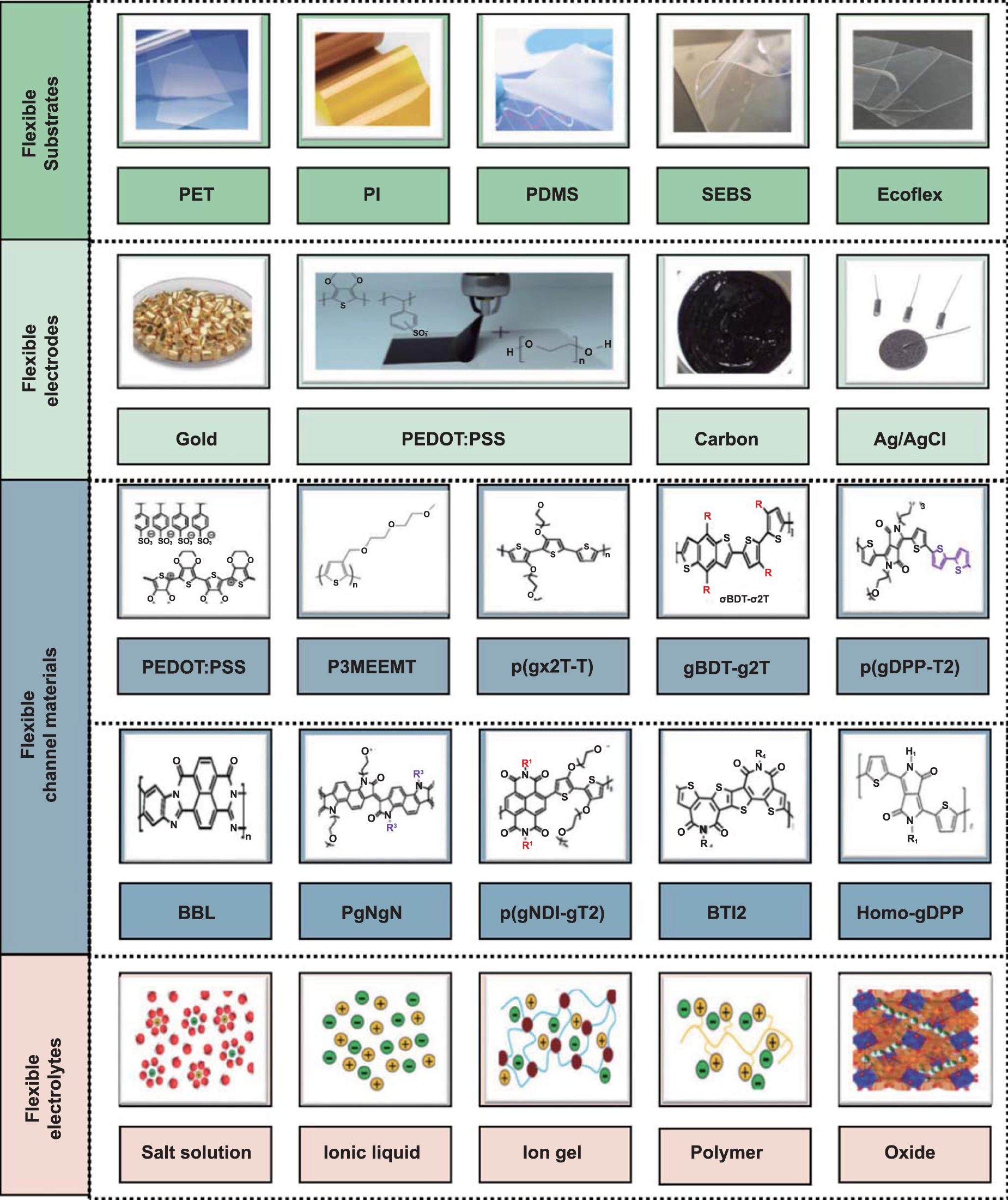
Not only electrical properties but also mechanical characterizations (such as flexibility, stretchability and elasticity) of functional materials should be taken into account when using flexible OECTs in skin-integrated devices in vitro and implantable devices in vivo. In this part, we present a comprehensive summary of the representative examples of functional materials used in flexible and stretchable OECTs from four aspects: substrate, electrodes, organic semiconductors, and electrolyte, as depicted in figure 3.

Figure 3. Commonly used representative examples for flexible OECTs, including substrates, electrodes, p- and n- type channel materials as well as electrolytes.
Download figure:
Standard image High-resolution image3.1. Flexible materials
As the foundation of flexible OECTs, substrates are required to have excellent tissue conformability and mechanical stability so as to fit the non-planar and malleable surfaces. Polymers, such as polyimide (PI) and polyethylene terephthalate (PET) [33, 53, 98, 99], are most commonly used as substrates due to their unique combination of mechanical, chemical, and thermal properties. Note, bending radii and substrate thickness affect the mechanical strain on the surface of functional materials [20]. Hence, micro- or nano-scale films prepared from brittle materials (such as ceramics, glasses, or certain types of polymers) can be bent to a certain extent, offering more possibility and scalability for flexible substrates. The choice of substrate depends on the specific requirements of the device, such as mechanical flexibility, electrical performance, transparency, and compatibility with other device components. Different substrates may be selected based on the intended application and desired performance characteristics of the OECT.
Electrodes (gate, source and drain) materials are one of the key elements for the construction of flexible OECTs. As described above in the section on working mechanism, a gate electrode with efficient gating ability is crucial for realizing excellent transconductance performance. In general, PEDOT: PSS-modified gold and non-polarized Ag/AgCl are commonly used as gates [96]. In addition, conductive polymer (PEDOT: PSS) and carbon material (graphene and carbon nanotubes) have also been explored as gate materials in flexible OECTs [100, 101], and the OECT electrochemical performance based on traditional and novel gate materials depends on the specific application requirements and the specific material used. On the other hand, source and drain electrodes should possess capabilities of intrinsic flexibility, high conductivity, suitable Fermi level, low contact resistance with semiconductors, and desirable biocompatibility. Metallic materials offer great conductivity but are mostly electrochemically unstable (e.g. sliver and aluminum). It is challenging to achieve a long-term stability in OECT devices using such unstable metals. Because if the electrode material is electrochemically unstable, it can react with the electrolyte or the transistor channel, leading to changes in the device performance or even complete device failure. Therefore, Au is the most representative electrode in flexible OECT. Tremendous polymer electrodes have also been developed for flexible OECTs, such as polypyrene, polyaniline, and polythiophene [102, 103]. However, studies on flexible OECTs are still in their infancy, resulting in less focus on polymer electrodes.
Organic semiconductors possess mechanical flexibility and a customizable molecular structure that facilitates efficient coupling and transport of ions and electrons. These channel materials typically have conjugated backbones and side chains for electron conduction, making them readily amenable to ion intercalation from the electrolyte being manipulated. And their low Young's modulus values (5 kPa–140 MPa) are similar to those of living tissue (0.1 kPa–1 MPa) [104], are far below the high modulus values of inorganic semiconductors (>10 GPa) [105]. According to the doping modes of the channel material, it can be divided into two types: p-type, which exhibits an excess of positively charged holes, and n-type, which exhibits an excess of negatively charged electrons. A commercial p-type material commonly used for flexible OECTs is PEDOT: PSS because of its low loss, biocompatibility and flexibility [99, 106, 107]. To some extent, materials engineering towards the molecular design of side chains, backbones and other additives opens up design space for breakthroughs in enhancing OECT material properties [78, 108, 109]. Thus, both p-type and n-type semiconducting materials have been gradually designed. However, the majority of high-performance OECT channel materials are derived from previously reported polymer structures used in organic field-effect transistors. Typical p-type polymers include poly(3-{[2-(2-methoxyethoxy)ethoxy]methyl} thiophene-2,5-diyl) and poly(2-(3,3-bis(2-(2-(2-methoxyethoxy)ethoxy)-ethoxy)-[2,2ʹ-bithiophen]-5-yl)thieno[3,2-b] thiophene) (P3MEEMT and P(g2T-TT)), etc [74, 110, 111]. Additionally, in addition to Poly(benzimidazobenzophenanthroline) (BBL) and the recently published PgNgN, the predominant n-type systems extensively examined are founded on naphthalenediimide derivatives [45, 75, 112], as illustrated in table 3. As for active channel materials, π-conjugated polymers or small molecules are fabricated by solution methods [113], such as spin-coating [114] and blade-coating [115]. Furthermore, various preparation strategies have been demonstrated to optimize the OECT electrochemical performances. Interfacial engineering (small molecule additives [116] and mixed solvents [117]) and post-treatment (annealing [110]) and acid treatment [118]) can effectively reduce surface traps, improve chain aggregation, and increase charge carrier mobilities. Therefore, through materials engineering, the newly designed and synthesized p- and n-type organic semiconductor materials are desired to enhance the output performance and mechanical stability in flexible OECT devices.
Table 3. Comparation of typical p- and n-type OECT materials.
| OMIECs | Materials | Advantages | Disadvantages | μC* (F cm−1 V−1 S−1) | References |
|---|---|---|---|---|---|
| p-type | PEDOT: PSS | High conductivity | Poor stability | 47± 6 | [119] |
| Transparency | High consumption | ||||
| P3MEEMT | Biocompatibility | Low stability | 49 ± 5 | [110] | |
| Large volumetric capacitance | |||||
| P(g2T-TT) | High mobility | Complexity of synthesis | 261 ± 29 | [120] | |
| Low operational voltage | |||||
| n-type | BBL | Reliable stability | Brittle | 26 ± 3 | [75] |
| Large volumetric capacitance | Limited solubility | ||||
| PgNgN | Nontoxic synthesized | Low mobility | 0.66 ± 0.11 | [112] | |
| Poor stability | |||||
| HOMO-gDPP | High mobility | Synthesis complex | / | [14] | |
| Ultra-High stability |
The electrolytes play critical effects in the whole OECT device. First, electrolytes provide wandering ions which dominates device capacitance, switching time, and operating voltage. Then electrolytes determine the system flexibility when OECTs are integrated with other intelligent systems. Electrolyte materials can be the forms of liquids, solids or gels, all of which have intrinsic mechanical flexibility to facilitate the integration of flexible OECT devices in bio-interface and sensing applications [11, 121, 122]. Aqueous salts and ionic liquids (ILs) are typical liquid electrolytes, whereas salt type and concentration would result in various solvation shells that obviously affecting the output performance. By contrast, ILs are composed entirely of anions and cations. Although liquid electrolytes allow efficient gating and faster response times, the intrinsic liquid environment limits a wider range of applications. Therefore, ion gels as a semi-solid compound that maintains high ion mobility owing to the incorporation of an IL into the crosslinked polymer network, have been commonly employed to fabricate flexible OECTs. Besides, polymer electrolytes and polyelectrolytes (triblock copolymer (PS–PIL–PS)), as solid electrolytes are capable of providing the transport of ions mobile, can also exhibit excellent capacitance (∼1 μF cm−2) performance in OECT devices [123].
3.2. Stretchable materials
Besides, stretchability is vital and highly expected for numerous applications, such as skin-mounted biosensors and tissue-conformal bioelectronics. It is well known that stretchable devices are extensions of flexible devices, since the stretchability enables the device to easily conform to the deformable human tissue, especially for tensile deformations, such as the movement of the elbow joint in vitro and contraction–relaxation of the heart in vivo. Such a property enables intimate contact between the electronic devices and the active tissues during the tensible deformation, which avoids motion artifacts and enhances the detection accuracy [35, 124]. The stretch limit of device depends on the substrate since most of the stress is dispersed here. Typical substrates used for stretchable OECT are poly(dimethylsiloxane) (PDMS), and polystyrene-block-poly(ethylene-ran-butylene)-block-polystyrene (SEBS) and EcoFlex elastomers [82, 125, 126]. Moreover, fiber and textile have been utilized as stretchable substrates, such as elastic cotton fiber and nylon [127, 128], which allows for the development of wearable electronics that can be comfortably worn on the body while maintaining stretchability.
Stretchable electrodes in OECTs that can undergo mechanical stretching or deformation without compromising its electrical performance is the most basic requirement. To make stretchable electrode for OECTs, researchers often employ elastic conductive materials that can withstand mechanical strain while maintaining good electrical conductivity. Commonly used stretchable electrode is Au, tremendous efforts has been made to offer Au stretchable via strain-dissipative geometries, such as transfer gold electrode to pre-stretched substrate, design honeycomb grid structures and synthesis gold nanowire networks [82, 129–131]. More recently, PEDOT: PSS, a conductive polymer inherently brittle due to its relatively high crystallinity, has been successfully engineered to be stretchable OECT electrodes by blending it with surfactants or plasticizers [107, 126]. However, PEDOT: PSS, as a typical transistor channel material with electrochemical activity, should be further considered when used as the source and drain electrodes. In addition to the choice of stretchable conductive electrodes, the design and fabrication methods play a crucial role in creating stretchable electrodes for OECTs [132]. Techniques like printing, or solution processing can be further used to pattern or deposit the electrode materials onto substrate substrates. These methods allow for the fabrication of stretchable electrodes with controlled dimensions and desired properties. Overall, the development of stretchable electrodes for OECTs is an active area of stretchable OECT, aiming to enable the integration of electronic devices with soft and deformable materials for applications.
Stretchable semiconductors are an emerging field of research in OECT that aims to develop mixed ionic-electronic coupled materials capable of stretching and conforming to various shapes without compromising their functionality. Several approaches including strain engineering, microstructure engineering, or packing structure engineering have been explored to develop stretchable semiconductors for OECTs, one of the most commonly used materials for stretchable OECT is PEDOT:PSS [108, 129–131, 133], which offers the combination of high conductivity, processability, mechanical flexibility, and ion transport properties. However, PEDOT:PSS, being a heavily doped conjugated polymer, can only operate in depletion mode, which is not desirable for low power consumption. Substantial progress has recently been focused on the development of non-doped redox-active semiconductor polymers (DPP-g2T, Pg2T-T) [78, 82], which not only lead to the operation of OECTs in enhancement mode, but also improve the electrochemical properties such as electrical performance, stability, etc. These polymers are typically synthesized to have a stretchable molecular structure, allowing them to withstand mechanical deformation. Besides, in terms of microstructure design, conventional three-dimensional (3D) porous elastic semiconductor films based on P3HT can improve both ionic-electronic coupling transport properties and mechanical tensile properties [15, 16]. Although some progress has been realized with stretchable OECT semiconductor materials, addressing challenges related to soft material design, stability, fabrication, and performance trade-offs is critical to their successful implementation in future OECTs.
4. Manufacturing approaches for OECTs
The development of commercially available OECTs that are flexible, scalable, and consistently reproducible demands the establishment of robust manufacturing strategies. In this section, a variety of advanced manufacturing approaches have been summarized, encompassing methods such as photolithography, a well-established process involving light exposure to create patterns, as well as diverse printing techniques that offer promising scalability and cost-effectiveness [18].
4.1. Photolithography
Photolithography technique represents the core process for manufacturing electronic devices. It is particularly important for OECT devices, as the active area must be small enough to provide high on/off ratios and fast transient times, yet large enough to allow efficient charge transport [14, 90, 134–136]. In addition, photolithography provides a cost-effective method of fabricating high-density OECT arrays, making it an ideal candidate for multichannel and nanoscale bioelectronics [85, 137–139]. The photolithography technology typically involves five steps, including photoresist coating, ultraviolet light exposing, developing, etching, and photoresist removing (figure 4(a)). It should be addressed that the above process is repeated several times, as needed, to produce a multilayer OECT device. In a typical fabrication approach for OECT, the substrate is initially coated with a uniform organic mixed ionic–electronic coupled and transport semiconductor, followed by patterning the semiconductor via photolithography and etching [18].
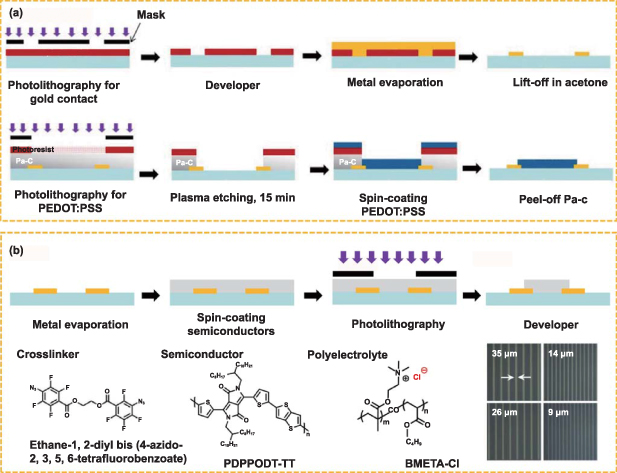
Figure 4. Two typical photolithography techniques for OECT fabrication. (a) Conventional photolithography technique for OECT, typically involves several steps, including substrate preparation, active layer coating, exposure, development, etching, and substrate cleaning. (b) Novel photolithography technique for patterned semiconducting films with high resolution (sub-10 nm), including the chemical structures of semiconducting polymers, polyelectrolyte, and redox-inactive cross-linkable polymer, as well as SEM image of patterned semiconductors. Reprinted from [122], with the permission of AIP Publishing.
Download figure:
Standard image High-resolution imageConventional photolithography techniques are conducted under the assisted of photoresists (such as AZ4620, AZ5214, and SU8), and the precision of photolithography depends on lithography machine, the physicochemical properties of the photoresist, and the etching speed of the material being lithographed. Photolithography techniques is paramount for advanced micro-, nano- OECT devices due to its ability to impart high precision and accuracy, enabling the creation of intricate structures with fine details. For instance, Jimbo et al demonstrated a record channel length as small as 5 μm via the liftoff process [140]. Typical performance gm of two milliSiemens (mS), and fast response time of 62 μS have been achieved. Wu et al developed 100-channel OECT arrays in 64 mm2 by continuous photolithography processes [38]. And yielded excellent spatiotemporal resolution of 1.42 ms and 20 µm and tissue-compatible mechanical properties, enable OECT an efficient neural interface for mapping rats' brain activity. In addition, Takao Someya research group developed a transparent and ultraflexible OECT array via photolithographically prepared Au grid wirings, where 1.2 µm perylene was used as substrate [37]. The micropatterned Au grid (with a 3 µm linewidth) exhibited 60% transparency at 475 nm, which offers a technology road for mapping evoked responses from optogenetic rats. Besides, great mechanical durability was verified by cyclic tests of sheet resistance.
However, limitations of conventional photolithography techniques still exist in their application to organic semiconductors, including material incompatibilities and vulnerabilities during solution handling, which hinder the miniaturization and scalability of organic electronics. This results in a significant lag in the advancement of organic electronics compared to silicon electronics. Especially for using in flexible OECTs, process compatibility, device scale, and photolithography precision should be taken into account [141]. The photoresist processes (such as photoresists, developers, and photoresist-removers) may corrode the organic functional materials [136]. On the other hand, the quality of organic films can affect the spin-coating of photoresist, leading to a negative effect on pattern fidelity. Consequently, un-uniform and defective organic films are obtained, which will result in poor electrochemical performance and operation stability. Besides, the minimum accuracy of the photolithography process is on the sub-micro scale, leading to large channel lengths and low transconductance values of OECTs. This is due to the fact that the transconductance values of OECTs are not only determined by the physicochemical properties of channel materials but are also related to the device size. Specifically, OECT with short channel length and large channel width enable greater transconductance [3, 5].
Thus, the development of foundry-compatible organic semiconductors patterning methods that maintains device performance has potentially revolutionize the OECT industry [142, 143]. Recently, Kwak et al reported photo-patternable organic mixed ionic and electronic conductors (OMIECs) by introducing a photocross-linkable material (thane-1,2-diyl bis(4-azido-2,3,5,6 tetrafluorobenzoate)) into ion-conducting conjugated polymers to address these challenges (figure 4(b)). When this cross-linker is used in polymer cross-linking reactions, the azide group (–N3) is usually involved in the reaction and can react with a suitable alkyl-functionalized polymer or molecule containing an alkyl molecule. This chemistry of the cross-linking reactions involving azido compounds relies on the highly efficient and selective click chemistry reactions, enabling the formation of stable and robust cross-linkages in polymer networks. The patterning technique is exceptionally efficient as it only necessitates three steps, making the manufacture process simpler than conventional photolithography [142], in which a blend film of semiconductor/electrolyte and crosslinkers can be patterned directly via UV light-triggered crosslinking. With this patterning technology, flexible OECTs were evaluated and presented high carrier mobility (3.4 cm2 V−1 s−1) and reliabe mechanical stability, with minimal degradation in OECT output performance, even after undergoing 5000 bending cycles at radius of only 0.1 mm. Similar photo-crosslinker also have been conducted in advanced vOECT [14], Huang et al proposed photo-patternable OMIECs by introducing cross-linkable material (Cin-Cell) into ion-conducting conjugated polymers. Vertical OECTs were evaluated with footprint current densities of more than 1 kA cm−2 at less than ±0.7 V input voltage, transient times shorter than 1 ms, transconductances up to 0.2–0.4 S and stable on/off switching (>50 000 cycles) are realized simultaneously. Such lithography technique has achieved remarkable progress, future work focus on patterning OECT can start from the following directions: (1) introduction of crosslinking agents to enhance lithography performance also requires attention to the balance of electrochemical properties. (2) Scalability of photocrosslinking has not been systematically demonstrated, and achieving high-resolution and stable crosslinking through semiconductor materials and electrolytes is critical. Photopatterning semiconductors and electrolytes enables precise, scalable creation of multifunctional OECTs compatible with established fabrication techniques, including solid-state integrated circuits, neuromorphic computing, and bioelectronics. The challenges include, first, developing suitable photosensitive materials and understanding their compatibility with electrolyte formulations; second, optimizing the photopatterning process to achieve high resolution and minimal photodamage is critical for practical implementation. (3) Limited by the structural complexity and lack the necessary functional groups or reactive sites to undergo efficient crosslinking of small molecule semiconductors, currently available photocrosslinkers are mainly for polymeric semiconductors, therefore, in the future there is a need to develop efficient crosslinkers via molecular engineering design that can crosslink not only in polymeric semiconductors, but also in small molecule semiconductors. These critical advances in photolithography and photo-patterning of OECTs provide insights for the future commercialization of stable integrated organic devices.
4.2. Printing
Printing technologies have also attracted significant interest in flexible OECT devices, as pairing functional materials with printing technology enables to achieve high-throughput, large-scale and low-cost electronic devices [32, 144–146]. Well-known printing technologies including screen printing [32, 81, 147–150], inkjet printing [151–153], 3D printing [79, 154], transfer printing [107, 155], and aerosol jet printing [156, 157] have been implemented to fabricate flexible OECTs. Each printing technique needs ink with different physical or chemical parameters and offers different resolutions for functional patterns. For example, screen printing, typically uses inks with high surface tension and viscosity, as well as good adhesion to the substrate and durability. Inkjet printing, on the other hand, typically requires inks with lower viscosity and surface tension, as well as good solubility and stability in the inkjet printer's ink reservoir. Notably, the resolution of screen printing is generally lower than inkjet printing, as it relies on the mesh count and thickness of the ink. Therefore, it is crucial to consider the most suitable inks and printing method to obtain the desired functional films. Figure 5(a) illustrates a representative screen-printing process, first depositing the silver ink on the target flexible substrate (PET) to provide the probe contact pads and enhance conductivity. Next, PEDOT: PSS ink is deposited via screen printing as designed pattern to ensure directly contact with the source-drain electrodes (usually carbon conductive materials). Most critically, printed gel electrolytes or solid electrolytes that connecting gate and channel are required for high performance OECTs. Finally, the PEDOT: PSS gate is printed to form the OECT devices [81]. Compared to the high resolution (in several or tens micrometers) and limited device size of the photolithography process, printing technologies enable large-scale fabrication, but with low resolution (in millimeters and centimeters).
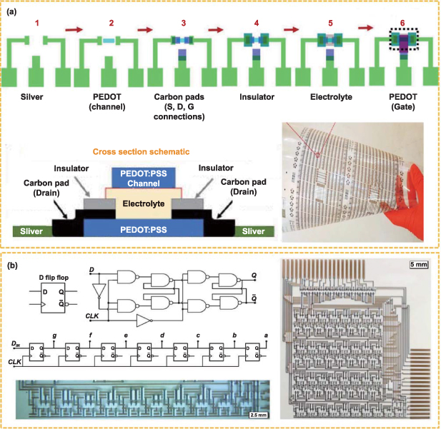
Figure 5. Screen printing techniques for OECT fabrication. (a) Scheme illustration of OECT fabrication process based on all screen-printing technique and corresponding device. Reproduced from [81], with permission from Springer Nature. (b) Illustration of a 4-to-7 decoder achieved by NAND gates and inverters, and a photo of the fully printed decoder with 87 OECTs. Reproduced from [32], with permission from Springer Nature.
Download figure:
Standard image High-resolution imagePrinted flexible OECTs enable the efficient manufacture of large-scale, cost-effective electronic devices and seamlessly integrated systems, offering significant potential for driving innovative applications within the domain of flexible electronics. As for screen-printing, Ersman et al demonstrated large-scale (8 × 9 cm2) integrated circuits (4-to-7 decoder and seven-bit shift register) by sequentially screen-printed coplanar flexible OECTs (figure 5(b)). Such printed OECTs exhibit a low operating voltage of 0.5 V and excellent uniformity of electrical performance (variation as low as 1%), providing a facile large-scale manufacturing route towards advanced Internet of Things applications [32]. More recently, screen printed flexible OECTs have also been reported for using as artificial spiking neural circuits [150]. Simone et al screen-printed Ag 5000 silver ink (source-drain electrodes) and insulating 5018 ink (dielectric layer) onto PET substrates via screen-printing equipment. And they blade-coated Ag/AgCl ink (as the gate) and spray-casted P(g2T-T) and BBL (as the channel) through shadow masks. The successful demonstrations of short-term and long-term plasticity (LTP) (retention >1000 s) offer printed OECTs a new perspective for artificial neural systems that could be integrated with bio-systems.
Although numerous research have proved the availability of OECTs fabricated via screen printing techniques, there is also an urgent need for other printing techniques to meet the growing demand and enable high-throughput preparation of material and device concepts. In sight of this, inkjet printing holds several advantages over commonly used screen printing, as it offers enhanced flexibility in selecting materials, preparing functional inks, and designing patterns. To optimize the pliability of the gold electrodes in OECT located on wavy surfaces, a semiconductor layer with exceptional conductive properties has been delicately applied via inkjet printing onto the Au surface (figure 6(a)). This process effectively connects the disjointed sections that were previously isolated by cracks. The resultant flexible OECTs exhibit stretchability of up to 30%, while retaining reliable performance even when bent to a radius as small as 15 mm [152]. In addition, inspired by the natural world, inkjet printing for producing OECTs has also been presented to generate semiconducting thin films (figure 6(b)), with the ultimate goal of achieving high-performance devices. These remarkable flexible OECTs exhibit depletion mode operation, coupled with pulse depression behavior, showcasing compelling evidence of their adaptability and reinforcing their potential as neuromorphic electronics [153]. It is worth noting that 3D printing technology was also introduced in this work, 3D printing is that it allows for the creation of highly detailed and intricate designs with speed and accuracy, making it a versatile and efficient OECT manufacturing strategy. For example, Fan et al presented a fully 3D printed flexible OECTs via PEDOT:PSS inks as transistor channel and silver as source and drain electrodes (figure 6(c)). High transconductance (∼31.8 mS), low working voltage (∼0.1 V) and high current ON/OFF ratio (∼1.33 × 10³) can be realized [154]. 3D-printed OECTs can also be manufactured on flexible substrate with high environmental and mechanical stabilities for biosensor applications (figure 6(d)) [79].
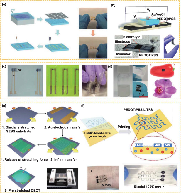
Figure 6. Printing techniques for flexible OECT. (a), (b) Scheme illustration of OECT fabrication process based on inkjet printing technique and corresponding flexible/stretchable devices. [152] John Wiley & Sons. © 2019 WILEY-VCH Verlag GmbH & Co. KGaA, Weinheim. [153] John Wiley & Sons. © 2020 The Authors. Advanced Materials Technologies published by Wiley-VCH GmbH. (c), (d) Optical images of flexible OECTs based on 3D printing technique. Reprinted from [154], Copyright (2019), with permission from Elsevier. Reproduced from [79], with permission from Springer Nature. (e), (f) Schematics of flexible OECT based on transfer printing technique. Reproduced from [82], with permission from Springer Nature. Reproduced from [107], with permission from Springer Nature.
Download figure:
Standard image High-resolution imageDue to the low glass transition temperature, conventional metal electrodes cannot be deposited easily onto stretchable elastomer substrates with reliable mechanical performance. To solve this problem, Chen et al transfer-printed Au electrodes and free-standing honeycomb films (poly(2,5-bis(2-octyldodecyl)-3,6-di(thiophen-2-yl)-2,5-diketo-pyrrolopyrrole-alt-2,5-bis(3-triethyleneglycoloxy-thiophen-2-yl)), DPP-g2T) on pre-stretched SEBS substrates [82]. As shown in figure 6(e), outstanding electrochemical and mechanical properties have been obtained, including high ON-OFF ratio up to 105, normalized peak gm up to (24.91 ± 1.47) S cm−1, and more than 1500 switching cycles under 30% tensile strain. Wang et al also presented a general platform via transfer printing LiTFSI doped PEDOT: PSS to an elastic gelatin electrolyte (figure 6(f)), elastic OECTs with high transconductance (∼12.7 mS), mechanical stability, long-term environmental durability, and sustainability are realized simultaneously [107]. Therefore, transfer printing of OECTs offers several advantages, including high-resolution printing with excellent durability. It is also versatile and applicable to an extensive range of materials and shapes, allowing for greater design flexibility. Additionally, transfer printing allows for efficient production and reduces waste, making it a cost-effective option for businesses.
Although the use of printing technology has certain merits in terms of large-scale production and related application, the challenges and opportunities inherent in the situation require further addressed. The resolution of the printing technology utilized in OECT is limited, and conventional printing with feature line widths and spacing in excess of 10 μm means that smaller patterning accuracy is difficult to achieve, thus developing new printing technology to break through resolution is highly expected. The second is the limitation of printing OMIEC materials, with respect to the most widely used PEDOT: PSS materials, more efficient ionic–electron coupled and transport materials for printing need to be further developed.
The manufacturing techniques for OECT devices are highly relied on the device structure and functional materials, and the output performance of the fabricated devices exhibit significantly batch to batch variations. For example, table 4 demonstrates the broader applicability of photolithography to a variety of semiconductor materials beyond PEDOT: PSS. In contrast, printing technologies may exhibit restrictions with respect to the selection of functional materials and the attainment of desired electrical and mechanical performance. However, by designing the device structure carefully, it is possible to achieve significant improvements in device performance. Especially, vertical structures can exhibit performance levels in the milliampere range (approximately 1–3 orders of magnitude enhancement), which opens up new avenues for the development of OECT manufacturing technology.
Table 4. Summary of typical examples of flexible OECTs.
| Manufacture techniques | Device structure | Functional materials | Electrical performance | Mechanical performance | References |
|---|---|---|---|---|---|
| Photolithography | Vertical | PET/Au/PEDOT: SS/AgNWs/Ion gel/Au | gm = (64.25 ± 1.49) mS | Radius 10 mm, 1000 cycles | [92] |
| on/off ratio ∼ 100 | |||||
| τon ∼ 0.3 ms, τoff ∼ 1 ms | |||||
| Photolithography | Top-gated | PDMS/Au/PEDOT: PSS/PBS | gm = 0.432 mS | 60% strains | [125] |
| Signal-to-noise | |||||
| ratio of 12.2 dB | |||||
| Photolithography | Side-gated | PET/Au/PEDOT: PSS/PBS | Signal-to-noise ratio of 3 dB | Bendable | [137] |
| τon ∼ 0.6 ms, τoff ∼ 3 ms | |||||
| Photolithography | Top-gated | PET/Au/ PDPPODT-TT/BMETA-Cl/Au | gm = 15.1 μS | Radius 0.1 mm, 5000 cycles | [142] |
| on/off ratio ∼ 2 × 10⁵ | |||||
| Photolithography | Top-gated | Parylene/AgNWs- PEDOT: PSS/PEDOT: PSS/PBS | gm = 1.0 mS | Radius 0.8 mm | [158] |
| Printing | Top-gated | SEBS/Au/DPP-g2T/KPF6 | gm = (2.47 ± 0.24) mS | 150% strains | [82] |
| on/off ratio ∼ 105 | 1500 cycles | ||||
| Printing | Side-gated | PET/Carbon/PEDOT: PSS/PSSNa | on/off ratio ∼ 105 | Bendable | [32] |
| τon ∼ 30 ms, τoff ∼ 20 ms | |||||
| Printing | Side-gated | Cellulose/Carbon/PEDOT: PSS/PSSNa + NaCl | gm ∼ 70 S·cm−1 | Bendable | [149] |
| on/off ratio ∼ 103 | |||||
| Printing | Top-gated | PET/Carbon/PEDOT: PSS/polyelectrolyte | on/off ratio ∼ 104 | Bendable | [81] |
| τon ∼ 20 ms, τoff ∼ 225 ms | |||||
| Printing | Side-gated | PDMS/Au/PEDOT: PSS/PBS | on/off ratio ∼ 100 | 30% strains | [152] |
5. Applications of flexible OECT
Flexible OECTs are regarded as the solid foundation for bioelectronics applications owing to their intrinsic signal amplification, low power consumption, and excellent biocompatibility. With the continuous evolution of flexible materials and advanced manufacturing, substantial progress of OECTs have been achieved in bioelectronics, especially for biocompatible sensors and bioinspired neuromorphic systems. This section focuses on three bioelectronics applications of flexible OECT, including physical/chemical/biosensors, artificial synapses and neurons, and biomimetic nervous systems.
5.1. Physical, chemical and biosensors
OECT-based flexible physical sensors have been developed to detect pressure, light, as well as temperature, which are expected to real-time monitor biological indicators such as tactile touch, blood pressure, body temperature, etc [37, 139, 159–162]. For instance, as illustrated in figure 7(a), Chen et al demonstrated a flexible OECT for sensitive haptics sensing, employing a solid polymer electrolyte of EMIM-TFSI doped PVDF-co-HFP that promotes reliable and stable electrochemical response of PEDOT: PSS and P3HT [159]. Such sensor showed high sensitivity (10 828.2 kPa−1), excellent stability of (more than 2 months' operation), low limit of pressure detection (1.1 Pa), and ultra-low power consumption (<5 µW). Attributed to the reliable flexibility, reproducibility, durability, and scalability of OECT haptic sensor, a 6 × 6 pixel flexible pressure sensor array was demonstrated to capture temporal and spatial pressure distributions. The results presented here suggest that all-solid-state OECTs are promising candidate for sensing haptic signals for health monitoring and human–computer interaction interfaces. Meanwhile, large-area, high-density OECT tactile sensory array with skin-like functions via the combination of advanced manufacturing processes is highly expected.

Figure 7. Physical, chemical and biological sensors based on OECT. (a) All-solid-state flexible OECTs with contact-modulated ion doping modes for ultra-sensitive haptic sensor. [159] John Wiley & Sons. © 2020 Wiley-VCH GmbH. (b) High sensitive OECT-based gas sensor for wireless and continuous NO detection. Reproduced with permission from [163]. (c) Sensitive, ultrafast and portable monitor of COVID-19 IgG using flexible OECT-based biosensors. From [137]. Reprinted with permission from AAAS.
Download figure:
Standard image High-resolution imageChemical sensors are instruments that are sensitized to various chemical substances (such as chemical molecules, ions, and gases) and translate their concentrations into corresponding electrical signals for detection. Analogous to the human sense organs, chemical sensors correspond to the human sense organs of smell and taste, which can also sense certain substances that cannot be sensed by human organs, especially special ions (e.g. Ca2+, K+, Na+, Cl−) and gases (e.g. NO, NO2, H2S) related to the physiological state of the body [52, 163–166]. For example, NO exhibits functions that are essential in biological systems, which is thought to be a physiological mediator of endothelial cell diastole and has a significant role in lowering blood pressure. The continuous detecting of NO gas is of tremendous concern for therapeutic and diagnostic applications. Deng et al proposed a flexible, wireless NO sensor via OECT device, typically, the oxidation reaction of NO, which takes place at the gate, serves as a contributing factor to the increase in potential at the interface between the channel and electrolyte. This dedoping process becomes evident through a decrease in the drain current. Wide sensing range of 0–1 μM and high sensitivity up to 94 mV dec−1 have been achieved, which far exceed those of conventional sensors (figure 7(b)). It is encouraging to note that the OECT-based sensor device accomplished wireless and real-time detecting of NO in the joint cavity in 8 d, which could provide important evidence for early preventive treatment and diagnosis of post-traumatic bone and joint injuries [163]. Hence, the development of more in vivo and in vitro flexible/stretchable sensing platforms based on OECT for chemical signal sensing is important for healthy environment and disease prevention. Furthermore, chemical ion sensors provide valuable information on the presence and concentration of specific ions, from environmental monitoring to biomedical analysis, which is important for monitoring human health processes. Pierre et al showcased an integrated system, representing a significant advancement in the realm of ion sensing, that encompasses miniaturized ion-selective flexible OECTs and a straightforward multiplexed circuit [165]. The resulting flexible sensor array allows the monitoring of multiple ions at high resolution, maintains relatively stable OECT performance at a curvature radius of 1.1 mm, making it a valuable tool in various fields, including environmental monitoring and biomedical research. This OECT technology has the ability to revolutionize the way we can monitor and analyze ions in a variety of environments, ultimately enhancing our comprehension and regulation of chemical processes both in the natural world and in human health.
Biosensors are instruments that are sensitized to various biological substances and translate their concentrations into corresponding electrical signals for monitoring. It is composed of immobilized and specific biosensitive materials as identification elements for analytical tools or systems (including enzymes, metabolite, antigens, antibodies, nucleic acids, tissues, cells, and other bioactive substances) [137, 158, 167–169]. OECT devices serve as the fundamental building blocks of biosensing, enabling objective measurement and evaluation of biomarkers. These biomarkers serve as indicators of disease or normal processes within biological systems, as well as being closely associated with the pharmacological response to therapeutic agents. Typically, with the emergence of COVID-19 outbreak and continued spread has become a serious threat to public health, rapid detection of antibody biomarker is critical for diagnostic analysis of viral infections. Liu et al constructed an ultra-fast, label-free, low-cost, portable and wireless platform for SARS-CoV-2 immunoglobulin G (IgG) detection via miniaturized OECT technology with gate functionalization in figure 7(c). The principle of rapid detection involves enhancing the binding between the antigen and antibody by applying a voltage pulse to the OECT gate electrode. A specific assay for detecting SARS-CoV-2 IgG was conducted within minutes, encompassing a detectable range from 10 fM to 100 nM. This range effectively covers the levels of SARS-CoV-2 IgG found in human serum [137]. To some extent, OECT-based biosensors can overcome the drawbacks of conventional devices, such as bulky and immobilized assays, and contribute to the rapid prediction, screening, diagnosis and treatment of diseases.
Multimodal sensing capabilities are indispensable in bioelectronic applications for complicated diagnoses and smart healthcare. In general, multimodal neuromorphic devices with multiple perceptual abilities are realized by integrating multiple sensing units [72, 170, 171]. For example, as illustrated in figure 8(a), Takemoto et al integrated a fully transparent flexible OECT with a photodetector, near-infrared laser, and micro-light-emitting diode (μ-LED) to monitor mental stress from the perspectives of electrophysiological, optical, and ionic methods [170]. To obtain electrical signals for electroencephalogram sensing, the human forehead can be utilized both before and after the eyes are opened, and they were employed to the OECT gate, leading to the variation of drain current. For blood flow sensing, a vertically placed laser Doppler flowmetry was used, and the near-infrared laser (∼780 nm) from μ-LED can easily be transmitted by OECT due to its high transparency (∼90%). For the ion sensing of nitrate, ion-selective electrodes were chosen to modify the gate in order to enhance sensitivity, and a high sensitivity of 2.2 μA dec−1 was obtained. Furthermore, regulations for measurement conditions and device configuration have been reported for the realization of multimodal neuromorphic devices. Strand et al introduced DC modes (resistive, potentiation, and potentiodynamic) and AC modes (electrochemical impedance spectroscopy and square wave voltammetry) simultaneous detection of electrical conductivity, pH and temperature of active hydroponic growth environment with single device (figure 8(b)) [171]. As shown in figure 8(c), Wang et al implanted a crystalline–amorphous channel (PTBT-p) of OECT that can be selectively doped in the volatile and non-volatile modes [72]. In volatile mode, OECT synapses demonstrate the ability to detect multi-modal signals, including light and ions. In non-volatile mode, these synapses exhibit 10-bit analog states, excellent state retention and low switching stochasticity.

Figure 8. Flexible OECTs for the application of multimode sensors. (a) Cross-sectional illustration and optical image of the integrated multi-mode OECT-based system. [170] John Wiley & Sons. © 2022 The Authors. Advanced Science published by Wiley-VCH GmbH. (b) Experimental setup for gate impedance measurements and square wave voltammetry measurements, and the optical image of printed flexible OECT sensors. Reprinted from [171], Copyright (2023), with permission from Elsevier. (c) Ionic contribution in volatile/non-volatile modes, and schematic illustration of crystalline vertically (cv)-OECT as volatile multi-mode sensor, as well as the optical image of flexible cv-OECT. Reproduced from [72], with permission from Springer Nature.
Download figure:
Standard image High-resolution image5.2. Synapse and neuron emulation
Neuromorphic engineering aims to create brain-inspired systems via emulating the structure and function of biological neural networks. One crucial element of such systems is the advancement of proficient and scalable artificial synapses and neurons that emulate the biological synaptic behaviors, encompassing short-term plasticity (STP), LTP, paired pulse facilitation (PPF), and paired pulse depression (PPD). Such bioinspired artificial synapses and neurons play significant roles in achieving sensory functions, memory storage, and computational capabilities. Recently, OECTs have been implanted in various neuromorphic devices, and exciting advancements have been obtained. Therefore, this section presents a comprehensive overview of the most recent advancements in flexible synapses and neurons based on OECT technology.
For synapses in biological nervous systems, signals are achieved via the exchange of different molecular species or ions. The presynaptic membrane contains a large number of synaptic vesicles encapsulated with neurotransmitters that accumulate in the active zone of the presynaptic membrane. Once the action potential reaches the presynaptic membrane, the synaptic vesicles moored in the active zone fuse with the cytoplasmic membrane and releasing neurotransmitters into the synaptic gap and captured by postsynaptic membrane receptors, thus enabling the transmission of information. OECTs can serve as alternative platforms for artificial synapse emulation due to their structural properties of physical separation input and output terminals [25, 27, 92, 172, 173]. Thus, synaptic weight (channel conductivity, G) can be accurately modulated in a capacitance coupling manner between the transport (source and drain electrodes) and the control (gate electrode) terminal. Through sequential read or write processes via pulse voltage, it is desirable for synaptic transistors to decouple STP and LTP, thus becoming a natural and appropriate medium wherein both synaptic STP and LTP can be independently induced and expressed. Van De Burgt et al initially reported the flexible synaptic OECT, which comprises postsynaptic electrode, the PEI/PEDOT:PSS film, and is connected to the presynaptic electrode of PEDOT:PSS via a liquid electrolyte (figure 9(a)). The results showed that the device exhibits a series of synaptic functions, which are worked as essential building blocks for neuromorphic computation. To indicate the modulation of the non-volatile state of the mimicked synapses, a series of 500 pulsed gate voltages were also applied to produce 500 different conduction states, indicating their short- and long-term plasticity. Besides, as a simple demonstration of the learning function, the integration of synaptic OECT into a circuit simulating Pavlovian learning was successfully proved for the associative memory of artificial synapses [172]. Since then, flexible and/or stretchable synapses have been gradually demonstrated for using in the fields of AI-based classification of health signals and image sensing-and-keeping cognitive, (optical images can also be seen in figure 9(a)) and their potential applications are constantly evolving [15, 25].

Figure 9. Flexible OECTs for functional emulation of biological synapses and/or neurons. (a) Low-voltage artificial synapses for neuromorphic computation based on non-volatile OECT. Reproduced from [172], with permission from Springer Nature. Reprinted from [25], Copyright (2022), with permission from Elsevier. Reproduced from [15], with permission from Springer Nature. (b) Neurotransmitter-mediated artificial synapses via flexible OECTs. Reproduced from [174], with permission from Springer Nature. © [2022] IEEE. Reprinted, with permission, from [175]. [176] John Wiley & Sons. © 2023 Wiley-VCH GmbH. (c) OECT-based neurons circuit and synapses with ion mediated events. Reproduced from [150], with permission from Springer Nature.
Download figure:
Standard image High-resolution imageCurrently, most OECTs record the local-electric field that generated by action potentials through ionic-electronic coupling and use the potential difference to achieve the regulation of synaptic functions. However, in biological systems, long-term connections between neurons are controlled through chemical signal and released neurotransmitters into corresponding synapses. To mimic synaptic behavior, significant advances have also been introduced in the connectivity of synaptic devices (e.g. synaptic weight) mediated dynamically by neurotransmitters [174, 175]. As shown in figure 9(b), a functional biohybrid synapse was developed with the PC-12 cells acting as the presynaptic domain and OECTs serving as the postsynaptic structural domain. Dopamine plays a crucial role in regulating synaptic signaling between neurons, in particular, regulating synaptic plasticity and affecting LTP and LTD of synapses. Qiu et al also reported a flexible dopamine neurotransmitters mediated OECT synaptic device, not only the STP behavior dominated by ion dynamics is demonstrated, but also the LTP synaptic behavior generated by redox reactions [175]. A flexible, biomimetic olfactory synapse is achieved through the coupling of OECT with the breath-figure technique. This synapse exhibits gasotransmitter-mediated synaptic plasticity, encompassing short-term memory (STM), long-term memory (LTM), training from STM to LTM, and more. It allows for the emulation of cumulative damages that may result from exposure to gases [176], as also depicted in figure 9(b).
Despite the success of OECT in simulating artificial synaptic functions, limited attempts are made to OECT-based artificial neurons, which are critical to encode event-based information and reflects the processing in biological nerve systems [150, 177–179]. As depicted in figure 9(c), Harikesh et al introduced the first flexible OECT spiking neuron, demonstrating diverse learning behaviors, such as short-term and long-term potentiation and inhibition, along with spike time-dependent plasticity. This neuron can be efficiently screen printed onto flexible substrates, offering a larger area and lower power consumption compared to OFET-based circuits, providing an available strategy for next-generation neuromorphic computing with distributed neurons networks. The spike frequency can be directly regulated by altering the input current, film capacitance, and the voltage of the input amplifier. To some extent, the research difficulties of artificial neurons involve overcoming issues such as the limited understanding of biological neurons, the challenge of developing efficient neuron circuit, and the need for more sophisticated system to support the biological demands of neural networks. Hence, comprehensive investigations into OECT-based synapses or neurons present the opportunity to seamlessly integrate localized artificial synaptic systems with the signaling systems of sensing, as well as the peripheral and central nervous systems of the organism.
Without any doubt, a power supply is indispensable for driving the operation of neuromorphic devices. However, power supply has a negative effect on the neuromorphic device's construction in terms of system complexity, flexibility, and energy consumption. To overcome these limitations, self-powered neuromorphic devices have been promoted as an effective solution, where the OECT artificial synapses are triggered by the output of self-powered sensors. Generally, the power consumption of synapse transistors is the sum of resistive-related energy and capacitive-related energy [180]. The resistive-related energy is calculated as the multiplication of the drain voltage, drain current, and the duration time of the trigger pulse, whereas the capacitive-related energy is defined as C × Vp 2/2, where C and Vp represent the effective capacitance and the externally supplied presynaptic spike voltage, respectively. For example, a tactile sensory system that consists of resistive pressure sensors would consume capacitor-related energy, while self-powered systems would not [181]. Recently, a self-powered artificial auditory nerve has been developed that integrated a triboelectric acoustic sensor and a fast-response transistor synapse, as displayed in figure 10(a) [182]. The periodic contraction and separation between two friction layers of a triboelectric acoustic sensor leads to the back-and-forth motion of electrons and the formation of alternating current output. Then the output was connected to the gate terminal of the synaptic transistor via an operational amplifier and bridge diode. Besides, piezoelectric nanogenerators (PENG) [183] and perovskite solar cells (PSC) [184] have been implanted into the flexible OECT-based neuromorphic systems to enable the self-powered property. As shown in figure 10(b), a self-powered tactile sensory synapse was built by coupling PENG tactile sensor and transistor synapse [183]. As depicted in figure 10(c), novel PSC with high open-circuit voltage of 0.77 V was introduced for indoor light energy harvesting and powering the OECT synapse [184]. Such self-powered PSC-OECT integrated system could operate consistently and effectively at light radiation intensities ranging from 0.13 to 100 mW cm−2. What can be expected is that more self-powered biocompatible electronics will be integrated into flexible neuromorphic systems for energy supply and signal sensing, such as thermoelectricity, organic photovoltaics, and biofuel cells [185].
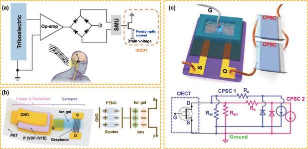
Figure 10. Self-powered neuromorphic systems. (a) Circuit diagram of the auditory nervous system where a triboelectric nanogenerator was employed to monitor the sound signal and drive the OECT. [184] John Wiley & Sons. © 2021 Wiley-VCH GmbH. (b) Diagram of self-powered piezoelectric artificial sensory synapse and corresponding circuit for piezoelectric potential and ion-gel coupling effects. [183] John Wiley & Sons. © 2019 WILEY-VCH Verlag GmbH & Co. KGaA, Weinheim. (c) Schematic diagram of self-powered OECT with two series-connected perovskite solar cells integrated and its corresponding circuit diagram. [184] John Wiley & Sons. © 2021 Wiley-VCH GmbH.
Download figure:
Standard image High-resolution image5.3. Bioinspired nervous systems
The human brain, with its impressive 86 billion neurons, is capable of receiving and collecting signals from a wide range of external stimuli such as sight, touch, hearing, smell, and taste, and then transmitting the relevant information to specific areas within the complex network of the nervous system. The harmonious interplay and intricate interconnection of neural signals within neural networks beautifully pave the way for the emergence of exalted cognitive capacities. These remarkable processes encompass an array of awe-inspiring mental faculties, including the seamless integration of information, recognition, recognition, reasoning and imagination Drawing inspiration from the intricate nervous systems found in biological organisms, it is of paramount importance to develop and execute proficient neuromorphic devices while possessing a comprehensive comprehension of biological neurons, synapses, and brain functionalities [186–190]. Therefore, the integration of various sensors with OECT-based synaptic devices have been explored as artificial neuromorphic systems. Such platforms not only sense various stimuli from surrounding environment, but also perform functions such as perception, learning, memory, computation, and feedback.
For instance, Shim et al developed remarkable OECT synapses through elastomer materials, and such synapses yielded various synaptic behaviors (figure 11(a)) [191]. Even when stretched by 50%, the rubbery synapse still retains all of its performance. A deformable sensory skin was further developed by integrating stretchable OECT with mechanoreceptors in the form of arrays in which mechanoreceptors are connected to external stimuli and generate presynaptic pulses, followed by in-depth demonstrates neurobot that can perform adaptive robot stored in a programmable manner during physical tapping of the skin. Lee et al reported stretchable optoelectronic sensorimotor systems via using organic optoelectronic synapse, where single-wall CNTs and FT4-DPP nanowires were used as electrodes and redox active channel [187]. In this system (figure 11(b)), self-powered photodetector sense external optical signals and generate voltage pulses. Then these pulses drive the stretchable OECT synapses, and the postsynaptic currents are formed. Besides wireless optical communication, this system can serve as artificial muscle actuators that operate in the same manner as biological muscle fibers. This combination of optics, electronics, and biological technology provides promising strategies for the development of next-generation biomimetic neurosoftware electronic [192]. In addition to optoelectronic system, an artificial olfactory system capable of mimicking sense, filtration, learning, and forgetting functions has also been gradually demonstrated. For instance, Chouhdry et al have introduced an artificial chemosensory neuronal synapse, drawing inspiration from the intricate neuronal network discovered within the glomerulus of the olfactory bulb [193]. The proposed system detects chemical stimuli and emulates the functions of inhibitory and excitatory synapses among olfactory receptor neurons, projection neurons, and interneurons (figure 11(c)). The device employs a flexible OECT that is controlled by the potential generated through the interaction of gas molecules (NO2) with ions in a chemoreceptive ionogel. Essentially, this system has the capability to replicate the synaptic functions of chemical synapses in the olfactory system, thereby facilitating the progress of artificial neuronal systems in bionic chemosensory domains.

Figure 11. Flexible OECTs for biological nervous systems. (a) Deformable sensory skin developed by integrating stretchable OECT with mechanoreceptors in the form of arrays. Reproduced with permission from [191]. (b) Organic optoelectronic sensorimotor system, utilizing organic optoelectronic synapse alongside with neuromuscular system that relies on stretchable OECTs. Reproduced with permission from [187]. (c) Schematic illustration of the proposed artificial chemosensory synapse, that can be gated via both chemical (NO2) and electrical stimuli. Reproduced from [193], with permission from Springer Nature. (d) A stretchable neuromorphic implant enables the restoration of coordinated and fluid movement in the legs of mice with neurological movement disorders, granting them the ability to kick, walk, or run seamlessly. Reproduced from [188], with permission from Springer Nature.
Download figure:
Standard image High-resolution image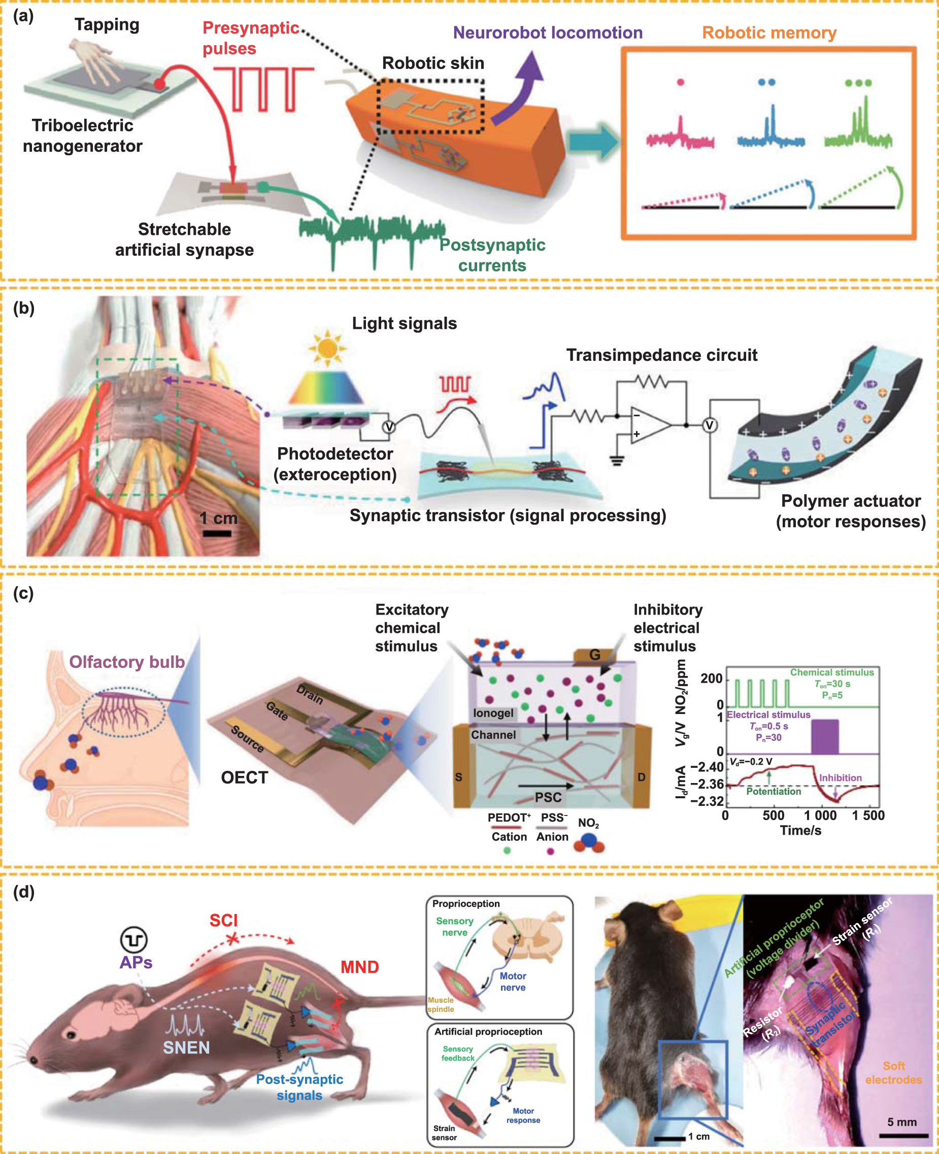
More recently, in addition to using OECT to construct a neurological system with learning functions, OECT-based periprosthetic devices to repair movement in limbs with nerve damage due to spinal cord or lower motor neuron injury have also aroused attention. The concept of the periprosthetic device is to send electrical signals of the nerve form to the muscle as a functional replacement for the damaged nerve by bypassing the injured or damaged nerve in the spine. Lee et al proposed a stretchable OECT neuromorphic efferent nerve that bypasses broken electrophysiological signal pathways and redirects electrophysiological signals that control body movements [188]. It facilitates the restoration of coordinated and smooth movement in mice with neuromotor disorders, allowing them to kick, walk, or run (figure 11(d)). This work paves the way for a novel pathway in neurological repair using OECT. In the future, straightforward systems that harness the principles of neuroplasticity could hold tremendous potential as bioengineering technologies for facilitating voluntary movements in animals with locomotor impairments.
In summary, the design and implementation of efficient neuromorphic devices that mimic the biological nervous system are critically important for the development of next-generation bioelectronics. The integration of various sensors with flexible OECT synapses enable the realization of functions such as sensing, learning, memory, computation, and feedback. Representative examples of such systems are optoelectronic motor systems, artificial olfactory systems, and prosthetic devices for neurological repair (table 5). Hence, the construction of versatile neuromorphic OECTs emerges as a promising avenue towards advancing the development of bioinspired nervous systems, encompassing a wide array of unexplored applications.
Table 5. Summary of bioinspired neuromorphic applications of OECT.
| External sensors | Channel/electrolyte materials of OECTs | Mechanical properties | Synaptic behaviors | Applications | References |
|---|---|---|---|---|---|
| Pressure | P3HT/Ion gel | Stretchable (50%) | EPSC, PPF, STM, LTM | Tactile sensory | [191] |
| Adaptive neurorobotics | |||||
| Pressure | Polymer (P1)/Ion gel | Flexible | EPSC, PPF | Artificial afferent nerve | [181] |
| Pressure | DPPDTSE/Polyelectrolyte | Stretchable (100%) | EPSC, PPF, STP | Biological sensorimotor loop | [194] |
| Temperature | |||||
| Visual | FT4-DPP/Ion gel | Stretchable (100%) | EPSC, PPF | Optoelectronic sensorimotor, muscle actuator | [187] |
| Visual | P3HT/Ion gel | Stretchable (30%) | EPSC | Neuromorphic cognitive functions | [192] |
| Olfactory | PEDOT: PSS/Ion gel | Flexible | EPSC, LTP, LTD | Biomimetic chemosensory | [193] |
| Olfactory | PEDOT: PSS/Ion gel | Flexible | IPSC, PPD, STM, LTM | Biomimetic olfactory | [176] |
| Strain | FT4-DPP/Ion gel | Stretchable (100%) | EPSC, PPF | Proprioceptive feedback | [188] |
| Nerve repair | |||||
| Ion, amino acid, Neurotransmitter | BBL/NaCl | / | Spike | Stimulate biological nerves | [178] |
| Neurotransmitter | PEDOT: PSS/NaCl | / | Spike | Spiking neuron biohybrid interface | [179] |
6. Summary and outlook
Over the past decades, significant advancements in flexible electronics have facilitated the development of OECTs, including material design, novel device architecture, and optimized manufacture technologies. The progress in flexible and stretchable OECTs lead to breakthroughs in the fields of intelligence sensors, human-machine interface, and neuromimetic modulation. Meanwhile, the performance of flexible and stretchable OECT-based systems has reached the level comparable to the rigid counterparts. This progress makes flexible OECTs a considerable candidate for next-generation intelligent bioelectronics. However, there remains a considerable journey ahead to realize these aspirations. Particularly, operation stability, tissue-conformable mechanical properties, manufacturing techniques and bioinspired integration schemes need to be addressed.
- (1)Operational stability: the stability represents the ability to perform reliably during the operation and storage time. Decay in functional materials and external environmental factors (light, heat, and humidity) have negative effect on operational stability. Besides, the continuous electrochemical doping/de-doping process during operation accelerate the functional materials degradation, leading to a short-term stability. So far, most OECT devices have experienced a cycling stability of less than 5000 cycles [13, 73, 195, 196], and such value can be gradually up to 50 000 times through the combination of micro- and nanostructure of the OMIEC material with the newly created vertical device structure [14]. To facilitate the commercialization of OECTs, strategies to design and manufacture OECTs with reliable stability is highly expected. Specifically, materials design and structure engineering can be further introduced to enhance the operational stability, such as manipulating the crystallinity [8, 72, 110, 197, 198], introducing additives to OMIEC film [116, 199, 200], adopting solid-state electrolytes [121, 159, 201, 202], and introducing vertical configuration [14, 90, 203].
- (2)Mechanical properties: OECT-based systems need to be flexible, stretchable, and skin-comfortable, so as to enable good wearability and reliable contact with the tissues. Matching the mechanical properties of soft tissues, such as Young's modulus (1 kPa–10 kPa) and tensile strain (∼30%), is a complex and ongoing research area. Therefore, more flexible device manufacture techniques and material investigations are first desired to optimize the mechanical performance and interfacial adhesion between different device layout components and contact regions, to delve into the details of failure mechanisms for crack analysis during device deformation [204]. In addition, while the 'soft' nature of flexible/stretchable devices may be an opportunity to discover new approaches, these efforts have not yet been fully explored in flexible/stretchable OECT devices, which are mainly used for rigid OECT devices [20]. Nonetheless, the progress in developing low modulus flexible/stretchable material components, such as electrodes, OMIEC materials, and electrolytes, capable of enduring deformation while simultaneously maintaining excellent electrical properties, is highly encouraging.
- (3)Manufacturing techniques: OECT fabrication still faces many challenges, including material incompatibility and poor adhesion between the active layer and flexible substrates. Novel material synthesis and advanced manufacturing techniques are expected to be further explored for reliable and efficient device performances. In addition, scalability and reproducibility are significant obstacles in flexible OECT fabrications. As device fabrication enlarges from lab-scale to commercial-scale, it is essential to offer uniform device performance, high throughput, and low cost. This involves optimizing the fabrication parameters, scaling up the deposition techniques, and establishing quality control measures to ensure batch-to-batch reproducibility. Overcoming these obstacles will pave the way for the widespread adoption of flexible OECTs in various applications, including wearable electronics, and biomedical devices.
- (4)Integration schemes: attention has been paid to expanding flexible OECT devices to intelligent systems owing to their great potential in wearable electronics and bioelectronics. However, most current OECT applications are only available for single functions, such as sensor, or synapse, and there is a dearth of biological nervous system development using OECT as building blocks, which paves a new approach for bionic sensing integration. For example, integration schemes of flexible OECTs with other smart electronics (such as pressure sensors, gas sensors, solar cells, photodetectors, and light-emitting diodes) gradually achieve intelligent electronic systems with multiple advanced functions [99, 139, 160, 205]. Extending its integration with sensors, actuators, and self-powered electronics devices to achieve self-powered, closed-loop, multiple-function artificial sensory and/or neuromorphic systems is also highly expected to open up more possibilities for flexible OECTs. This would promote their commercialization and then significantly change the way humans interact with the world.
Acknowledgments
This work is sponsored by the Regional Joint Fund of the National Science Foundation of China via Grant No. U21A20492, the National Natural Science Foundation of China (NSFC) via Grant No. 62275041, and the Sichuan Science and Technology Program via Grant Nos. 2022YFH0081, 2022YFG0012 and 2022YFG0013, and the Sichuan Youth Software Innovation Project Funding via Grant No. MZGC20230068, and the Sichuan Province Key Laboratory of Display Science and Technology. This work is also supported by City University of Hong Kong (Grant Nos. 9440298 and 9680322) and NSFC via Grant No. 61421002. L Gao also thanks the Academic Support Program for PhD students supported by UESTC.
Conflict of interest
The authors declare no conflict of interest.