
Abstract
Diamond is a highly valuable material with diverse industrial applications, particularly in the fields of semiconductor, optics, and high-power electronics. However, its high hardness and chemical stability make it difficult to realize high-efficiency and ultra-low damage machining of diamond. To address these challenges, several polishing methods have been developed for both single crystal diamond (SCD) and polycrystalline diamond (PCD), including mechanical, chemical, laser, and ion beam processing methods. In this review, the characteristics and application scope of various polishing technologies for SCD and PCD are highlighted. Specifically, various energy beam-based direct and assisted polishing technologies, such as laser polishing, ion beam polishing, plasma-assisted polishing, and laser-assisted polishing, are summarized. The current research progress, material removal mechanism, and influencing factors of each polishing technology are analyzed. Although some of these methods can achieve high material removal rates or reduce surface roughness, no single method can meet all the requirements. Finally, the future development prospects and application directions of different polishing technologies are presented.
Highlights
The existing hurdles and various techniques for polishing diamond are summarized.
Laser, ion beam, plasma-assisted, and laser-assisted polishing methods are reviewed.
Material removal mechanism and influencing factors of various techniques are stated.
Future directions of energy beam polishing techniques for diamond are discussed.
Plasma-assisted polishing is suitable to get high-quality large diamond substrates.
Export citation and abstract BibTeX RIS

Original content from this work may be used under the terms of the Creative Commons Attribution 4.0 license. Any further distribution of this work must maintain attribution to the author(s) and the title of the work, journal citation and DOI.
1. Introduction
Diamond is a remarkable material with numerous desirable properties, including unparalleled hardness, strong wear resistance, high thermal conductivity, and good light transmission [1–3]. Besides, it has a wide band gap of 5.5 eV, high electron mobility of 4500 cm V−1 S−1, and high critical breakdown electric field of 10 MV cm−1 [4, 5]. Due to these exceptional physical and chemical characteristics, diamond is widely used in high-precision cutting tools, optical components, heat dissipation components, and high-power electronics [6–12]. Moreover, among the various common wide band gap semiconductors, diamond is hailed as the ultimate semiconductor, as shown in figure 1. Furthermore, owing to its excellent wear resistance and chemical stability, diamond is considered to be the ideal tool material for nanocutting [13, 14], nanoindentation [15, 16], nanoscratching, etc. With the rapid development of ultra-precision machining and semiconductor technologies, diamond has become one of the most promising materials in modern industry.
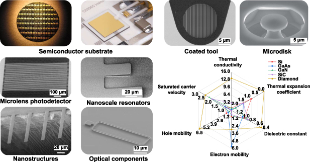
Figure 1. Main applications of diamond [6, 7, 9–12]; performance comparison of main semiconductor materials (for comparison, the properties of silicon are thermal conductivity: 150 W m−1 K−1, thermal expansion coefficient: 2.6 µm m−1 K−1, dielectric constant: 11.8, electron mobility: 1500 cm2 V−1 g−1, hole mobility: 450 cm2 V−1 g−1, and saturated carrier velocity: 105 m s−1). Reprinted from [6], Copyright (2013), with permission from Elsevier. Reproduced with permission from [7]. Reproduced from [9]. © The Author(s). Published by IOP Publishing Ltd CC BY 4.0. Reproduced from [10], with permission from Springer Nature. Reprinted from [11], with the permission of AIP Publishing. [12, 2022], reprinted by permission of the publisher (Taylor & Francis Ltd, www.tandfonline.com).
Download figure:
Standard image High-resolution imageThe high cost and limited availability restrict the practical and industrial applications of natural diamond. However, recent advancements in chemical vapor deposition (CVD) technology have enabled the large-scale production of synthetic diamonds with various sizes and shapes [17, 18]. As a result, high-performance diamond elements can now be used in modern high-technology fields such as nuclear fusion reactors, x-ray optics, biochip substrate and sensors, and nanostructured devices [19–22]. To machine these diamond elements, both high-quality diamonds and sophisticated machining techniques are required for cutting, grinding, and polishing diamond crystals. CVD diamond films have also gained popularity in fields such as cutting tools, semiconductors, and heat sinks [23, 24]. However, the thickness of CVD diamond films is generally non-uniform, and their surface roughness tends to increase with the increase in thickness [25]. Consequently, the development of efficient technologies to resolve these issues in polishing CVD diamond films has received considerable attention. Nonetheless, the high hardness, wear resistance, and chemical inertness of diamond have always been technical challenges in modern manufacturing [26, 27]. Most industrial applications of diamond require high-precision flattening to obtain ultra-smooth and damage-free surfaces. Therefore, the polishing and grinding processes are crucial for the industrial application of diamond. With the continuous development of semiconductor technology and the widespread use of CVD diamond films, the quality of polished diamond surface has improved considerably. Nevertheless, choosing an appropriate polishing technology has emerged as an urgent problem in the diamond processing industry.
The diamond polishing process dates back to 600 years ago, and for centuries, the most common method of polishing diamonds has been to press them onto a rapidly spinning cast iron disc loaded with diamond grit [28]. However, it was not until 1920 that Tolkowsky [29] systematically summarized the diamond polishing process for the first time. With the rapid industrial revolution, diamond grinding and polishing technologies have continuously advanced, and many innovative diamond polishing techniques have been established. Mechanical polishing (MP) [30, 31], chemical–mechanical polishing (CMP) [32, 33], thermochemical polishing (TCP) [34, 35], dynamic friction polishing (DFP) [36, 37], laser polishing (LP) [38, 39], ion beam polishing (IBP) [7, 40], electrical discharge machining (EDM) [41, 42], ultrasonic-assisted polishing (UAP) [43, 44], plasma-assisted polishing (PAP) [45, 46], and laser-assisted polishing (LAP) [47, 48] are some of the commonly used techniques, each with its own advantages and limitations. Among them, MP has simple equipment and low processing costs, DFP has high polishing efficiency, and CMP and TCP have high polishing accuracy.
Although the polishing technology of diamonds has been extensively studied, the conventional polishing techniques like MP, DFP, and CMP can cause varying degrees of damage to the surface, such as scratches, cracks, and subsurface damage [5, 49], which limits the use of single crystal diamond (SCD) substrates in semiconductor and precision optics applications. As shown in figure 2, energy beam-based direct and assisted polishing technologies utilize lasers, ion beams, or plasma to ablate, impact, or modify the diamond surface. Direct polishing technologies include LP, IBP, and EDM. Assisted polishing technologies include PAP and LAP. LP is a non-contact polishing technique that utilizes thermal ablation to graphitize the surface of diamonds, selectively removing protrusions from the diamond surface based on the height difference between surface peaks and valleys [38]. LP integrates the advantages of laser processing to achieve efficient polishing, but it can easily cause thermal defects on the diamond surface. Recent studies have mainly focused on improving the polishing quality by selecting reasonable lasers and adjusting laser parameters and incidence angle. IBP uses high-energy ion beams or clusters to bombard the surface of diamond substrate or film to remove protrusions by graphitization and amorphization [40]. The type and parameters of ion beams can affect the polishing quality of IBP. PAP is a polishing method combining chemical and mechanical material removal, which involves surface chemical reactions induced by plasma. This method not only obtains high-quality surface but also provides high polishing efficiency. PAP has been applied to superhard materials such as diamond, sapphire, and silicon carbide [44, 46]. LAP, which is based on laser-induced chemical reactions, has been successfully applied for the polishing of SCD, polycrystalline diamond (PCD), and CVD diamond films [47]. The main influencing factors of PAP and LAP are the type of plasma or laser, type of reactive gas, material of the polishing disc, and the contact parameters of the polishing interface. The use of energy beam or energy beam-assisted polishing has become the main development trend in the field of diamond polishing. EDM is a spark erosion technique that can create smooth surfaces. However, it is mainly used to process PCD containing metallic bonds, making it difficult to process undoped pure diamonds. Therefore, EDM technology is not widely used for diamond polishing, and this technology is not described in detail here [41, 42].

Figure 2. Energy beam polishing techniques of diamond [8, 39, 46, 48, 50–53]. Reproduced from [8] with permission from the Royal Society of Chemistry. [39] John Wiley & Sons. © 2021 Wiley-VCH GmbH. Reproduced from [46], with permission from Springer Nature. Reprinted from [48], Copyright (2013), with permission from Elsevier. Reprinted from [50], Copyright (2022), with permission from Elsevier. Reprinted from [51], Copyright (2021), with permission from Elsevier. Reprinted from [52], Copyright (2018), with permission from Elsevier. Reprinted from [53], Copyright (2014), with permission from Elsevier.
Download figure:
Standard image High-resolution imageIn this review, the processing characteristics and polishing methods of SCD and PCD are classified and comprehensively analyzed, and the surface polishing technologies suitable for these materials are summarized. Specifically, two types of energy beam-based direct polishing techniques (LP and IBP) and two types of energy beam-assisted polishing techniques (PAP and LAP) are discussed. Furthermore, the technical progress, material removal mechanism, and influencing factors of these polishing technologies are presented.
2. Processing characteristics and polishing methods of SCD and PCD
2.1. SCD
To achieve material surfaces with low roughness and minimal subsurface damage, it is essential to comprehend the material removal and damage generation process during polishing. For SCD, which exhibits significant anisotropy, investigating the deformation mechanism of subsurface dislocations and slip systems can provide valuable insight into the contact machining processes. Recent developments in this area involve indentation and scratching experiments as well as numerical simulations on different crystal planes.
Molecular dynamics (MD) simulations have been extensively employed to systematically explore the nanoindentations on the (001), (110), and (111) planes of SCD [54, 55]. Previous studies have been restricted to an indentation depth of less than 2 nm due to the limited computational ability, and the SCD remained in the elastic stage [56]. However, when the indentation depth reached 4 nm, a pop-in event was observed in the force–displacement (P–h) curve obtained from the MD simulation of nanoindentation on the (001) plane, indicating the onset of plasticity in diamond [55]. Figures 3(a)–(c) illustrate the P–h curves of indentations on the (001), (110) and (111) planes [54]. The P–h curves are highly consistent with the results obtained from the Hertz solution in the elastic stage until the pop-in events occur in all three planes. The results indicate significant differences in the elastic modulus and elastic–plastic critical points in the three crystal planes of SCD. The dislocation structures and distributions of octahedral shear stress under the three planes are shown in figures 3(d)–(f) [54]. The dislocation rings mainly occur along {111}<110>, which is in agreement with the experimental results, and they exhibit significantly different patterns in different planes. The pattern under the (001) plane is fourfold-symmetric, whereas that under the (110) and (111) planes is axisymmetric and threefold-symmetric, respectively [54]. This suggests that the subsurface dislocations and slip deformation generated during the processing of SCD have significant anisotropy.
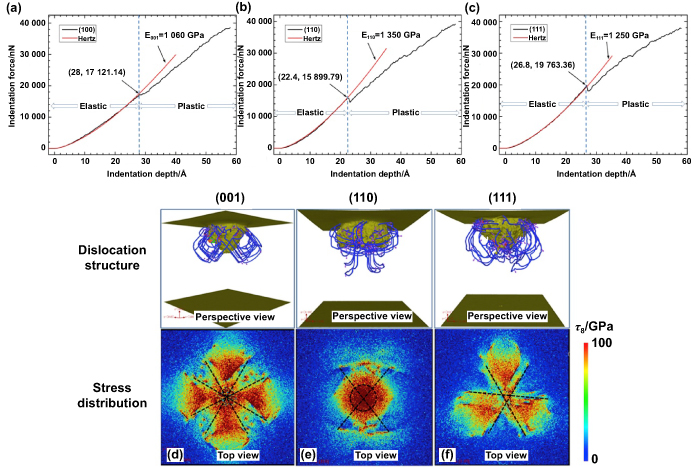
Figure 3. Indentation curve and dislocation analysis on different SCD crystal planes. (a)–(c) Indentation P-h curves on: (a) (001) plane, (b) (110) plane, and (c) (111) plane; (d)–(f) dislocation structures and distributions of octahedral shear stress at the indentation depth of 5.8 nm on (001), (110), and (111) planes [54]. Reprinted from [54], Copyright (2018), with permission from Elsevier.
Download figure:
Standard image High-resolution imageSCD shows obvious anisotropy during processing. There are three principal crystal lattice plane groups in diamond: cubic {100}, dodecahedral {110}, and octahedral {111}. Schuelke and Grotjohn [6] summarized the anisotropic regularity during SCD processing, as shown in figures 4(a)–(c). Even for the same crystal plane, there are harder or softer polishing directions. For example, the <100> direction, along which a higher removal rate and better surface quality can be obtained, is considered to be a soft direction on the (001) plane, while the <110> direction is a hard one, which should be usually avoided.
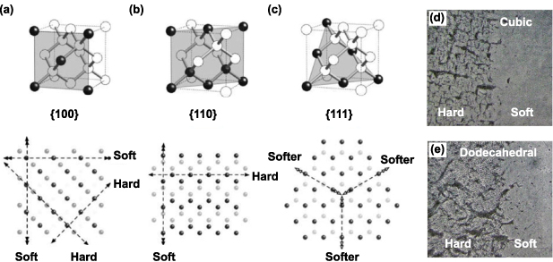
Figure 4. Effect of anisotropy on the polishing quality of SCD. (a)–(c) Diamond crystal anisotropy [6]. Influence of hard and soft polishing directions on the surface of (d) {100} and (e) {110} planes [6]. Reprinted from [6], Copyright (2013), with permission from Elsevier.
Download figure:
Standard image High-resolution imageHird and Field confirmed that the anisotropy of SCD can seriously affect the wear rate during polishing [57]. The final quality of the polished surface is also a function of the wear rate and is therefore anisotropic. Polishing along the soft direction tends to produce a smooth surface, while polishing along the hard direction tends to cause a rougher surface. Figures 4(a)–(c) shows the preferred or soft grinding direction on different SCD facets [6, 58]. Figures 4(d) and (e) show that the direction of hard polishing and soft polishing has a great influence on the finish of {100} and {110} surfaces of SCD [6, 59].
2.2. PCD
PCD is applied in electronic substrates and wear-resistant parts. It can be categorized into PCD tools, PCD substrates, and PCD films. PCD films are usually prepared by CVD, also known as CVD diamond films. PCD films can be classified based on the average grain size as microcrystalline diamond (MCD, >100 nm), nanocrystalline diamond (NCD, 10–100 nm), and ultrananocrystalline diamond (UNCD, <10 nm), as illustrated in figure 5 [58–63]. The process of preparing PCD films involves seeding nano-diamond particles onto a substrate surface and gradually growing them into a thin film via hydrogen-rich chemical reactions in a chamber containing methane and H2 gas [59]. The grain size of the film is affected by the seeding density and environmental pressure of the particles. In general, the production of MCD involves using a very low percentage of CH4 [64], while NCD production requires seeding nanoparticles with a high nucleation density [65]. On the other hand, UNCD is typically grown in environments with a low hydrogen concentration and a high argon concentration [66]. Figure 5 illustrates that when prepared using the CVD method, the MCD film exhibits the highest surface roughness, followed by the NCD film, while the UNCD film shows the best surface quality, achieving a root-mean-square (RMS) roughness value of 5 nm [2].
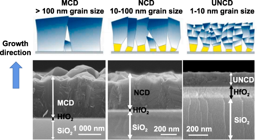
Figure 5. Schematic diagram and cross-sectional scanning electron microscopy (SEM) images of different diamond phases (MCD, NCD, and UNCD) deposited on silicon substrate [63]. Reprinted from [63], Copyright (2022), with permission from Elsevier.
Download figure:
Standard image High-resolution imagePCD films are commonly used in coating tools [67], ultra-precision machining [57], and electronic devices [68]. However, during the growth process of PCD thin films, defects such as asymmetric thickness, random crystal orientation, and uneven crystal grains frequently occur [63]. These defects lead to a rough surface, which limits the industrial applications of PCD films [69]. Bhat et al [70] reported that the roughness of CVD diamond film on the surface of coated tools greatly impacts the cutting efficiency, machining accuracy, and final surface quality. Similarly, Yang et al [69] pointed out that the roughness of PCD films on the surface of high-power electronic components significantly affects their heat dissipation efficiency. The heat dissipation efficiency decreases with the increase in roughness. The material removal rate (MRR) differs significantly among different crystal faces on the PCD surface, which is usually exposed to a large number of such faces. Malshe et al [71] explained that the competitive growth of adjacent crystals during CVD to produce PCD forms micro-cavities that severely limit the high-precision surface polishing. Hence, traditional MP technology is ineffective for PCD surfaces.
2.3. Polishing method
Table 1 summarizes the properties of different polishing methods for SCD and PCD. The anisotropy of SCD is the main factor affecting its polishing quality. Several mechanical, chemical, laser, and ion beam processing methods have been developed for polishing SCD. These methods can be categorized into two groups: ordinary polishing technology and mixed polishing technology. Ordinary polishing technology utilizes a single material removal method, including MP, TCP, DFP, LP, and IBP. By contrast, mixed polishing technology involves the use of multiple material removal methods, such as CMP, PAP, LAP, and UAP.
Table 1. Characteristics and polishing methods of SCD and PCD.
| Diamond | SCD | PCD | ||
|---|---|---|---|---|
| Classification | HPHT CVD | CVD diamond films (PCD films) | PCD substrates | PCD tools |
| Properties | High thermal conductivity, high light transmittance, high chemical stability, and good semiconductor performance | Low friction coefficient, high adhesion, high wear resistance, and good thermal conductivity | Good thermal conductivity | High hardness, high wear resistance, low coefficient of thermal expansion |
| Difficulties in polishing | The anisotropy of SCD can seriously affect the wear rate and surface finish during polishing | Uneven thickness, uneven grain size, uneven surface | The removal rates of different crystal orientations on the surface of PCD differ significantly | The edges and some curved surfaces of PCD tools are difficult to polish |
| Conventional polishing techniques | MP, CMP, TCP, DFP, UAP | CMP, TCP, DFP, UAP | ||
| Deficiencies of conventional polishing technology | Scratches, pits, sub surface damage | Microcracks, surface residual stress, breakage | Scratches, cracks, low accuracy | Unable to polish precision edges |
| Can only be used for planar polishing, unable to polish curved surfaces | ||||
| Energy beam polishing technology | LP, IBP, PAP, LAP | LP, IBP, EDM, LAP | ||
The difference in crystal orientation and uneven grain size on the surface of PCD as well as the uneven thickness of CVD diamond films can cause great difficulties in polishing PCD. Therefore, the polishing difficulty of PCD is generally higher than that of SCD. Currently, there are several technologies for polishing the surface of PCD. Conventional polishing techniques include CMP, TCP, DFP, and UAP. Energy beam polishing techniques include LP, IBP, and LAP. Non-contact polishing technologies like LP and IBP can be used to polish various plane and curved surfaces and are currently the most commonly used polishing technologies for CVD diamond films. All these technologies, except EDM, can be used for the surface polishing of both SCD and PCD.
As shown in table 1, the conventional polishing techniques can cause some defects on the diamond surface [3, 66]. Although CMP technology has high accuracy, its MRR is too low. In addition, conventional polishing techniques cannot be used for curved surface polishing, which limits their application in the preparation of precision diamond components. Energy beam polishing technology can make up for the shortcomings of conventional polishing technology and are expected to become a research hotspot in the field of diamond polishing.
2.4. Characteristics and limitations of conventional polishing techniques
Table 2 summarizes the characteristics of various conventional diamond polishing techniques. These techniques are classified based on several aspects, including the processing mechanism, polishing quality, polishing efficiency, equipment cost, and commercial application. MP, DFP, and UAP are room-temperature polishing techniques that do not usually involve sample heating [30, 36, 43]. On the other hand, TCP and CMP typically require heating modules to elevate the temperature of the contact interface, enabling effective material removal [6, 72, 73].
Table 2. Summary of characteristics of conventional polishing techniques.
| Polishing method | MP | TCP | CMP | DFP | UAP |
|---|---|---|---|---|---|
| Temperature | Room | >750 °C | >300 °C | Room | Room |
| Mechanism | Microdissociation | Phase change, hot metal plate, thermal diffusion etching | Oxidation, abrasion | Phase change, abrasion and chemical reaction caused by friction heating | Microdissociation caused by ultrasound, abrasion and micro cleavage |
| MRR | Polishing plate: <0.5 μm h−1; (0.253 μm h−1 [82]) | SCD: <1 μm h−1 (0.15 μm h−1 [89]) | <1 μm h−1 (0.5 μm h−1 [78], 0.37 μm h−1 [79]) | >200 μm h−1 (222 μm h−1 [36]) | 50–200 μm h−1 |
| SCD: 45 μm h−1 [43], | |||||
| PCD: 200 μm h−1 [75] | |||||
| Grinding wheel: >50 μm h−1 (56.35 μm h−1 [80]) | PCD: 5–10 μm h−1 (9.6 μm h−1 [73]) | ||||
| Surface quality | Polishing plate: Ra 1–10 nm (Ra 1.66 nm [82], Ra 1.65 nm [83]) | SCD: Ra < 0.5 nm (Ra 0.16 nm [85]) | SCD: Ra 0.5–5 nm (Ra 0.82 nm [84], Ra 1.66 nm [91]) | Ra 20–500 nm | SCD: Ra 10 nm [92], |
| Grinding wheel: Ra 0.5–2.5 µm (Ra 0.55 μm [86] Ra 2.5 μm [80]) | PCD: Ra 25 nm [73] | PCD: Ra 0.1–1.5 µm (Ra 20 nm [93], Ra 95 nm [73]) | (Ra 20 nm [81], Ra 397 nm [36]) | PCD: Ra 0.5 µm [75] | |
| Cost | Low | High | High | High | High |
| Advantages | Low cost, simple equipment | High polishing accuracy, high material removal rate (MRR) | High polishing accuracy | High MRR, low cost | High MRR |
| Disadvantages | Low polishing accuracy, easy to cause mechanical damage | Complex equipment, high cost, thermal damage | Complex equipment, high cost, and low MRR | Low polishing accuracy, with defects on the polished surface | Complex equipment, low polishing accuracy |
| Main limitations | Can only be used for planar polishing, unable to polish curved surfaces, unable to balance polishing accuracy and MRR, unable to achieve precision polishing of large-sized diamond substrates | ||||
The material removal mechanism of diamond can be categorized into six types: abrasion and micro cleavage, carbon structure transformation, diffusion, chemical reaction, evaporation, and sputtering [28]. A diamond polishing technology typically involves a combination of these material removal mechanisms. MP and UAP primarily rely on abrasion and micro cleavage for material removal [74, 75]. TCP combines chemical reaction, diffusion, and evaporation for material removal [35]. CMP utilizes chemical reaction, abrasion, and evaporation as the material removal mechanisms [76]. DFP involves abrasion, carbon structure transformation, diffusion, and evaporation for material removal [77].
DFP and UAP exhibit the highest MRRs, typically ranging from tens to hundreds of microns per hour [36, 43, 58]. TCP follows with a medium MRR, typically up to 10 μm h−1 [69]. CMP has the lowest MRR, usually less than 1 μm h−1 [78, 79]. Generally, MP has lower efficiency, but recent advancements in the grinding wheel technology such as the use of various metallic materials and the introduction of ultrasonic-assisted processes have significantly improved its efficiency. MP can now achieve MRRs up to tens of microns per hour [80]. Nevertheless, it is important to note that the surface precision obtained by polishing with grinding wheel remains limited.
In general, the polishing techniques with high MRRs have limitations in achieving high-quality surfaces. For instance, DFP can cause mechanical damage to the diamond surface and is typically suitable for processing surfaces with roughness in the range of tens of nanometers [36, 81]. On the other hand, MP can achieve surface roughness in the range of several nanometers [82, 83]. CMP is capable of producing sub-nanometer precision surfaces with a roughness (Ra) below 1 nm [84]. TCP, being a precision polishing technique, can achieve ultra-high precision surfaces with roughness below 0.5 nm [85]. Due to the random crystal orientation distribution and grain inhomogeneity, CVD diamond films often have an initial roughness of several microns, which is significantly larger than that of SCD surfaces. Diamond films are usually polished by CMP, DFP, and UAP. The surface roughness of polished diamond films can reach tens to hundreds of nanometers [73, 75, 86].
MP is the most widely used diamond polishing technique due to its simple equipment and low cost [87, 88]. The cost of CMP is higher than that of MP, and it is widely used for precision polishing of diamond substrates [81]. The cost of TCP is slightly higher than that of CMP due to the incorporation of heating equipment [89]. DFP and UAP are commonly used for efficient polishing of SCD substrates and CVD diamond films due to their excellent polishing efficiency [75, 90]. The cost of DFP and UAP is high due to the high manufacturing cost of alloy polishing plate and the introduction of ultrasonic equipment.
According to table 2, it is evident that conventional polishing methods have their own advantages and disadvantages. In general, these methods have certain limitations that need to be considered. These limitations include their suitability for flat polishing only, inability to polish curved surfaces, difficulty in balancing polishing accuracy with MRR, and the challenge in achieving precision polishing for large-sized diamond substrates. These limitations make it difficult to produce ultra-precision diamond components and substrates. Therefore, it is crucial to explore new energy beam polishing technologies for boosting the industrial application of diamonds in various fields.
3. Progress of energy beam-based direct and assisted polishing techniques for diamond
3.1. LP
LP, a non-contact and pressureless polishing process, is primarily used for polishing diamond films, diamond tools, and drill truing. In 1987, Rothschild et al [94] first reported the LP technology for polishing diamond. In 1999, Pimenov et al [95] used a copper vapor laser (510 nm wavelength) to polish 150–400 μm thick diamond films and discovered that the surface roughness was dependent on the incidence angle of the laser beam and the polishing time. In 2017, Wang et al [96] achieved a RMS roughness of 1.299 μm on a 250 μm thick CVD diamond film using a 248 nm pulsed excimer laser. Their results indicated that the surface roughness of the polished diamond decreased with the decrease in incidence angle, and the polishing rate increased logarithmically with the increase in laser flux.
Over the recent years, there has been a growing demand for improving the surface quality of diamond substrates due to their wide applications in the semiconductor and optical fields. The polishing quality and efficiency of LP have been improved by experimenting with different laser types, adjusting laser parameters, and using surface absorption films. Ogawa et al [97] found that the roughness of PCD surface processed by femtosecond laser was significantly better than that processed by nanosecond laser. Kononenko et al [98] covered the surface of PCD with thin absorption films (metal, graphite) and polished the surface with a wide-pulse infrared laser (10 ns). The results showed that the absorption film significantly reduced the ablation threshold and the polished surface roughness of diamond. Scalbert et al [99] developed a high-power femtosecond laser ablation process to achieve high-throughput polishing of PCD wafers, with an MRR twice that of MP when polishing the surface of fine-grained diamond, and the surface roughness was also significantly reduced. Cui et al [100] studied the influence of laser intensity on the polishing quality of CVD diamond films achieved by femtosecond LP, and the best laser intensity was found to be 0.7 J cm−2. Liu et al [39] developed a nanosecond LP device with a wavelength of 355 nm to polish the surface of SCD substrate, as shown in figure 6. Nanosecond LP of diamond mainly includes two processes: graphitization of diamond surface by high-energy laser beam irradiation and removal of graphite layer by ablation. Figure 6(c) shows a schematic of the laser ablation of diamond. It can be seen that the ablation threshold and graphitization threshold affect the ablation depth. Therefore, during the LP process, the ablation depth should be reasonably controlled by adjusting the laser energy. As shown in figures 6(d)–(f), after 40 ns laser scans, the surface roughness (Ra) of diamond decreases from 336.2 nm to 8.02 nm.
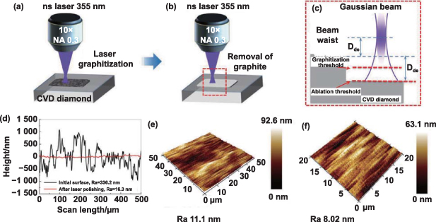
Figure 6. Principle and effect of laser polishing (LP) on CVD single crystal diamond using a femtosecond laser: (a) laser graphitization, (b) laser ablation of the graphitized layer by 355 nm nanosecond laser, (c) illustration of defocusing configuration of Gaussian beam (Dde: amount of laser defocusing, Dab: ablation depth), (d) comparison of surface profiles before and after LP, (e) and (f) atomic force microscopy (AFM) morphology of polished surface. [39] John Wiley & Sons. © 2021 Wiley-VCH GmbH.
Download figure:
Standard image High-resolution imageTable 3 summarizes some recent research results on the LP of diamond, mainly including the polishing quality, polishing efficiency, and laser parameters used. It can be seen that there is a significant difference between the polishing qualities of diamond films and SCD substrates. The minimum RMS roughness of polished diamond films can only reach 31.88 nm, while the surface roughness (Ra) of SCD substrates can reach 8.02 nm.
Table 3. Main achievements in laser polishing (LP) of diamond.
| Diamond | Initial roughness | Final roughness | Laser type | Laser frequency | Laser wavelength | Energy density | Removal rate | References |
|---|---|---|---|---|---|---|---|---|
| CVD diamond film | Ra 3.4 μm | Ra 0.59 μm | Copper vapor laser | 15 kHz | 510 nm | 6.5 J·cm−2 | — | [95] |
| CVD diamond film | RMS 3.314 μm | RMS 1.299 μm | KrF excimer laser | 20 Hz | 248 nm | 3.48 J·cm−2 | 24.19 μm h−1 | [96] |
| CVD diamond coating | Ra 1.85 μm | Ra 0.51 μm | Picosecond laser | 200 kHz | 515 nm | 1.81 J·cm−2 | — | [101] |
| NCD film | RMS 73.84 nm | RMS 31.88 nm | Femtosecond laser | 50 MHz | 1040 nm | 0.7 J cm−2 | — | [97] |
| SCD substrate | Ra 336.2 nm | Ra 8.02 nm | Nanosecond laser | 50 kHz | 355 nm | 3.53 J cm−2 | — | [39] |
3.2. IBP
In 1972, Spencer and Schmidt [102] machined a hole with a diameter of 0.375 mm on the surface of a diamond substrate using an Ar ion beam and polished the inner surface of the hole. In 1990, Hoffman et al [103] studied the graphitization phenomenon that occurs when 1.5 keV argon and hydrogen ions bombard the (100) surface of diamond. In 1992, Grogan et al [104] polished a CVD diamond film with a 500 eV oxygen ion beam, reducing the RMS surface roughness of the film from 1.26 μm to 35 nm. In 1996, Vivensang et al [105] reported a method based on reactive ion etching (RIE) technology to reduce the surface roughness of CVD diamond films to 14 nm. In 2000, Koslowski et al [106] bombarded the (100) surface of diamond with low-energy (1.2–1.5 keV) Ar+ ions, achieving a minimum RMS roughness of only 0.1 nm. In 2019, Mi et al [107] used an Ar+ ion beam (700 eV, 1.1 mA cm−2, incidence angle: 60°) to polish the SCD substrate with scratches. As shown in figures 7(a)–(c), after 20 min of polishing, the trench depth on the substrate surface has decreased from 108 nm to 8 nm.
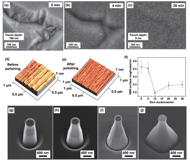
Figure 7. Effect of IBP treatment on diamond. SEM image of a single trench (a) before, (b) after 4 min and (c) after 20 min of Ar+ ion beam polishing [107]. Reprinted from [107], Copyright (2019), with permission from Elsevier. AFM images of the HPHT diamond (d) before polishing and (e) after polishing by ICP Ar/Cl2 plasma for 10 min; (f) variation in the surface roughness with ICP time [108]. Reprinted from [108], Copyright (2008), with permission from Elsevier. SEM images of monolithic diamond nanopillars: (g) 3.4°, (h) 7.5°, (i) 11.5°, and (j) 21°. [112] John Wiley & Sons. © 2018 WILEY-VCH Verlag GmbH & Co. KGaA, Weinheim.
Download figure:
Standard image High-resolution imageIn the 21st century, numerous ion-based diamond processing technologies have emerged due to the rapid development of ion generation equipment, such as ion beam etching (IBE), RIE, ion beam assisted chemical etching (IBAE), and reactive ion beam assisted chemical etching (RIBAE). In addition, inductively coupled plasma (ICP), electron cyclotron resonance (ECR) plasma, and focused ion beam (FIB) have been successfully used for ultra-precision machining of diamonds [108]. Schmitt et al [109] investigated the ability of IBE to polish defined rough areas after RIE processing. They studied the effects of an oxygen–argon mixture and etching depth on the surface quality of nano diamond films produced by RIE processing. The results showed that the surface roughness increased with the increase in oxygen content and etching depth but decreased with the increase in argon content. Schmitt et al confirmed that the polishing efficiency of combining IBE and RIE is four times higher than that of only IBE. Harker et al [110] polished a rough PCD film with an iron plate under the action of active oxygen and hydrogen ion beam and obtained a high-quality surface with Ra below 10 nm. Nagai et al [35] studied the ability, etching efficiency, and quality of various ion beam technologies to etch SCD. The results showed that RIBAE had the highest etching efficiency and caused the least damage to the diamond crystal structure. Ieshkin et al [111] studied the influence of accelerated gas cluster ion bombardment on the surface morphology of SCD. The 10 keV gas cluster ions with a total dose of more than 1016 cm−2 could produce a high-quality surface with an RMS roughness of 1.62 nm. Lee et al [108] studied the effect of ICP on the surface of high-pressure, high-temperature (HPHT) diamond. As shown in figures 7(d)–(f), after 10 min of ICP treatment, the RMS surface roughness of diamond surface decreases from 0.53 nm to 0.19 nm. This indicates that ICP can produce very smooth diamond surfaces with high polishing efficiency.
Recently, RIE has emerged as a promising method for diamond polishing. The MRR of RIE method for diamond with O2 and H2 has been found to be 2.1 μm h−1, which is three times higher than that of IBP [113]. Further, RIE results in better surface quality of diamond. It has been reported that the crystalline structure of diamond after reactive ion processing is preserved and no obvious damage is detected, while an amorphous layer with a thickness of 11 nm and sp2 structures are found on the diamond surface after FIB processing [114]. Hicks et al [115] achieved near-zero density of surface pits using the Ar/O2/CF4 reactive plasma etching, and the addition of argon made a significant contribution, reducing the surface roughness by 20%–44%. Zheng et al [50] used microwave hydrogen plasma to treat the surface of SCD and obtained a high-quality surface with an RMS surface roughness of 4.2 nm. The MRR of this technology is 169 nm h−1. In recent years, RIE has been used for the nano-structuring and nano-patterning of SCD. For example, Xie et al [112] compared the etching of different crystal faces of diamond and proposed a dry etching principle based on crystal direction. According to this principle, the monolithic diamond nanopillars for magnetometry have been fabricated, as shown in figures 7(d)–(g). The half-tapering angle of these nanopillars can reach 21°, which implies high photon efficiency and high mechanical strength.
Table 4 summarizes the recent research achievements content of IBP on diamonds, mainly including polishing quality, MRR, types of ion beams, and parameters of ion beams. The effects of IBP on CVD diamond films and SCD substrates are significantly different. The minimum surface roughness (Ra) of CVD diamond films obtained by IBP can reach 14 nm, and the MRR can reach 1.8 μm h−1. The minimum RMS surface roughness of SCD substrate obtained by IBP can reach 0.1 nm, and the MRR can reach 169 nm h−1.
Table 4. Main research achievements of ion beam polishing (IBP) on diamond.
| Diamond | Initial roughness | Final roughness | Type of ion beams | Energy/Chamber pressure | Current density/Power | Removal rate | References |
|---|---|---|---|---|---|---|---|
| CVD diamond film | RMS 1.26 μm | RMS 35 nm | Oxygen ions | 500 eV | 0.2 mA·cm−2 | 0.82 μm h−1 | [104] |
| CVD diamond film | Ra 40 nm | Ra 14 nm | SF6-O2 plasma | 13.3 Pa | 300 W | 1.8 μm h−1 | [105] |
| PCD-coated tool | Ra 40 nm | Ra 20 nm | Ar+-ion | 1 keV | 0.5 mA·cm−2 | — | [116] |
| SCD substrate | RMS 4.5 nm | RMS 0.1 nm | Ar+-ion | 1.2–1.5 keV | 30 μA·cm−2 | 12 nm h−1 | [106] |
| SCD substrate | RMS 3.23 nm | RMS 1.62 nm | Gas-Cluster ion beams | 10 keV | — | 16 nm per 1016 ion cm−2 | [111] |
| HPHT SCD | RMS 0.53 nm | RMS 0.19 nm | ICP Ar/Cl2 plasma | 0.665 Pa | 400 W | 3.0 μm h−1 | [108] |
| SCD substrate | RMS 1.21 nm | RMS 0.1 nm | Ar+-ion | 1 keV | — | — | [117] |
| SCD substrate | RMS 13.4 nm | RMS 4.2 nm | Hydrogen plasma | 20–21 kPa | 3.9–4 kW | 169 nm h−1 | [114] |
3.3. PAP
In 2011, Yamamura et al [118] proposed the PAP method for SCD surfaces. Liu et al [119] fabricated a device for PAP of SCD, as shown in figures 8(a) and (b). The device creates Ar-based plasma through the radio frequency electric field between the upper electrode and the lower rotating disc and polishes diamond through the chemical and mechanical action between the polishing disc and the substrate under the assistance of plasma. As shown in figure 8(c), the minimum surface roughness Sq of the SCD (100) substrate polished by this device can reach 0.32 nm. To demonstrate that PAP is a nondestructive polishing technology, Liu et al [120] detected subsurface damage of SCD (100) substrates after MP and PAP through scanning cathodoluminescence (CL) with band A emission (central wavelength = 432 nm). Band A emission is considered to be caused by dislocation, sp2 hybrid structure, and other internal damage in diamond [121, 122]. The results showed that there were obvious high luminous intensity scratches on the SCD substrate after MP, but no such scratches were observed after PAP. Luo et al obtained the cross-sectional transmission electron microscopy (TEM) images of SCD in <110> crystal orientation after MP and PAP, which are shown in figures 8(d)–(g) [51]. It can be observed that there is a 3.9 nm thick amorphous layer between the Pt film and the diamond surface after MP, which contains a large number of dislocations. The diamond surface after PAP has no amorphous layer and dislocations. This indicates that PAP has an atomic-level material removal mechanism and can achieve non-destructive processing of diamonds.
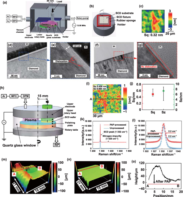
Figure 8. Equipment and polishing effect of PAP on diamond. (a) Experimental setup of the vacuum PAP device; (b) fixing method of SCD substrate; (c) scanning white light interferometric (SWLI) image of SCD substrate surface after PAP [119]. Reprinted from [119], Copyright (2022), with permission from Elsevier. (d)–(g) cross-sectional transmission electron microscopy (TEM) images of SCD in the <110> crystal direction after MP and PAP: (d) and (e) MP, (f) and (g) PAP [51]. Reprinted from [51], Copyright (2021), with permission from Elsevier. (h) Schematic of the experimental setup; (i) SWLI image of one local area on the mosaic SCD (100) substrate after PAP; (j) average and distribution of Sq and Sz values of seven different local areas on the mosaic SCD (100) substrate after PAP obtained by SWLI (84 μm2); (k) micro-Raman spectra of one group of points; (l) magnified Raman lines shown in (k) [46, 123]. Reprinted from [123], Copyright (2018), with permission from Elsevier. (m) SWLI image of the entire mosaic SCD substrate before PAP obtained by the stitching application; (n) SWLI image of the entire mosaic SCD substrate after PAP obtained by the stitching application; (o) cross-sectional profiles of the same point on the mosaic SCD substrate before and after PAP [46]. Reproduced from [46], with permission from Springer Nature.
Download figure:
Standard image High-resolution imageLiu and Yamamura et al [46, 123] used an oxygen-argon-based plasma containing water vapor to modify the surface of a quartz glass polishing plate and achieved a high MRR of 13.3 μm h−1 when polishing SCD (100) substrate. As shown in figure 8(i), the surface roughness Sq after PAP is 0.458 nm, and the maximum surface height Sz is 8.884 nm. The diamond surface after PAP does not show scratches, consistent with the <100> crystal direction, which indicates that anisotropy does not affect the quality of PAP-processed diamond, as shown in figure 8(j). The Raman spectra in figures 8(k) and (l) indicate that there is no non-diamond structure or residual stress on the polished diamond surface. Thus, PAP is a high-quality, nondestructive, and efficient polishing method of diamond. As shown in figure 8(m), the SCD (100) substrate polished by Liu et al [46] has a large size of 21 mm × 19 mm × 1 mm. Based on figures 8(m)–(o), it can be inferred that the large waviness (height ⩾ 100 μm) on the SCD substrate before polishing is completely removed by PAP, and the surface smoothness of the polished substrate is very high. This indicates that PAP technology offers significant advantages in polishing large-sized diamond substrates, with high MRR and polishing accuracy.
Table 5 summarizes the processing parameters and polishing effects of PAP on diamond. Currently, PAP is only successfully used for polishing SCD substrates. In [46, 51, 119, 120], Ar-based oxygen plasma was selected for the PAP of diamond. The polishing accuracy of PAP is extremely high, and the surface roughness Sq of the polished SCD surface is below 0.5 nm, with a maximum MRR of 13.3 μm h−1. In addition, in [46, 120], the SCD substrate had a large size of 20 mm2, indicating that PAP technology has been successfully used for precision polishing of large-sized diamond substrates.
Table 5. Main achievements of plasma-assisted polishing (PAP) for diamond.
| Diamond | Diamond size | Initial roughness | Final roughness | Plasma type | Sliding speed | Polishing pressure | Material removal rate | References |
|---|---|---|---|---|---|---|---|---|
| SCD substrate | 8 × 8 × 1 mm | — | Sq 0.32 nm | Ar-based oxygen plasma | 1.1 m s−1 | 246.9 kPa | 5.3 μm h−1 | [119] |
| SCD substrate | 19 × 21 × 0.5 mm | Sq 7.15 nm | Sq 0.48 nm | Ar-based oxygen plasma | 1.4 m s−1 | 37.59 kPa | 0.55 μm h−1 | [120] |
| SCD substrate | 4 × 4 × 2 mm | Sq 308 nm | Sq 0.86 nm | Inductively coupled plasma (Ar gas and H2O2) | 1.5 m s−1 | 62.5 kPa | 1.5 μm h−1 | [51] |
| SCD substrate | 21 × 19 × 1 mm | Sq 0.66 μm | Sq 0.46 nm | Argon-based oxygen plasma | 1.2 m s−1 | 401 kPa | 13.3 μm h−1 | [46] |
3.4. LAP
In 2009, Anan et al [47] proposed the LAP technology based on the ultraviolet (UV) laser-induced chemical reactions to produce active substances. By polishing the SCD (100) substrate using this technology, the surface roughness Ra decreased from 1.35 nm to 0.19 nm within 120 min of UV laser irradiation. The surface roughness Ra could only reach 0.74 nm without UV laser irradiation.
In 2013, Watanabe et al [48] used a LAP device, as shown in figures 9(a) and (d), to polish both SCD and PCD. The top of the diamond substrate in the device was oxidized and removed under local high temperature. As shown in figures 9(b) and (c), the surface roughness Ra of SCD after polishing under UV laser irradiation can reach 0.19 nm, and the MRR is 0.5 μm h−1. Without UV laser irradiation, the surface roughness Ra of SCD can only reach 0.63 nm, and the MRR is only 0.3 μm h−1. As shown in figures 9(e) and (f), after 180 min of polishing, the diamond tool forms a sharp edge with a half diameter of 0.3 µm. The results suggest that LAP technology can be used for manufacturing ultra-precision tools. In 2018, Kubota and Takita [52] proposed a 172 nm vacuum-ultraviolet (VUV) LAP method, as shown in figure 9(g). This technology uses a laser-modified sapphire polishing plate to polish the SCD substrate. The results show that the MRR under UV laser irradiation (238.1 nm h−1) is about seven times that without UV laser irradiation/(33.3 nm h−1). As shown in figures 9(h) and (i), the surface roughness Ra of diamond decreases from 4.673 nm to 0.133 nm within 1.5 h of irradiation.
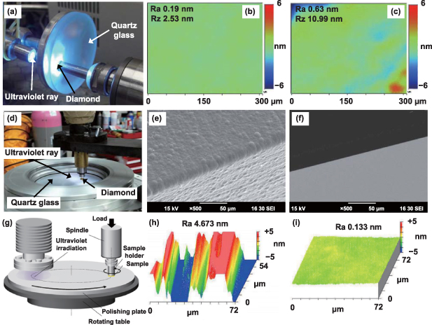
Figure 9. Equipment and polishing effect of LAP on diamond. (a) Horizontal type UV polishing machine for SCD; (b) and (c) SWLI images of SCD (100) substrate after 40 min of UV LP: (b) polishing under UV irradiation, (c) polishing without UV laser; (d) vertical type UV polishing machine for PCD; (e) SEM image of CVD diamond film; (f) SEM image of CVD diamond film edge-sharpened by UV LP for 180 min [48]. Reprinted from [48], Copyright (2013), with permission from Elsevier. (g) Schematic of vacuum-UV (VUV)-assisted polishing apparatus, (h) pre-polished diamond surface, (i) diamond surface polished by VUV laser irradiation [52]. Reprinted from [52], Copyright (2018), with permission from Elsevier.
Download figure:
Standard image High-resolution imageLP has high efficiency, while PAP has high accuracy. Recently, Liu et al [124] proposed an efficient and high-precision polishing process by combining nanosecond laser trimming with PAP. As shown in figures 10(a) and (b), a layer of Cu film is first coated on the surface of the diamond to reduce the graphitization threshold of the diamond. This prevents the high-energy laser beam from burning deep pits on the diamond surface. As shown in figure 10(c), the peak-to-valley value of diamond surface decreases by nearly 70 μm after nanosecond laser treatment. This indicates that laser treatment significantly improves the surface flatness. The G-band in figure 10(d) suggests that there is an obvious graphite layer on the surface of laser- treated diamond. Figures 10(e) and (f) show the topography and Raman spectra of the diamond surface after PAP. The roughness Sq of the diamond surface after PAP reaches 0.51 nm. In figure 10(f), no graphite peak is observed, and the N-peak is an intrinsic impurity peak in the diamond sample. This indicates that the graphite layer is removed by the PAP process, and the polished diamond surface has no other damage. In this experiment, the surface roughness Sq of the diamond after laser treatment is 7.81 μm. After 6.5 h of PAP, Sq decreases to 0.51 nm. Overall, the hybrid polishing process provides high polishing accuracy as well as high polishing efficiency.
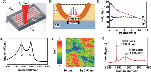
Figure 10. Polishing of SCD substrate by a combination of laser trimming and PAP. (a) Schematic of laser scanning of diamond, (b) schematic of normal vaporization in the laser ablation of Au-coated SCD substrate, (c) cross-sectional profile of the same point on the SCD substrate before and after laser trimming, (d) Raman spectrum of diamond surface after laser scanning, (e) SWLI image of SCD surface after PAP, (f) Raman spectrum of SCD surface after PAP [124]. Reprinted from [124], Copyright (2023), with permission from Elsevier.
Download figure:
Standard image High-resolution imageTable 6 summarizes the polishing effects of LAP on diamonds and the relevant processing parameters. Currently, UV laser (wavelength 200–400 nm) is mainly used for the LAP of diamond. SCD can achieve the highest surface quality by LAP, with a surface roughness Ra of 0.133 nm. However, the MRR of LAP is low. Except for the PCD substrate, the MRR of LAP for diamond is less than 1 μm h−1.
Table 6. Main achievements of LAP for diamond.
| Diamond | Initial roughness Ra | Final roughness Ra | Laser type | Wavelength (nm) | Intensity (mW cm−2) | Polishing pressure (MPa) | Material removal rate | References |
|---|---|---|---|---|---|---|---|---|
| SCD substrate | 1.35 nm | 0.19 nm | UV laser | — | — | 1.0 | 4.71 nm h−1 | [47] |
| SCD substrate | 1.04 nm | 0.21 nm | UV laser | 200–400 | 300 | 1.0 | 0.50 nm h−1 | [48] |
| SCD substrate | 4.673 nm | 0.133 nm | Vacuum UV laser | 172 | 6.0 | 2.2 | 238.1 nm h−1 | [52] |
| CVD diamond film | — | 0.35 nm | UV laser | 172 | 3.4 | — | 0.56 nm h−1 | [48] |
| PCD substrate | 30.0 nm | 5 nm | UV laser | 172 | 3.4 | 1.0 | 2.0 μm h−1 | [48] |
Table 7 presents a summary of various energy beam polishing technologies for diamond, including polishing quality, polishing efficiency, equipment cost, and commercial applications. LP and IBP are widely used non-contact polishing techniques that are not limited by the geometry of the diamond surface. LP and IBP are typically used for polishing CVD diamond films and SCD substrates. PAP and LAP are contact polishing techniques that are limited by the geometry of the diamond surface. LP has the highest MRR, which can be higher than 20 μm h−1. PAP and LAP have the highest polishing quality and can produce high-precision surfaces with Ra below 0.5 nm.
Table 7. Summary of characteristics of various polishing technologies for diamond.
| Technology | LP | IBP | PAP | LAP |
|---|---|---|---|---|
| Contact method | Non-contact | Non-contact | Contact | Contact |
| MRR | >0.001 mm3 s−1, 24.19 μm h−1 | <2 μm h−1 | 1–15 μm h−1 | <2 μm h−1 |
| Surface quality | SCD: Ra 8 nm; | SCD: Ra 0.1–2 nm; | SCD: Ra < 0.5 nm | SCD: Ra < 0.3 nm |
| PCD: Ra 0.03–1.3 µm | PCD: Ra 0.01–1 µm | PCD: Ra 0.3–5 nm | ||
| Cost | Low | High | Very high | Very high |
| Applicable objects | SCD, PCD (CVD diamond film) | SCD, PCD (CVD diamond film) | SCD | SCD, PCD, CVD diamond film |
| Advantages | High MRR, curved surface polishing, low cost | High polishing accuracy, curved surface polishing, microstructure polishing | High accuracy, high MRR, low damage, polishing large-sized diamond substrates | High accuracy, low damage |
| Disadvantages | Low polishing accuracy, thermal damage | High cost, low MRR | High cost, complex equipment | High cost, complex equipment, low MRR |
To recapitulate, LP is a non-contact polishing technology that is not limited by the surface shape of the sample, facilitating flat and curved surface polishing. LP is more efficient than traditional MP and CMP, with a MRR that can reach several nanometers per second. However, the polishing accuracy of LP is limited, and the surface roughness Ra after polishing can only reach 8 nm. Further, the material removal method of thermal ablation can cause thermal cracks and other damage to the diamond surface. Consequently, LP technology is mainly used for polishing CVD diamond films and for surface dressing of diamond tools that are difficult to machine using traditional polishing methods. As a non-contact polishing technology, IBP is not limited by the surface morphology of materials and is suitable for polishing various hard and brittle materials. FIB has been widely used for polishing diamond films, but the MRR is low due to the small size of the ion beam. Higher ion energy may increase the polishing efficiency, but it can cause serious surface damage. Over the recent years, several researchers have proposed to reduce the damage of IBP by changing the incidence angle of the ion beam and using appropriate chemical reagents. However, the complicated ion beam generator and expensive equipment are the main technical bottlenecks that restrict the development of IBP technology. As an efficient, high-precision, and nondestructive polishing technology of diamond, PAP has great development prospects. However, the complex equipment and high production cost limit its widespread application. Therefore, further research is needed to reduce the cost of the PAP equipment. Additionally, the PAP method is currently primarily used for polishing SCD surfaces and has not been utilized to polish PCD surfaces yet. Compared to PAP, LAP has successfully been used for surface polishing of SCD, PCD, and CVD diamond film, and it has a broader application prospect. However, the high manufacturing cost of equipment restricts its practical application.
4. Material removal mechanism of energy beam-based direct and assisted polishing techniques for diamond
4.1. Material removal mechanism of LP
Wang et al [96] obtained the surface Raman spectra of CVD diamond films before and after LP and found an obvious graphite peak on the polished diamond film surface. During the LP process, diamond undergoes a series of transformations, such as heat absorption, vaporization, and graphitization. Consequently, a residual graphite layer is formed on the surface [125], but this layer can be easily removed by hydrogen atoms, ensuring that the diamond surface meets the necessary application requirements [126]. Liu et al [39] examined the impact of laser scanning frequency on the graphite layer of SCD surfaces. Figure 11 shows the morphological changes and Raman spectra of the graphite layer with the increase in laser scans. As seen in figure 11(a), two distinct layers appear on the cross-section after two laser scans, with the upper layer (Zone-B) being a laser graphitized layer and the lower layer (Zone-A) being a diamond layer, which is confirmed by the Raman spectra in figure 11(d). The depth of the graphitized layer gradually decreases with increase in number of laser scans, as depicted in figures 11(a)–(c), and the layer is completely eliminated after 40 scans. The two broad peaks corresponding to D and G bands at 1359 and 1590 cm−1, respectively, in figure 11(e) represent the graphite phase on the diamond surface. Notably, the graphite phase decreases with the increase in number of scans after the 8th laser scan. Therefore, the material removal mechanism of LP is the high-energy laser beam ablation that graphitizes the diamond surface, followed by multiple laser ablation processes that remove the graphitized layer.
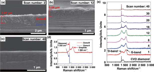
Figure 11. Cross-sectional SEM images and Raman spectra of the laser polished CVD diamond. (a)–(c) Cross-sectional SEM images of the sample at different laser scan numbers: (a) 2, (b) 12, and (c) 40; (d) Raman spectra at zones A and B of the cross-section, as shown in figure (a); (e) Raman spectra under different numbers of laser scans. [39] John Wiley & Sons. © 2021 Wiley-VCH GmbH.
Download figure:
Standard image High-resolution imageOkuchi et al [127] studied the ablation mechanism of nano-polycrystalline diamond (NPD) and SCD by nanosecond near-UV laser and femtosecond laser. Figures 12(a) and (b) show the TEM images of the ablation region profiles of NPD and SCD after nanosecond near-UV laser ablation, and figure 12(e) show the corresponding Raman spectra. It can be seen that there is an obvious graphitization layer on the surface of NPD and SCD after nanosecond laser ablation. According to figures 12(c) and (d), there is no obvious graphitization layer on the diamond surface after femtosecond laser ablation. There are only diamond peaks in the Raman spectrum of the diamond surface ablated by femtosecond laser, as shown in figure 12(e). Due to the low thermal impact depth and high efficiency of femtosecond laser ablation, the graphitization efficiency of the diamond surface during femtosecond laser ablation is lower than the ablation rate, so the graphitization layer is removed during the ablation process. These results indicate that the removal mechanism of PCD and SCD by laser ablation is basically the same, both of which are laser irradiation to graphitize their surfaces and then ablation to remove the graphite layer.

Figure 12. Cross-sectional TEM images of the ablation region by nanosecond near-infrared laser: (a) NPD and (b) SCD; cross-sectional TEM images of femtosecond laser ablation region: (c) NPD and (d) SCD, (e) Raman spectra of the ablated region of diamond [127]. Reproduced from [127], with permission from Springer Nature.
Download figure:
Standard image High-resolution image4.2. Material removal mechanism of IBP
IBP utilizes inert gas ion clusters or active plasma plume to impact material surfaces at high speed, eliminating differences in the surface curvature and redistributing surface quality [128]. This physical bombardment method is suitable for polishing various hard and brittle materials. During the process, ions penetrate the diamond surface, colliding with atoms inside the diamond, gradually softening the surface and heating and sublimating diamond lattice atoms due to the kinetic energy and ionization of the ions.
Zheng et al [50] treated CVD SCD with uniform underground cracking using hydrogen plasma. The chemical bond changes on the surface of SCD during the etching process were detected by x-ray photoelectron spectroscopy (XPS), and the etching mechanism of SCD was explored. It can be seen in figures 13(a) and (b) that the surface roughness of SCD significantly decreases as the etching time increases from 60 to 150 min. As shown in figure 13(c), there is an obvious sp3 peak at 284.9 eV in the C1s XPS spectrum before and after etching, which is mainly attributed to C–C/C–H bonds. There are also single oxidation CІ peaks (C–O–H, C–O–C, C–O–O–C) and double oxidation CⅡ peaks (C=O, O–C–O) in the XPS spectrum before etching. These two peaks are mainly caused by adventitious carbon or strong acid cleaning. Further, a sp2 hybrid peak appears in the XPS spectrum after 60 min of hydrogen plasma etching, which is mainly caused by α-C deposited on the surface of diamond. After 150 min of etching, the intensity of the sp2 hybrid peak decreases significantly. This indicates that the deposited α-C can be removed by hydrogen plasma etching to obtain high-quality SCD surfaces under sufficient etching time. According to figure 13(d), the two carbon-oxygen binding bonds before etching are also eliminated after etching. The strength of the sp3 (C–C/C–H) bond in figure 13(c) is enhanced after etching. This indicates that hydrogenation removal is likely to be the main mechanism for the removal of oxidized carbon and α-C on the diamond surface by hydrogen plasma etching.

Figure 13. Polishing quality and machining mechanism of IBP for diamond. AFM images of the SCD surface after etching for (a) 60 min and (b) 150 min; (c) C1s XPS spectra of the SCD before and after etching (for 60 min and 150 min, corresponding to figures (a) and (b)); (d) high-resolution O1s XPS spectra of the SCD before and after etching [50]. Reprinted from [50], Copyright (2022), with permission from Elsevier.
Download figure:
Standard image High-resolution imageMa et al [53] etched CVD diamond films with ECR plasma under an asymmetric magnetic mirror field to detect morphological changes on the film surface during etching and analyze the material removal mechanism during polishing. As shown in figure 14(a), the crystal shape and edges of the diamond film are clear before etching. However, as etching progresses, the original conical crystal gradually sinks and becomes blunt, leaving only small protruding fragments on the film surface after four hours of etching. The surface roughness Ra of diamond films decreases from 3.1 µm to 1.1 µm during the etching process. The Raman spectra of the CVD diamond films at different etching stages are shown in figure 14(e). The sp3-diamond bond peak is centered at 1332 cm−1, and a wide peak appears at 1430 cm−1 as etching proceeds. Weima et al [129] pointed out that this peak corresponds to sp2 hybrid amorphous carbon, indicating that high-energy ion bombardment gradually transforms the diamond phase into a graphite structure, resulting in smaller grain size on the film surface, sinking of the conical crystal, and lower roughness. However, it can be seen in figure 14(d) that graphite still exists on the surface of the etched diamond film. This is because the ablation rate of ECR plasma in this experiment is lower than the graphitization rate of diamond, so there is residual graphite on the surface after etching.

Figure 14. SEM images of diamond film at different etching stages: (a) before etching, (b) after 1 h etching, (c) after 2 h etching, and (d) after 4 h etching; (e) Raman spectra at different etching stages [53]. Reprinted from [53], Copyright (2014), with permission from Elsevier.
Download figure:
Standard image High-resolution image4.3. Material removal mechanism of PAP
Since the emergence of PAP technology, its material removal mechanism has received considerable research attention. Deng and Ji et al [130, 131] proposed the principle of PAP for SiC. As shown in figure 15, the SiC surface is first irradiated with atmospheric plasma. The free radicals in the plasma react with the surface atoms of SiC to form a modified layer with lower hardness. The modified layer is then removed by polishing with a soft abrasive plate. The chemical modification of the plasma and the friction removal of the polishing plate proceed synchronously, resulting in a smooth surface at the atomic level without damage. To explore the modification effect of plasma on SiC surface, Deng et al [132] obtained the cross-sectional TEM image of plasma-modified SiC surface using water vapor as the reaction gas. As shown in figure 15(b), a modified layer with a thickness of approximately 80 nm appears on the surface of SiC, and the main component of the modified layer has been transformed into SiO2 with lower hardness. According to the hardness test results in figure 15(c), the surface hardness of plasma-modified SiC is far lower than the original hardness [133]. This phenomenon confirms the speculated mechanism in figure 15(a).

Figure 15. Device and polishing effect of PAP on SiC. (a) Schematic of PAP for SiC [131]. Reproduced with permission from [131]. (b) Cross-sectional TEM image of SiC surface modified by plasma using water vapor as the reaction gas [132]. Reprinted from [132], with the permission of AIP Publishing. (c) Hardness of SiC before and after surface modification [133]. Reproduced from [133], with permission from Springer Nature.
Download figure:
Standard image High-resolution imageHowever, the material removal mechanism of PAP for diamond is inconsistent with that for SiC. Currently, researchers mainly believe that the material removal mechanism of PAP for diamond is plasma-induced oxidation of the polished plate surface, chemical reaction on the contact interface, and abrasion of the contact interface. Peguiron et al [134] proposed a SiO2 weakening model to explain the material removal mechanism of PAP for SCD with quartz glass as the polishing plate. The binding energy of the C–C bond can be weakened when silicon dioxide and diamond are ground together. Si–C and O–C bonds, with higher strength than the weakened C–C bond, can be generated at the diamond/silica interface. The adsorption between Si–C bonds and the relative motion between the polishing plate and diamond can remove the C atoms, thereby polishing diamond. The surface of the quartz glass plate of the polishing pad is illuminated by plasma during the PAP process. The O-removed silicon atoms on the quartz glass surface can be rapidly oxidized by the O atoms generated by Ar-based oxygen plasma, achieving a high MRR. Luo et al [51] fabricated a device for PAP of diamond and used atmospheric ICP to modify the silicon plates for efficient SCD polishing. Figure 16(a) shows a schematic of the polishing process. High-temperature ICP generates a large amount of OH radicals (–OH), which adhere to the surface of the silicon plate. The modified silicon plate transfers –OH to the diamond surface. High-temperature plasma rapidly increases the temperature of the contact interface between the silicon plate and diamond to several hundred degrees, providing sufficient activation energy for the repair of chemical bonds. –OH undergoes dehydration and condensation reactions at the polishing interface, forming chemical bonds such as C–C, C–O, Si–O, and C–O–Si. Luo et al [51] detected three main strong peaks of C1s, O1s, and Si2p on the polished diamond surface by XPS technology. As shown in figures 16(b)–(d), the chemical bonds corresponding to the three main strong peak areas are consistent with those described in the material removal mechanism diagram in figure 16(a). As Si is softer than diamond, the stripped Si fragments adhere to the diamond surface during grinding. Therefore, Si–Si and Si–O bonds are also detected on the polished diamond surface. Generally, the C1s region determines the change in the surface chemical properties during diamond polishing. According to figure 16(b), the binding energy of the C–C bond is relatively weak [135]. In addition, –OH is easily adsorbed on the protrusion of the diamond substrate, and the bonding energy at this position is relatively weak, so it can be easily removed by chemical mechanical action. Therefore, the C atoms on the diamond surface are removed under the shear friction effect of the two surfaces.

Figure 16. Material removal mechanism of ICP-enhanced PAP of diamonds. (a) Polishing process; (b)–(d) main photoelectron and Auger signals, and deconvoluted spectra of (b) C1s, (c) O1s, and (d) Si2p [51]. Reprinted from [51], Copyright (2021), with permission from Elsevier.
Download figure:
Standard image High-resolution imageMP can cause scratches or damage on the machined surface [30]. Although CMP offers low damage processing, its MRR is too low [33]. Additionally, the obvious anisotropy of the material removal process of CMP leads to weak flattening ability at the atomic scale [35]. By contrast, the plasma in PAP only modifies the polishing plate, and material removal primarily depends on the chemical reaction and abrasion at the contact interface between the polishing plate and the diamond. As a result, PAP combines the advantages of MP and CMP to achieve efficient and high-quality surface polishing.
4.4. Material removal mechanism of LAP
Watanabe et al [48] believed that UV LAP of SCD is a mechanochemical polishing method (MCP) combined with a UV light-induced photochemical reaction. Kubota and Takita [52] suggested that the interaction between the active substances and diamond substrate is the main reason for the high MRR of LAP. They explained the material removal mechanism of VUV-assisted polishing of diamond, as shown in figure 17(a). The polishing plate surface becomes super-hydrophilic after being irradiated by 172 nm VUV light and is covered by Al–OH bond groups. The modified polishing plate comes into contact with the diamond, and the active –OH covers the diamond surface. As shown in figure 17(b), –H and –OH combine to release a water molecule, resulting in a C–O–Al bond (see figure 17(c)). The binding energy of the C–O–Al bond is higher than that of the C–C bond. In the last step, as shown in figure 17(d), with the rotation of the polishing disc, the C–C bond is broken, and the C atom on the diamond surface is removed. To confirm that laser can induce oxidative removal on the diamond surface, Kubota and Takita [52] measured the XPS spectra of the C1s region of the diamond surface, and the results are shown in figures 17(e)–(g). A weak peak appears at 287.4 eV on the polished diamond surface after being irradiated by a VUV laser, which corresponds to the C=O bond. However, there are no such peaks on the polished diamond surface without VUV laser irradiation and the pre-polished diamond surface. This indicates that the VUV laser irradiation can induce oxidative removal on diamond surfaces.

Figure 17. Material removal mechanism of LAP for diamond. (a)–(d) Schematic of material removal mechanism in VUV-assisted polishing; (e)–(g) XPS C1s spectra of the diamond surfaces: (e) pre-polished diamond surface, (f) polished diamond surface without VUV irradiation, and (g) polished diamond surface with VUV irradiation [52]. Reprinted from [52], Copyright (2018), with permission from Elsevier.
Download figure:
Standard image High-resolution imageThe material removal mechanisms of PAP and LAP are similar as both methods utilize an energy beam to induce hydrophilicity on the surface of the polishing plate. Then, the diamond is ground through a modified polishing plate containing an active –OH group to remove the C atoms from the surface.
5. Influencing factors of energy beam-based direct and assisted polishing techniques for diamond
5.1. Influencing factors of LP
5.1.1. Laser type.
Over the recent years, numerous lasers have been used for diamond processing, including pulsed excimer [136], Nd-YAG [137], XeCl [138], and ArF [139] lasers. Short-pulse lasers are especially effective in achieving high-precision and sharp profiles while minimizing heat conduction into the bulk material [140]. Femtosecond pulses and an accelerating beam can be used to achieve curved profiles with micron-sized curvatures. However, nanosecond pulsed lasers can cause four types of damage: cracking, ripple formation, groove shape deformation, and debris deposition. These are caused by rapid temperature changes, laser reflection from groove walls, enhanced plasma absorption, and two different ablation regimes, respectively [141]. Ascarelli et al [126] compared the effects of nanosecond near-infrared, nanosecond near-UV, and femtosecond near-infrared pulsed laser processing on the surface of NPD. The findings revealed that infrared laser processing resulted in a rough surface, while UV and femtosecond laser processing produced satisfactory surface quality. Ogawa et al [97] compared the ablation quality of nanosecond and femtosecond lasers on PCD surfaces, and the corresponding results are shown in figure 18. It can be seen that the femtosecond laser is able to directly produce high-quality diamond surfaces with a roughness Ra of only 0.16 μm. However, there is significant residual graphite on the surface of diamond after nanosecond LP when the power difference is not significant. In addition, the MRR of femtosecond laser processing is better than that of nanosecond laser processing.
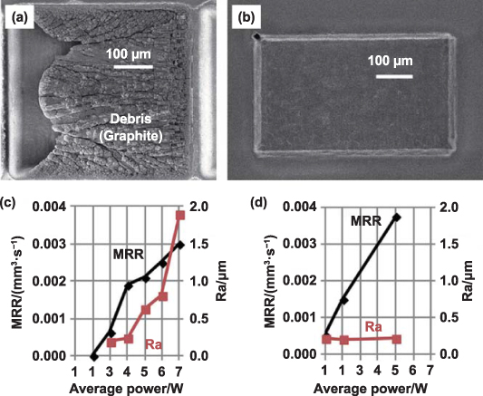
Figure 18. Machined surfaces obtained by normal irradiation of (a) nanosecond pulse laser (NSPL; average power: 6 W) and (b) femtosecond pulsed laser (FSPL; average power: 5 W); comparison of average surface roughness Ra and MRR by (c) NSPL and (d) FSPL (pulse pitch: 2 μm constant) [97]. Reprinted from [97], Copyright (2016), with permission from Elsevier.
Download figure:
Standard image High-resolution image5.1.2. Processing parameters of laser.
The intensity range of Nd-YAG lasers (106–107 W cm−2) is sufficient to vaporize diamonds and generate holes [142]. Beam parameters such as current, repetition frequency, feed velocity, spot diameter, and scanning speed affect the ablation quality and MRR [143]. The incident direction of the laser beam also affects this process significantly. When the beam is incident along the <100> crystal direction, laser-induced structural modifications prefer to propagate along the {111} planes when using visible and near-infrared ultra-short laser pulses [144–146]. Based on this property, a nanosecond-pulsed visible laser was used to obtain (111) planes of SCD by nucleating and propagating a mechanical cleave in the (111) plane. The obtained (111) planes showed atomically smooth surfaces and low kerf loss [147]. Additionally, the formation and morphology of bulk microstructures showed significant differences when the incident direction of the laser beam was changed from <100> to <110>, showing a higher breakdown threshold due to laser power depletion [148]. Komlenok et al [149] used femtosecond and nanosecond lasers to polish PCD plates with a roughness Ra of 5 µm and studied the effects of incidence angle, laser flux, scanning times, and scanning speed on the surface roughness. The experimental results showed that the surface roughness decreased with an increase in laser flux and scanning times when the incidence angle was constant, while the effect of scanning speed on the roughness was not significant. Prieske and Vollertsen [101] used a picosecond laser (wavelength: 515 nm, repetition rate: 200 kHz) to polish CVD diamond coating and studied the effect of laser flux and processing times on the polishing quality. As shown in figures 19(a)–(c), the sharp edges on the CVD diamond coating surface are removed by ablation when the laser flux increases from 0.31 to 0.52 J cm−2, and the surface quality is significantly improved. As shown in figures 19(d)–(f), the surface roughness Ra of CVD diamond decreases from 1.85 to 0.51 µm when the number of laser processing increases from 0 to 4. Wang et al [96] used a 248 nm pulsed excimer laser (wavelength: 248 nm, repetition rate: 20 Hz) to polish CVD diamond films and studied the effect of laser incidence angle on the polishing quality. As shown in figures 19(g)–(i), the RMS surface roughness of the diamond film reduces from 2.73 to 2.02 μm when the laser incidence angle increases from 60° to 80°. This indicates that within a certain range, the polishing quality of diamond improves with the increase in laser flux, scanning times, and incidence angle.
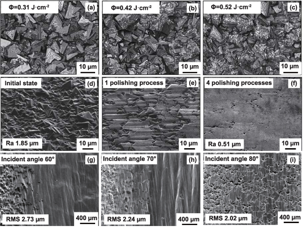
Figure 19. Influence of processing parameters on the polishing effect of LP for diamond. (a)–(c) Confocal laser images of CVD diamond surface ablated by different laser fluences (1 polishing process, incidence angle: 80°); (d)–(f) SEM images of CVD diamond surface under different scanning times (laser flux: 1.81 J·cm−2, incidence angle: 80°) [101]. Reprinted from [101], Copyright (2021), with permission from Elsevier. (g)–(i) SEM images of diamond film surface at different laser incidence angles (laser flux: 13.3 J·cm−2) [96]. Reproduced with permission from [96].
Download figure:
Standard image High-resolution image5.2. Influencing factors of IBP
5.2.1. Crystal orientation.
The anisotropy of SCD can significantly affect the etching quality of diamond surface using ion beam techniques. Naamoun et al [150] investigated the impact of crystal orientation on the shape of etch pits formed on the diamond surface using H2/O2 plasma. As shown in figures 20(a) and (b), etching along the <100> direction results in a rough surface with macro steps, and the minimum surface roughness Ra is 186 nm. Conversely, figures 20(c) and (d) demonstrate that etching along the <110> direction produces a smooth surface without pits, with a minimum surface roughness of Ra 15 nm.
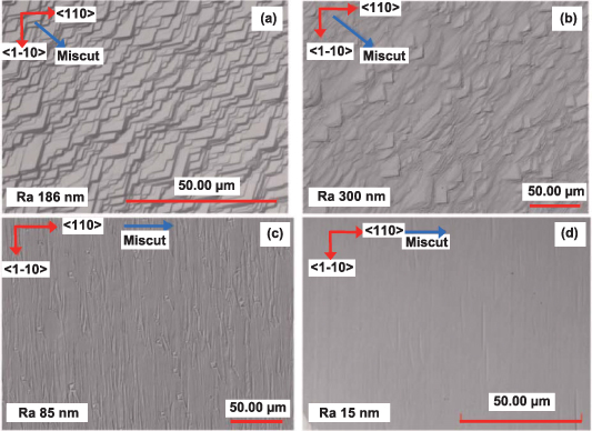
Figure 20. Optical microscopy images after H2/O2 plasma treatment. (a) Sample with 20° offset and (b) sample with 10° offset along the <100> direction; (c) sample with 10° offset and (d) sample with 20° offset along the <110> direction. [150] John Wiley & Sons. © 2012 WILEY-VCH Verlag GmbH & Co. KGaA, Weinheim.
Download figure:
Standard image High-resolution image5.2.2. Parameters of ion beams.
The incidence angle and ion dose are the main ion beam parameters that affect the polishing quality. Sato et al [116] used an Ar+-ion beam (1 keV) to grind the edges of PCD-coated tools and found that the surface roughness Ra decreased from 40 to 20 nm with an increase in the ion dose. Nagase et al [117] irradiated an SCD wafer with a 1 keV Ar ion beam at incidence angles of 0°, 30°, 45°, 60°, and 80° to study the effects of incidence angle and ion dose on the polishing quality. As shown in figures 21(a)–(f), the polishing quality is maximum when the incidence angle is less than 30°, and the RMS surface roughness can reach 0.10 nm. The polishing quality gradually decreases as the incidence angle increases from 45° to 80°. As shown in figures 21(g)–(i), the RMS surface roughness of diamond gradually decreases from 1.21 to 0.1 nm with the increase in ion dose from 3.6 × 10¹⁸ to 6.8 × 10¹⁸ ions cm−2, indicating that the polishing quality of diamond can be improved by appropriately increasing the ion dose.

Figure 21. Influence of processing parameters on the polishing effect of IBP. (a) AFM image of unprocessed diamond surface; (b)–(f) AFM images of the surface processed by ion beam with energy of 1 keV and ion dose of 6.8 × 10¹⁸ ions·cm−2 at incidence angles of 0°, 30°, 45°, 60°, and 80°; (g)–(j) AFM images under different ion doses at an incidence angle of 30° [117]. Reproduced with permission from [117].
Download figure:
Standard image High-resolution image5.3. Influencing factors of PAP and LAP
5.3.1. Crystal orientation.
The anisotropy of SCD usually affects the polishing quality of PAP and LAP. Luo et al [51] obtained the AFM images in different directions on the SCD (100) surface after PAP. As shown in figure 22, there is no obvious difference in the interface profile from 0° to 90°, which indicates that the anisotropy of SCD has no evident effect on the material removal process of PAP for diamond. This is because the material removal mechanism of PAP for diamond is mainly chemical reaction, thereby avoiding the anisotropic effects of mechanical removal. However, Watanabe et al [48] found that the anisotropy of SCD affects the polishing quality of UV LAP for diamond. It was observed that the surface roughness Ra of the (100) surface of SCD reached 0.21 nm after 60 min of polishing, while that of the (111) surface of SCD was only 0.34 nm after 270 min of polishing. These results confirm that the anisotropy of SCD influences the polishing quality of LAP. Overall, when using PAP or LAP to polish the SCD, there is no obvious quality difference in different crystal directions on the same crystal plane, but the roughness of different crystal planes can be different.

Figure 22. Surface quality and cross-sectional profile of SCD after PAP. (a) AFM image of SCD (100) surface after PAP, (b)–(e) sectional profile at different angles [51]. Reprinted from [51], Copyright (2021), with permission from Elsevier.
Download figure:
Standard image High-resolution image5.3.2. Type of reaction gas.
The type of reaction gas can also affect the MRR of PAP. Many types of gases can be used as the reaction gas for PAP, but the oxidizing strength of free radicals generated by the ionization of different gases varies. Deng et al [130, 131] used optical emission spectroscopy to compare the free radicals in two plasmas when the reaction gas was either water vapor or O2. As illustrated in figures 23(a) and (b), a strong signal of OH radicals (λ= 309 nm) is observed when water vapor is used as the reaction gas [151], and a strong signal of O free radicals (λ= 777 nm and λ= 845 nm) is observed when the reaction gas is O2 [152]. In addition, Deng [130] studied the effect of the oxidation of water vapor and O2 on the MRR through ball-disk friction experiments. As shown in figure 23(d), the MRR of SiC surface with water vapor as the reaction gas is significantly higher than that with O2 as the reaction gas. Since the oxidation potential of OH radicals (2.80 V) is greater than that of O radicals (2.42 V) [131], the MRR with water vapor as the reaction gas is higher than that with O2 as the reaction gas.
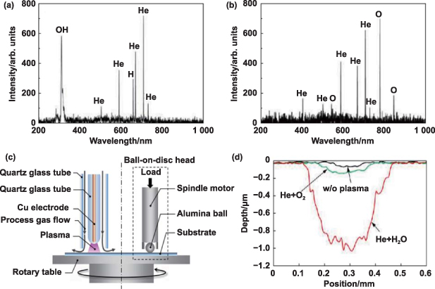
Figure 23. Optical emission spectra of plasma: (a) Water vapor-containing plasma, (b) oxygen- containing plasma. (c) Experimental device for ball-disk friction test, and (d) experimental results [131]. Reproduced with permission from [131].
Download figure:
Standard image High-resolution image5.3.3. Polishing plate.
It has been confirmed that the polishing quality of PAP is affected by the material of the polishing plate, rotation speed of the polishing plate, and contact pressure. Yamamura et al [123] investigated the impact of different types of polishing plate on the quality of PAP-processed SCD under argon plasma radiation with water vapor. Using a quartz glass polishing plate, the minimum surface roughness Sq was achieved to be 0.4 nm, while using sapphire polishing plate, it was 0.13 nm. Liu et al [119] examined the influence of polishing pressure and rotation speed of the polishing plate on the polishing quality. As illustrated in figures 24(a) and (b), the diamond surface after PAP exhibits grooves in the <100> direction with a change in sliding speed at a polishing pressure of 246.9 kPa, whereas no grooves are observed on the diamond surface at a polishing pressure of 62.5 kPa. In conjunction with figure 24(c), it can be inferred that the average roughness Sq of the diamond surface increases with an increase in the polishing pressure. The rotation speed of the polishing plate has no apparent effect on the surface quality of diamond processed by PAP. Figure 24(d) shows that the MRR of PAP increases with the rise in polishing pressure and plate rotation speed.
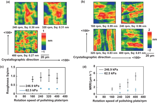
Figure 24. Effect of polishing pressure and rotation speed on the polishing quality of PAP. SWLI (84 μm2) images taken from SCD substrate after PAP with different rotation speeds of polishing plate at polishing pressures of (a) 62.5 kPa and (b) 246.9 kPa; influence of polishing pressure and rotation speed of polishing plate on the (c) surface roughness and (d) MRR of SCD substrate [119]. Reprinted from [119], Copyright (2022), with permission from Elsevier.
Download figure:
Standard image High-resolution imageDue to its high similarity to the equipment and material removal mechanism of PAP and LAP, the factors that affect PAP also have an impact on LAP. Therefore, the material and rotation speed of the polishing plate as well as the contact pressure affect the polishing quality of LAP.
5.3.4. Polishing time.
The irradiation of plasma and laser can introduce some small peaks and valleys, and the mechanical grinding effect of polishing plate also leaves scratches on the diamond surface. Therefore, during the early stage of the polishing process, the surface of diamond is rough. When the polishing time is sufficient, the polishing quality of PAP and LAP can meet the application requirements. Luo et al [51] studied the change in the surface roughness with polishing time during the PAP of SCD. As shown in figure 25(a), the surface roughness Sa of SCD is greater than 30 nm before 40 min. After polishing for 120 min, the surface roughness Sa of SCD reaches 0.86 nm. This shows that the polishing time has a significant impact on the polishing quality of PAP. Watanabe et al [48] studied the change in the surface roughness of PCD with polishing time during the UV LAP process of PCD. As shown in figure 25(b), the surface roughness of PCD substrates with different grains gradually decreases with the increase in the UV polishing time. This confirms that the polishing time has a significant influence on the polishing quality of LAP, and the surface accuracy of PCD substrate can meet the requirements only when the polishing time is sufficient.
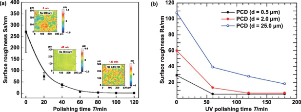
Figure 25. Effect of polishing time on the polishing quality of PAP and LAP. (a) Variation in the surface roughness with the polishing time during PAP [51]. Reprinted from [51], Copyright (2021), with permission from Elsevier. (b) Effect of UV polishing time on the surface roughness Ra of PCD substrates with different diamond grains [48]. Reprinted from [48], Copyright (2013), with permission from Elsevier.
Download figure:
Standard image High-resolution imageTable 8 summarizes the influencing factors of various energy beam-based direct and assisted polishing technologies. The main influencing factors of LP are laser type, laser parameters, and incidence angle. The influencing factors of IBP are crystal orientation, type of ion beams, ion dose, ion beam parameters, and incidence angle. The influencing factors of PAP and LAP are anisotropy of SCD, laser or plasma type, type of reaction gas, material of polishing plate, rotation speed of polishing plate, polishing time, and contact pressure.
Table 8. Influencing factors of various diamond polishing technologies.
| Technology | LP | IBP | PAP and LAP |
|---|---|---|---|
| Influencing factors | Laser type, laser parameters, incidence angle | Crystal orientation, type of ion beams, ion dose, parameters of ion beams, incidence angle | Anisotropy of SCD, laser or plasma type, type of reaction gas, material of polishing plate, rotation speed of polishing plate, polishing time, contact pressure |
6. Conclusions and outlooks
The unique physical and chemical properties of diamond make it a promising material in various fields, including semiconductor, optical, and precision machining. The surface polishing of SCD is particularly crucial for its practical applications, while the polishing of PCD tools and CVD diamond films is important for precision manufacturing. Energy beam polishing technology offers a promising solution, overcoming limitations of traditional polishing methods with enhanced efficiency and quality. Figure 26 summarizes the polishing effect, advantages, and disadvantages of energy beam polishing methods for diamond. Overall, this study provided a comprehensive review on the recent progress, material removal mechanisms, and influencing factors of various energy beam-based direct and assisted polishing technologies for SCD and PCD. The current key research focuses can be summarized as follows:
- (a)MRR. As the hardest material in the nature, machining diamond is extremely difficult and time-consuming. Increasing the MRR can effectively reduce the processing costs. LP has the highest MRR among the energy beam polishing technologies, typically ranging from tens to hundreds of microns per hour. PAP has the second highest MRR, typically up to 10 μm h−1. By contrast, IBP and LAP have the lowest MRR, usually less than 2 μm h−1.
- (b)Surface quality. For SCD, LP can cause thermal damage on the diamond surface and is only suitable for processing surfaces with a surface roughness of tens of nanometers. By contrast, IBP, PAP, and LAP can produce ultra-high precision surfaces with Ra below 0.5 nm. The CVD diamond films usually have an original roughness of several microns, much larger than that of SCD surfaces. Consequently, diamond films are typically polished using LP and IBP, and their surface roughness can reach tens to hundreds of nanometers.
- (c)Processing method. PAP and LAP are both contact and energy beam assisted polishing technologies. The corresponding polishing tools need to contact the sample surface and are usually only used for plane polishing. LP and IBP are non-contact and direct energy beam polishing technologies. The polishing tool does not need to contact the sample surface and can be used for planar and curved polishing of diamonds.
- (d)Cost assessment. LP has low costs due to simple equipment and low processing environment requirements. LP is usually used for efficient polishing of SCD substrates and CVD diamond films due to its excellent polishing efficiency. IBP, PAP, and LAP are typically only used for processing ultra-high precision diamond components due to their complex equipment and processing environment as well as high costs.
- (e)Influencing factors. The main influencing factors of LP and IBP are the type of energy beams, energy beam flux, incidence angle of the energy beam, and the anisotropy of SCD. The main influencing factors of PAP and LAP are the plasma or laser type, type of reaction gas, material of polishing plate, rotation speed of polishing plate, polishing time, contact pressure, and the anisotropy of SCD.
- (f)As a relatively new polishing technology, PAP causes less mechanical and chemical damages, and it can achieve high-efficiency and high-quality polishing of large-sized diamond substrates. However, the expensive equipment is the main reason that restricts the development of this technology.
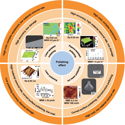
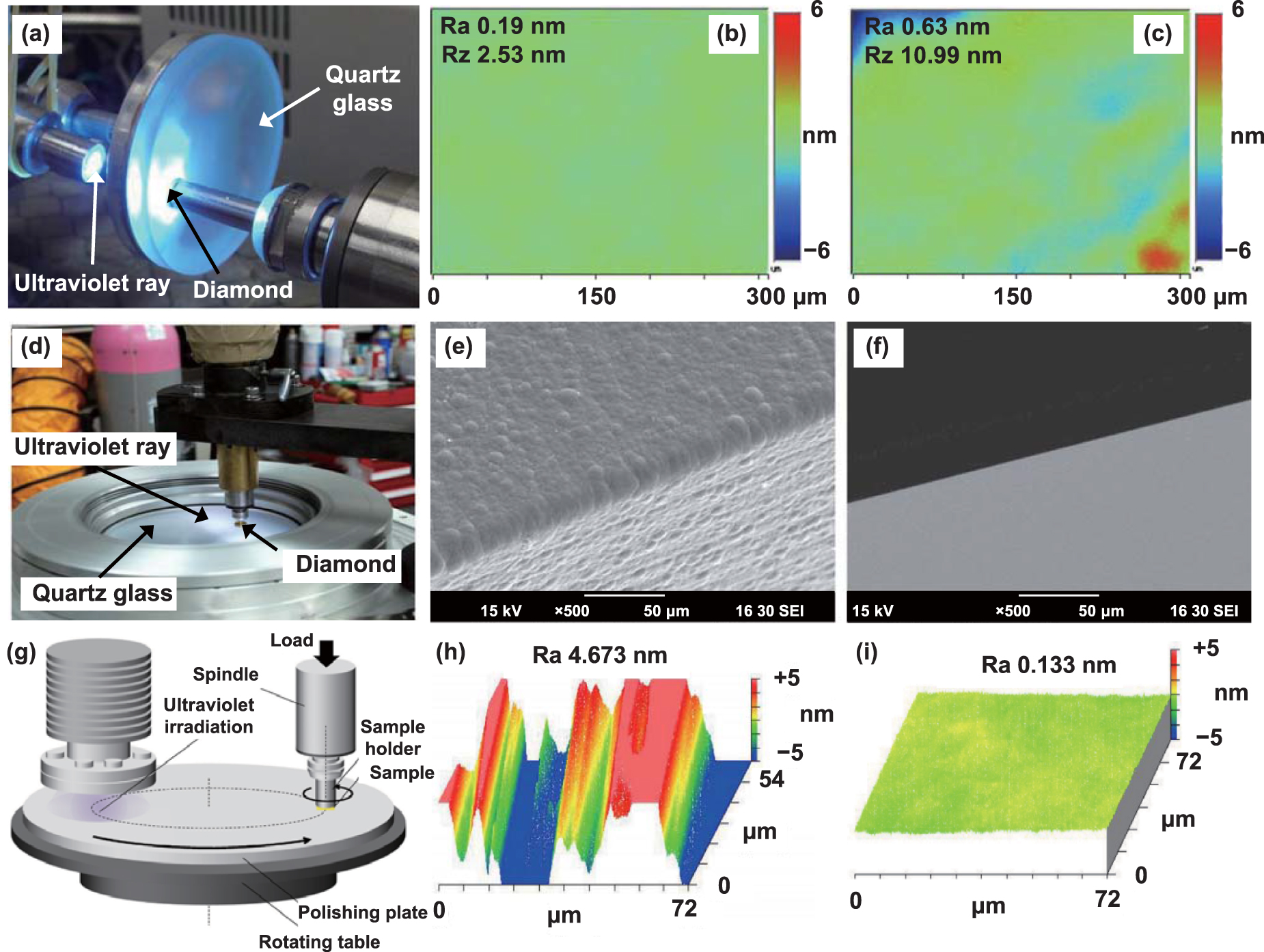
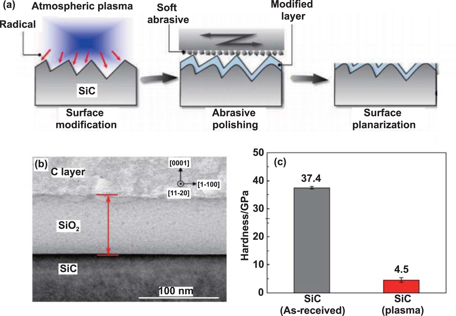
Figure 26. Polishing effect of various energy beam polishing technologies.
Download figure:
Standard image High-resolution image
The main limitations and future development directions of energy beam-based direct and assisted polishing diamond technologies are as follows:
- (a)Presently, the surface roughness obtained by LP is very limited. Therefore, it is crucial to improve the surface quality of LP-polished diamond by selecting a reasonable laser type or adjusting the laser and processing parameters.
- (b)The MRR of IBP is low, and the mechanical impact of the ion beam can easily damage the diamond surface. Therefore, improving the MRR and reducing the surface damage of IBP by optimizing the parameters and incidence angle of ion beams should be given considerable attention. In addition, obtaining high-quality diamond surface by using radioactive ion beam, FIB, ICP, or ECR plasma treatment is an important research direction in the field of IBP.
- (c)Although both PAP and LAP have extremely high polishing accuracy, their MRR is limited. The MRR of PAP and LAP can be effectively improved by changing the type of reaction gas and increasing the oxidation rate of the diamond surface. Additionally, the surface roughness and MRR can be improved by adjusting the rotation speed and contact pressure of the polishing disc. At present, the high equipment cost is still an important factor restricting the application of PAP and LAP in the diamond polishing field. Therefore, reducing the cost by improving the equipment structure can be of great practical significance.
- (d)LP has high MRR, while IBP, PAP, and LAP have high polishing accuracy. The combination of LP with IBP, PAP or LAP technology to develop more efficient and high-quality polishing techniques is of immense significance for the high-precision machining of diamonds.
Acknowledgments
This research is sponsored by the National Natural Science Foundation of China (Nos. 51835004, U22A20198), the Major Science and Technology Projects in Henan Province (221100230300) and the 111 Project (No. B23011)
Consent to participate
All authors agree to participate in this study.
Consent to publish
All authors agree to publish this paper.
Conflict of interest
The authors declare that they have no competing interests