
Abstract
The exceptional physical properties and unique layered structure of two-dimensional (2D) materials have made this class of materials great candidates for applications in electronics, energy conversion/storage devices, nanocomposites, and multifunctional coatings, among others. At the center of this application space, mechanical properties play a vital role in materials design, manufacturing, integration and performance. The emergence of 2D materials has also sparked broad scientific inquiry, with new understanding of mechanical interactions between 2D structures and interfaces being of great interest to the community. Building on the dramatic expansion of recent research activities, here we review significant advances in the understanding of the elastic properties, in-plane failures, fatigue performance, interfacial shear/friction, and adhesion behavior of 2D materials. In this article, special emphasis is placed on some new 2D materials, novel characterization techniques and computational methods, as well as insights into deformation and failure mechanisms. A deep understanding of the intrinsic and extrinsic factors that govern 2D material mechanics is further provided, in the hopes that the community may draw design strategies for structural and interfacial engineering of 2D material systems. We end this review article with a discussion of our perspective on the state of the field and outlook on areas for future research directions.
Highlights
The elastic properties, in-plane failures, fatigue performance, interfacial shear/friction, and adhesion behaviors of 2D materials are summarized.
Novel characterization techniques and computational methods are discussed.
Intrinsic and extrinsic factors that govern 2D material mechanics are further provided.
The challenges and perspectives in the field of 2D materials mechanics are outlined.
Export citation and abstract BibTeX RIS

Original content from this work may be used under the terms of the Creative Commons Attribution 4.0 license. Any further distribution of this work must maintain attribution to the author(s) and the title of the work, journal citation and DOI.
1. Introduction
The emergence of atomically thin 2D materials represents a theoretical limit of miniaturization. The monolayer format of 2D materials is particularly attractive, as it enables bottom-up synthesis schemes that facilitate spatial tailoring of physical properties. Through engineering of constituent interactions, the design flexibility provided by atomically thin materials presents an unprecedented opportunity for transformative breakthroughs in materials engineering. For example, field-effect transistors assembled from 2D materials such as graphene [1, 2] and MoS2 [3] possess high current ratios, presenting an opportunity for high-efficiency electronics. Additionally, 2D transition metal dichalcogenides (TMDs) such as MoS2 [4] have been demonstrated to have exceptional piezoelectric properties, which may be exploited for novel sensors, actuators, and energy harvesting applications.
In contrast to nanoscale electronic devices, however, advancements in the mechanics of 2D materials have been frustrated by the disconnect between the materials- and application-scales, although 2D materials exhibit unprecedented mechanical properties that offer an untapped potential for structural systems. For example, graphene oxide (GO) is reported (experimentally and computationally) to possess monolayer strengths in the range of 4–45 GPa [5–8], which are accessible through a directed failure of in-plane covalent bonds. Conversely, bulk GO papers have been reported to fail at tensile loads of ∼120 MPa [9], driven by interplanar shearing of monolayer stacks [10]. This disparity between in-plane and interplanar mechanical strengths is a general characteristic of 2D materials and represents a significant challenge toward the scalability of atomically-thin materials to structural dimensions. Within the context of materials design, tailoring and optimization of constituent interactions at the interfacial scale must be undertaken. The outcomes of this process should lead to an ideal transmission of in-plane and interplanar loads, which facilitates cohesive multiscale mechanical behavior while retaining high intrinsic strength. Recent efforts toward this design strategy have been undertaken in a variety of 2D material systems including graphene- [11–14], GO- [15, 16], and MXene-based [17, 18] composites.
The scaling of 2D materials into structural systems is an inherently multiscale challenge. The relations and properties required to bridge each length-scale are accessible using a combined experimental-computational approach, which leverages techniques that probe mechanical behaviors within regimes spanning the nano- to macro-scales. Indeed, experimental tools such as atomic force microscopy (AFM) testing are often paired with complementary computational simulations in order to measure the intrinsic properties of 2D materials [19, 20]. However, a systematic multiscale methodology, which can establish relationships that bridge length-scales and provide a predictive framework for hierarchical material properties, remains in progress. For example, the multiscale modeling of 2D-based structural materials requires a thorough characterization of constitutive behaviors, which can be unfeasible to measure using current experimental methodologies. Therefore, complementary computational studies based on density function theory (DFT) calculations or all-atom molecular dynamics (MD) simulations may be implemented in order to populate the material property space and to reveal the nanoscale deformation mechanisms of 2D materials. Products from these techniques may then be integrated into continuum-level approaches to provide multiscale predictions of mechanical properties. This workflow requires in-plane and out-of-plane property measurements to build constitutive laws for the mechanical behavior of 2D materials, which represents a focal point of this review.
The above-mentioned workflow has a series of challenges that need to be overcome. Beginning with the nanoscale, the difficulties with developing a multiscale model for 2D material hierarchies are reflected in the limitations of computing power, which restrict the complexity with which interatomic interactions may be described. In an effort to circumvent computational limitations, researchers are continuously developing new approaches and techniques, which provide efficient and high-accuracy descriptions of atomistic phenomena in 2D materials. For example, density functional theory-based tight binding (DFTB) calculations represent a computationally efficient method that provides accurate predictions of toughening mechanisms in epoxide-functionalized GO [5, 6].
Within the context of scalability, a long-standing limitation of atomistic modeling techniques such as DFT calculations and MD simulations remains the high computational cost inherent to these methodologies. In order to access larger length- and time-scales, researchers must employ reduced-order models such as coarse-grained (CG) MD. However, this homogenization process normally necessitates a concession of complexity, which ironically compromises the predictive nature of the simulation. Therefore, the scale-up of simulations to the mesoscale requires a trade-off between computational speed and accuracy. Despite these potential limitations, CG models have been developed for graphene [21] and GO [22], which accurately capture the experimental mechanical behavior. Another limitation in the scaling of computational efforts is the availability of interatomic potentials to accurately capture atomic interactions. Recent innovations in this space include the implementation of machine learning to provide accurate interatomic potentials for a wide range of material systems [23–26]. At the continuum level, the establishment of interfacial traction relationships between constituents is a challenging and critical step in the development of finite element method (FEM) simulations of 2D-based composite materials. To inform FEM simulations, a suite of experimental tools, such as AFM-based friction force microscopy (FFM) [27], may be leveraged to directly measure interfacial adhesion and cohesive behavior. Undoubtedly, the development of a multiscale predictive framework for 2D-based material systems requires an opportunistic utilization of complementary experimental and computational techniques, and continues to pose a significant challenge for the materials engineering community.
In this review, recent discoveries in the mechanics of 2D materials are discussed, including recently characterized mechanical properties, novel deformation mechanisms, characterization technologies, and computational advancements. The review is organized by mechanical properties: elastic properties, in-plane failure, fatigue, interfacial shear/friction, and adhesion, and concludes with the authors' outlook of the field. Under each section, an overview of recent experimental/computational technologies is introduced, followed by discussions of material-specific property measurements and deformation mechanisms. In sections where extensive studies were performed, a comparison or summary is also included. Section 2 focuses on elastic properties, particularly the in-plane and out-of-plane moduli. The array of corresponding experimental techniques, a review of the library of 2D materials that have been experimentally measured, as well as the applications of simulation-based approaches are also reviewed in this section. Section 3 introduces the measured in-plane failure properties of 2D materials along with the relevant developments in experimental techniques and atomistic simulation methods. Section 4 reviews fatigue behavior, with a focus on newly developed AFM- and cyclic tensile-based experimental methods and findings. Section 5 provides a review of the interfacial properties related to frictional and interfacial shear measurements between 2D material layers and substrates. Section 6 reviews the adhesive interactions between 2D materials and various mating surfaces. Lastly, section 7 discusses the authors' perspectives on future research directions in this field.
2. Elastic properties
Elastic properties, such as the in-plane and out-of-plane elastic moduli, define the recoverable deformation of 2D materials. This section introduces the array of experimental techniques, their limitations, and the current state-of-the-art. In addition, a review of the library of 2D materials for which the elastic properties have been experimentally measured is provided. While the focus of this section centers around the in-plane and out-of-plane moduli, the role of the bending stiffness in the elasticity of multilayer films, as well as the applications of simulation-based approaches to understanding the mechanics of 2D materials are also overviewed.
2.1. Methodology
2.1.1. AFM deflection testing.
AFM deflection testing is the most frequently adopted method for characterizing the mechanical properties of 2D materials, where a clamped, suspended membrane is loaded with an AFM tip positioned at the membrane center [28] (figure 1(a)). Typically, the deformation of 2D materials is stretching-dominated, resembling a membrane behavior, which can be described by:


Figure 1. Representative experimental setup and data analysis for characterization of the elastic properties of 2D materials. (a) Typical force-displacement curve and schematic of AFM deflection testing. [112] John Wiley & Sons. (b) In situ SEM tensile testing of a single crystalline suspended graphene sample based on a PTP micromechanical device actuated by an external instrumented indenter, giving rise to a uniaxial loading configuration. Reproduced from [113]. CC BY 4.0. (c) AFM linescans of the evolution of MoS2 bubbles with increasing pressure and the corresponding plots for CVD monolayer and bilayer devices with linear fits used to measure the modulus. Reprinted with permission from [42]. Copyright (2017) American Chemical Society. (d) Sketch of the process employed to fabricate the samples used in the surface wrinkling method and the obtained relationship between the wavelength of the wrinkles and the thickness of the MoS2 flakes. [49] John Wiley & Sons.
Download figure:
Standard image High-resolution imagewhere F is the applied force, σr is the pretension, δ is the deflection, E is the modulus, t is the thickness and a is the radius of the suspended membrane. As the force and deflection are recorded by AFM, the in-plane elastic modulus can be estimated by fitting the force-deflection curves, as depicted in figure 1(a). This approach has been widely used for in-plane stiffness measurement of many 2D materials, such as graphene and hexagonal boron nitride (hBN), which show an ultrahigh in-plane elastic modulus of up to 1 TPa [19, 20, 29, 30].
The study by Hone et al [19] also reported that graphene demonstrated nonlinear elasticity at high strains—a relatively uncommon behavior for a nominally brittle material. This unusual mechanical response emerges from graphene's large elastic limit when probed at the nanoscale (e.g. as by membrane deflection studies). However, the preservation of nonlinear elasticity over larger gauges is complicated by the presence of structural defects that cause failure below the intrinsic elastic limit of these systems [8]. In addition to nonlinear effects, the treatment of the elasticity of 2D materials and the associated workflows of mechanical testing have evolved significantly since the early studies. For instance, early works in graphene use isotropic elasticity to extract mechanical properties from the load-deflection curves of suspended membranes. However, as shown by Wei and Kysar [31], significant errors in the mechanical response arise at high deflections due to anisotropic effects, which can lead to a near ∼10% difference in measurements of uniaxial strength for pristine graphene (130 GPa [19] vs. 118 GPa [20]). Workflows pioneered by Wei et al [31, 32] combine first-principles calculations with continuum-level, finite element simulations. Using these tools, the nonlinear, anisotropic elastic relations for 2D materials can be determined, which serves as a cornerstone of the AFM deflection route for mechanical testing of 2D materials. More details regarding the AFM deflection technique that include the analytical models as well as the effect of prestress, boundary conditions, tip-sample interactions, and material nonlinearity can be found in a recent review by Cao and Gao [28].
2.1.2. Microelectromechanical systems (MEMS)-based tensile test.
While uniaxial tensile testing represents the most basic mechanical test of conventional materials, it is ironically difficult to perform in atomically thin films due to non-trivial challenges in handling and transfer. Yet, benefiting from advancements in electron microscopy and microfabrication technology, MEMS-based tensile devices have become powerful platforms for nanomechanical measurements of 2D materials. Typically, MEMS tensile devices consist of small actuators and diagnostic tools that enable the stretching of a sample under varying mechanical and electromechanical loading conditions. In contrast to AFM deflection tests, MEMS-based mechanical tests deliver uniform stresses along the in-plane direction of a 2D material, which is advantageous due to its simplicity of analysis. For instance, the measurement of elastic modulus at low strain is simply based on Hooke's law:

where σ is the uniaxial stress and  is the uniaxial strain, F is the applied load, Δl is the displacement, L, W and t are length, width and thickness of the 2D membrane respectively. Furthermore, the simplicity of the MEMS-based experimental setup facilitates the exploration of nonlinear elastic parameters of 2D materials. Under moderate to large deformations (e.g. > 5% for graphene [33]), the continuum thin shell theory gives the constitutive relationship
  , where the coefficient D is the third-order elastic modulus,
  and
and  . By fitting the F− Δl curve, both the second and third-order elastic constants E and D can be determined [34].
By using a novel push-to-pull (PTP) device, where loading and deformation measurement of specimens are performed with the aid of a nanoindenter. Lu's group [113] reported the measurement of the in-plane elastic modulus of chemical vapor deposition (CVD) synthesized single-crystal monolayer graphene (figure 1(b)). The obtained value was close to 1 TPa, approaching the ideal mechanical performance of graphene over a comparatively large area with edge defects. Such PTP-based tensile techniques have also been extended to hBN [35]. It was found that polycrystalline hBN monolayers displayed an in-plane stiffness of 200 N m−1, corresponding to an in-plane elastic modulus of ∼590 GPa. Based on a spring-like 'push-pull' mechanism, Lou's group [36] developed another type of in situ scanning electron microscopy (SEM) nanomechanical testing platform, consisting of three moveable shuttles attached to each other via inclined freestanding beams. It has been used to evaluate the in-plane elastic modulus of monolayer and bilayer MoSe2 as E = 177.2 ± 9.3 GPa.
In addition to the challenges in handling and transferring, several problems are left to be resolved. For example, focused ion beam (FIB) cutting is required to fabricate 2D material ribbons for MEMS-based tensile tests. It is technically difficult to control the irradiation dose to minimize the defects (e.g. edge defects), which degrade the mechanical properties of 2D materials. Furthermore, the effects of ribbon clamping usually act as stress concentrators which initiate cracking, which may lead to highly scattered results in mechanical measurements.
2.1.3. Bulging test.
Another approach to induce controllable and large biaxial strain fields is based on the bulging of a 2D membrane, which is obtained by establishing a pressure difference between the two sides of the membrane [37–39]. In contrast to the traditional bulging test that maintains a constant pressure, a micro-bubble device with constant molecule number was designed for 2D materials by Bunch's group [40, 41], leveraging the ultra-strong adhesion between 2D membranes and SiO2 substrates to prepare an impermeable seal for gas in the microcavity. Filling and emptying of the microcavity are accomplished by diffusion of gas through the interface, which is slow enough to allow reliable measurements of mechanical properties. According to the membrane analysis, the in-plane elastic modulus can be deduced from the measurement of bubble deflection (δ) and pressure difference (Δp) by:

where a is the hole radius, K(ν) is a non-dimensionless parameter, and t is the thickness. By measuring the bubble deflection at different pressures (figure 1(c)), Bunch and coworkers reported the in-plane stiffness of mechanically exfoliated and CVD-grown MoS2 to be 190 ± 35 N m−1 and 128 ± 20 N m−1, corresponding to an in-plane modulus of 283.6 ± 52.2 GPa and 191.0 ± 29.8 GPa, respectively [42]. The discrepancy in modulus between the exfoliated and CVD samples was attributed to the defects (e.g. grain boundary and vacancy) in CVD samples. Ultrathin aluminum oxide (Al2O3) films prepared by atomic layer deposition (ALD) were also mechanically characterized, showing an in-plane elastic modulus of 154 ± 13 GPa. This value is comparable to much thicker alumina ALD films, indicating high mechanical robustness with pinhole-free nanostructures [43].
It should be noted that the membrane analysis usually adopts clamped boundary conditions by assuming the thin films are perfectly adhered to the rigid substrates. However, the sliding of deflected membranes is commonplace at large deformations, which can result in different moduli depending on the interfacial interactions between 2D materials and substrates [44]. Wang et al [45] first experimentally revealed the interfacial shear deformation between monolayer graphene and a supporting SiO2 substrate through the pressurized bulging experiment, giving rise to an interfacial shear stress of 1.64 MPa. They found that the parameter K in equation (3) not only depends on Poisson's ratio but also the interfacial shear stress (τ), so that a more accurate in-plane elastic modulus can be obtained.
Recently, Wang et al [46] adopted the same approach to study the relationship between the in-plane elastic moduli and bending stiffness of three different 2D materials, including graphene, hBN and MoS2. The measured moduli coincide well with literature results, (Egraphene > EhBN > EMoS2), while the bending rigidity follows an opposite trend (Dgraphene < DhBN < DMoS2) for multilayers with comparable thickness, which is in opposition to the predictions within continuum mechanics frameworks. The abnormal bending behavior of multilayer 2D materials was demonstrated to result from the interlayer shear effect that is not captured by classical plate theory, which had been previously used to predict bending behaviors.
Compared to AFM deflection testing, the deformation of 2D materials in the bulging test is more uniform. Furthermore, an array of microbubbles can be simultaneously generated to allow high throughput experiments of 2D materials for statistical analysis of defects (grain boundary) or interfaces (stacking fault). However, the applied strain by bulging test is relatively low since the delamination of 2D materials tends to occur when the pressure approaches a critical value. Another limitation of the bulging test lies in its time-consuming process as the pressure is controlled by slow gas diffusion.
2.1.4. Surface wrinkling method.
Surface wrinkling has been widely exploited for the elastic measurement of thin films by studying the buckling instability, which arises when the film is deposited onto a compliant substrate loaded in uniaxial compression [47, 48]. The characteristic wavelength and amplitude of wrinkles only depend on the elastic properties of the film and the substrate, determined by:

where ν and νs are the Poisson's ratio for 2D materials and substrate, respectively, λ and h are the wavelength and amplitude of wrinkle, Es is the modulus of substrate (figure 1(d)). In such a way, Castellanos-Gomez's team [49] measured several 2D TMD materials with thicknesses ranging from 2 to 10 layers. The obtained moduli are consistent with those reported by AFM deflection tests.
The surface wrinkling method was also utilized for anisotropic 2D materials such as MoO3 and As2S3. For instance, the modulus of MoO3 along the a-axis (corner-sharing) and c-axis (edge-sharing) directions within an individual layer are 44 ± 8 GPa and 86 ± 15 GPa respectively, yielding an anisotropy ratio of ∼2 [50]. As2S3 was observed to display the largest in-plane mechanical anisotropy among reported 2D materials [51]. The moduli along zigzag and armchair directions are 51.5 ± 1.9 GPa and 16.7 ± 0.5 GPa respectively so the anisotropy ratio can be as high as ∼3.08.
In contrast to the abovementioned methods, the surface wrinkling method does not require freestanding samples so complex lithographic and transfer processes are avoided, which increases the measurement yield. Nevertheless, the stress in 2D materials on elastomer substrates relies on the interfacial load transfer which is usually considerably weak, thus lowering the strain level in samples. Additionally, the contact quality and adhesion between 2D materials and the substrate are highly non-uniform in the presence of wrinkles or contamination, which affects the strain distribution in 2D materials.
2.1.5. Micro-Brillouin light scattering (BLS).
BLS is a well-established non-destructive technique for mechanical testing of bulk condensed matter. It probes the light frequency shift resulting from inelastic light scattering on thermally populated acoustic waves [52, 53]. The mechanical properties of the material can be determined from phonon dispersion relations within the framework of classical elastodynamics. Graczykowski et al employed micro-BLS to determine the in-plane elastic modulus and residual stress of large-area MoS2 [54] membranes in a non-destructive manner. Assuming a Poisson ratio of 0.22, an in-plane elastic modulus of 22 GPa was estimated for a 5 nm thick membrane. This team further investigated the anisotropic elastic properties of few-nanometer-thick freestanding MoSe2 and observed that the moduli systematically decreased with a reducing number of layers. In particular, the measured moduli values for bilayers were 122 ± 3 GPa [55]. Note that, the most difficult aspect of the implementation of micro-BLS method is that it requires the use of specialized equipment for the mechanical measurement of 2D materials.
There are some less common but nonetheless valuable strategies to characterize the elasticity of a 2D material, such as indentation on microbubbles [56–59], bimodal AFM under amplitude/frequency modulation [60, 61], and dual-probe approach [62, 63] combining scanning probe microscopy with another characterization technique (e.g. scanning tunneling microscope, Raman spectroscopy, and SEM) to have full control of the local deformation and/or mechanical manipulation. We refer the reader to a recent review [64] focused on state-of-the-art local probe measurements of 2D materials for more details.
2.1.6. Computational methods.
Due to the early difficulties with the manipulation of 2D materials, first-principles atomistic simulations offer an accessible platform to probe the intrinsic mechanical properties of 2D materials. The advantage of these computationally led studies is that the mechanical properties can be directly probed by uniaxial tension, without the complex mechanics of AFM nanoindentation studies, which were the focus of contemporary experimental studies, as described above.
The earliest computational efforts naturally focused on monolayer graphene. Reports of the in-plane elastic properties from both DFT [65, 66] and MD [67–69] methods are well represented in the literature, with the latter relying primarily on reactive empirical bond order potentials to capture interatomic interactions [70, 71]. As the library of 2D materials has grown, so have analogous computational studies on the elasticity of these systems, with the uniaxial properties of GO [72, 73], graphene allotropes [74–77], hBN [78, 79], silicene [78, 80], phosphorene [81], several TMDs [82–84], and MXenes [85–87] reported in the literature. More recently, the community's emphasis on lateral and van der Waals (vdW) heterostructures has resulted in several computational studies of their fundamental mechanical properties [88–90]. Beyond uniaxial tension, computational studies offer the flexibility to investigate deformation modes that are difficult to probe directly by experiments. For instance, several studies report the bending [91–93] and in-plane shear [94, 95] responses of 2D materials. Furthermore, atomistic studies have also revealed exotic mechanical behaviors such as negative Poisson's ratios. Prominent examples of this behavior include a report from Jiang and Park [96] in phosphorene and a study from Jiang et al [97] in graphene stretched above 6% tensile strain.
In comparison to experiments, one advantage of computational studies is the rapid pace by which the mechanical properties of candidate 2D materials systems may be screened. For instance, Sun et al [74] report the elastic properties of 11 different graphene allotropes using DFT simulations. These allotropes are formed from monolayer tessellations of sp and sp2 hybridized bonds, which cover much of the parametric design space of carbon-based monolayer materials. From these studies, generalized equations have been proposed linking topological parameters such as the atom density [74] and bond orientation distribution [98] to the mechanical behavior, which serve as useful rules of thumb for judging the elastic properties of these systems. In addition to allotropes, computational methods also allow screening of the chemical design spaces in 2D systems, which can be vast for functionalized systems such as GO. Khoei and Khorrami [99] studied the mechanical properties of GOs using MD simulations. To provide a comprehensive examination of the GO property space, the authors varied the overall carbon-to-oxygen ratio and also the distribution of hydroxyl and epoxide functional groups.
Although computational workflows are attractive due to their accessibility, they suffer from some key limitations that merit discussion. Namely, while generally accurate, first-principles DFT methods are limited to extremely small simulation cells, which limits the measurement of complex systems with inherently large representative volumes. Furthermore, DFT simulations are relatively expensive, which limits their advantages in computational discovery. MD simulations are comparatively quick and offer a pathway to scale up or perform combinatorial atomistic simulations of 2D materials. Yet a disadvantage of this workflow is the limited interatomic potentials available to simulate the mechanics of 2D systems. Indeed, interatomic potentials are available for only a small handful of 2D systems (e.g. graphene [70, 100], GO [101, 102], TiC MXenes [103], MoS2 [104–108,114], MoSe2 [106], hBN [109], and phosphorene [105]). While reliable interatomic potential development is typically a time-consuming and delicate process, machine learning offers new opportunities to transform the traditional workflow by removing the requirement for domain expertise in the training of potentials. Chan et al [110] used a hierarchical objective genetic algorithm workflow to train a bond order potential for WSe2. New work from Zhang et al [111] uses a multi-objective genetic algorithm to parameterize interatomic potentials for large deformation in 2D materials. Studies leveraging machine learning in the mechanics of 2D materials are still emerging, but are anticipated to play a more significant role in research directions in the near future.
2.2. In-plane elastic modulus
The in-plane elastic modulus is one of the earliest mechanical properties of 2D materials to be experimentally measured. This parameter is often reported in standard units (e.g. GPa), but is fundamentally defined by a '2D modulus' or 'in-plane stiffness' (with units of N m−1), which is then transformed into the standard 3D in-plane elastic modulus value by normalization using an assumed monolayer thickness.
Beginning with graphene [19], much of the initial 'gold rush' has focused on the elastic modulus measurement of this 2D crystal, as the deformability is on one hand correlated with some potential applications such as stretchable electronics and nanoelectromechanical devices, and on the other hand, enables 2D materials to be modulated by elastic strain engineering [115, 116]. To date, the literature has been populated with an extensive catalog of measurements on a wide variety of 2D materials, such as TMDs, transition metal carbides and nitrides (TMCs and TMNs), covalent-organic frameworks (COFs), metal-organic frameworks (MOFs), perovskites, as well as the stacks of different 2D constituents, e.g. vdW heterostructures [117]. It has been demonstrated that the moduli of most 2D materials are thickness dependent, as shown in figure 2. The most recent data with further details are summarized in the sub-sections below.

Figure 2. Summary of the thickness-dependent in-plane elastic moduli for new 2D materials obtained by AFM deflection methods [112, 118–139].
Download figure:
Standard image High-resolution image2.2.1. TMDs.
TMDs are compounds composed of transition metal and chalcogen elements (sulfur, selenium, or tellurium [140]). In contrast to graphene and hBN, TMDs are typically semiconductive with tunable bandgaps in ranges appropriate for applications in next-generation opto-electronic devices. MoS2 is one of the most extensively studied TMDs, with triangularly packed layers of Mo atoms sandwiched between two layers of S atoms. Bertolazzi et al [118] first adopted the AFM deflection technique to characterize the elastic properties of MoS2 and obtained the in-plane elastic modulus of 270 ± 100 GPa and 200 ± 60 GPa for monolayers and bilayers, respectively. Castellanos-Gomez et al [119] later focused on multilayers (5–25 layers) and reported a higher value of 330 ± 70 GPa.
Across TMDs, transition metal (M) sulphides (MS2) usually have the highest elastic moduli, while tellurides (MTe2) are the softest. Sun et al [139] conducted temperature-variant AFM deflection tests on MoTe2, including the 2H, 1T', and Td phases. Due to similar atomic bonding, the three phases exhibited comparable in-plane elastic moduli of 110 ± 16 GPa for 2H-MoTe2, 99 ± 15 GPa for 1T'-MoTe2, and 102 ± 16 GPa for Td-MoTe2. The average value is only one-third of that for MoS2. Similar phenomena were also observed for other groups of TMDs. For example, the in-plane elastic modulus of monolayer WS2 is 279.8 ± 22.2 GPa, higher than that of WSe2 (250.7 ± 37.2 GPa), and almost double that for WTe2 (158.1 ± 9.8 GPa) [121]. The average in-plane elastic moduli of 12 nm-thick HfS2 nano-drumheads (45.3 ± 3.7 GPa) are slightly higher than those of HfSe2 with similar thickness (39.3 ± 8.9 GPa [124]). Differences in moduli between HfS2 and HfSe2 (∼6 GPa) tend to increase up to 60 GPa at higher thicknesses of around 30 nm because of the distinct interlayer bonding between adjacent layers in the two systems.
Within the family of TMDs, vanadium disulfide (VS2 [125]) is a special member in terms of its metallic nature, with a bandgap-free electronic structure. It was found that the in-plane elastic modulus is almost independent of the sample thickness, which slightly decreases from 49.6 ± 7.4 GPa to 40.3 ± 8.4 GPa as the thickness increases from 5.0 nm to 18.2 nm. This is in stark contrast with the obvious degradation tendency of in-plane elastic modulus for graphene due to the interlayer slippage during the indentation, suggesting relatively strong interlayer interactions for VS2 with the presence of interstitial V atoms within the vdW gap. It is also noted that VS2 appears to be the softest among TMDs, possibly due to relatively weaker atomic bonding compared to other systems.
2.2.2. TMCs and TMNs.
TMCs and TMNs, collectively referred to here as MXenes [141], are a relatively new member of the 2D materials family, having a general formula of Mn + 1Xn Tx , where M is a transition metal (Ti, Zr, Nb, etc), X is carbon or nitrogen, and Tx represents the surface bonded terminations, such as fluorine, oxygen, and hydroxyl groups. Since its discovery in 2011 by Yury Gogotsi et al, Ti3C2Tx has proven to be the most studied MXene material [142–144]. Lipatov et al [126] performed the first AFM deflection measurement of the in-plane elastic modulus for monolayer and bilayer Ti3C2Tx , which is reported to be 333 ± 30 GPa. The elastic properties of MXenes were also characterized on a PTP device by MEMS-based tensile testing [145], giving rise to in-plane elastic moduli of 217.8 GPa for Ti2CTx and 204.9 GPa for Ti3C2Tx , which demonstrates a much weaker thickness dependence than that previously observed in multilayer graphene and MoS2 stacks. This also suggests stronger interlayer strength between MXene layers due to an abundance of intercalated functional groups. In a quest for 2D MXenes with higher in-plane elastic moduli, Gogotsi's group [112] considered their bulk TMC counterparts, which are known for exceptional mechanical properties. It was reported that a cubic NbC crystal presented a higher modulus than that of cubic TiC, hence it is reasonable to speculate that Nb4C3Tx is stiffer than Ti3C2Tx . The AFM deflection experiments yield an in-plane elastic modulus of 386 ± 14 GPa, which is a new record for the elastic modulus of solution-processable 2D materials.
Beyond solution processing of TMCs/TMNs, Wang et al [127] synthesized atomically thin tungsten nitride (WN) crystals on SiO2/Si substrates by a salt-assisted CVD method. Interestingly, the modulus obtained from AFM deflection tests shows the lowest value of 230 GPa for the thinnest sample (3 nm thick), while thicker films (⩾4.5 nm) were found to have moduli no less than 370 GPa. The observed trend was ascribed to the oxidation of WN in air, resulting in the formation of surface defects that took a higher percentage of the volume for thinner layers.
2.2.3. COFs and MOFs.
COFs [146] have emerged as a new class of 2D crystalline nanoporous materials that consist of layers of 2D networks of organic monomers connected through covalent bonds. In contrast to the widely studied 2D materials (e.g. graphene and hBN) that offer few pathways for structural tailoring, COFs show a variety of architectures, pre-designed cavities, and chemical functionalities [147]. Through the synthesis at oil/water/hydrogel interfaces, Hao et al [136] successfully prepared a freestanding COF film, with thicknesses ranging from 4 to 150 nm. The mechanical measurements were performed by AFM deflection on a 4.7 nm-thick film, and the modulus is calculated to be 25.9 ± 0.6 GPa, which is higher than that of some common polymer materials like polymethylmethacrylate (PMMA) and polydimethylsiloxane (PDMS). Recently, Lou's group used a custom MEMS loading device to measure the tensile properties of 2D COFTAPB-DHTA films [148], where DHTA represents 2,5-dihydroxyterethaldehyde and TAPB denotes 1,3,5-tris (4-aminophenyl) benzene. As a result, the in-plane elastic modulus was measured to be 10.4 ± 3.4 GPa.
Similar to COFs, MOFs are a porous crystalline material constructed by the coordination bonding of metal ions or clusters with organic linkers [149, 150]. The variable chemical interactions ranging from strong coordination bonds to weaker dispersion forces and hydrogen bonding interactions, endow MOFs with significant structural flexibility in response to external stress [151]. The MOF topology and geometry can be further tailored to modify the mechanical performance [152]. An ultra-large laminar MOF of formula [Cu(μ-pym2S2)(μ-Cl)]n has been recently designed, whose thickness can be controlled down to 2 nm [153], allowing the preparation of suspended membranes for AFM deflection tests. The in-plane elastic modulus was estimated to be 5 GPa, approximately 200 times lower than that for monolayer graphene.
2.2.4. Perovskites.
2D hybrid halide organic-inorganic perovskites (HOIP) have caught intense attention as emerging semiconductor materials, showing huge potential in applications of high-performance photovoltaics [154, 155]. They can be conceptually derived from the 3D perovskites AMX3 (A = Cs+, CH3NH3 +, [HC(NH2)2]+; M = Pb2+, Ge2+, Sn2+; X = Cl−, Br−, I−), giving rise to the final formula (A')2(A)n − 1Pbn I3n + 1, where A' represents a large organic spacer and A denotes small organic cations [156]. Tu et al [129] have been dedicated to the mechanical studies of 2D HOIP based on AFM deflection methodology. They found that the in-plane elastic modulus of monolayer 2D Ruddlesden–Popper HOIP (C4H9-NH3)2(CH3-NH3)2Pb3I10 is only 11.2 ± 1.4 GPa due to the weak ionic bonding, much lower than other 2D materials that are covalently bonded in-plane. In addition, 2D HOIP tends to be softer with increasing thickness, with the modulus declining to 5.7 GPa for trilayers. The mechanism responsible for the drop in elastic properties is interlayer slippage at vdW interfaces during the deformation. Furthermore, the structure-property relationship was examined in detail by varying the halide ion and the length of the linear alkyl spacer molecules in the 2D HOIPs [157]. Generally, the stiffness of (C4H9-NH3)2PbX4 (abbreviated as C4PbX, where X = Cl, Br, or I) follows the trend of the Pb–X bond strength. As a result, C4PbBr and C4PbCl show a modulus of 8.1 ± 1.0 and 10.6 ± 0.6 GPa respectively, higher than that of C4PbI (5.7 ± 0.4 GPa). Increasing the length of the linear alkyl spacer molecules in (Cm H2m+ 1-NH3)2PbI4 from C4 to C6 can greatly lower the modulus to 0.7 ± 0.1 GPa, which is maintained when further elongating the chain length to C8 but slightly increases back to 1.3 ± 0.2 GPa in the case of C12. This can be attributed to the competition between the stiffness change of the inorganic layer due to the bond strength variation and octahedral distortion, the relative fraction of soft organic layers in the crystal, and the interface mechanical coupling arising from the interdigitation of the alkyl chains.
The in-plane elasticity of a series of phenethylammonium (PEA) methylammonium lead iodide crystals has been characterized by the surface wrinkling method [158]. The 2D HOIP presents with a general formula of (C6H5(CH2)2NH3)2(CH3NH3)n − 1[Pbn I3n + 1], abbreviated as (PEA)2PbI4(MAPbI3)n − 1, where n denotes the number of inorganic layers between the larger PEA cation layers in the unit cell. From wrinkling analysis, the in-plane elastic moduli are measured in the range of 2–4 GPa and exhibit isotropy. This lies in stark contrast to the DFT-derived values, which are five times higher than the experimental results and show a clear in-plane anisotropy. Here, the straining of 2D crystals is achieved through shear load transfer from a compliant substrate. Thus, it is the weak, isotropic interlayer interactions that dominate the elastic response under wrinkling deformation. In comparison, AFM deflection or MEMS-based tensile loading allows the stretching of strong chemical bonds within the inorganic 2D sheets, giving rise to higher measured values of in-plane elastic moduli.
In addition to the 2D materials mentioned above, notable efforts have been directed toward the mechanical characterization of other emerging 2D materials, including group-III chalcogenides (e.g. GaS/GaSe/GaTe [130] and InSe [134]), group-V chalcogenides (e.g. Bi2Se3 [132]), chromium trihalide (CrCl3 and CrI3 [131]), metal oxides (HfO2 [124] and SrTiO3 [128]), Bi2O2Se [138], and Cr2Ge2Te6 [135]. A summary of in-plane moduli of the 2D materials included in this review is provided in table 1 and figure 2.
Table 1. A summary of the in-plane moduli of the 2D materials included in this review.
| Material | Thickness (nm) | Modulus (GPa) | Measurement technique | References |
|---|---|---|---|---|
| Graphene | 0.34 | 1000 ± 100 | AFM deflection | [19] |
| Graphene | 0.34 | 1026 ± 22 | AFM deflection | [29] |
| Graphene | 0.68 | 962.7 ± 23.9 | AFM deflection | [29] |
| Graphene | 1.02 | 980.1 ± 9.9 | AFM deflection | [29] |
| Graphene | 2.72 | 942 ± 3 | AFM deflection | [29] |
| Graphene | 0.335 | 920 | MEMS tensile test | [113] |
| Graphene | 0.34 | 1147 | Bulging test | [45] |
| hBN | 0.35 | 865 ± 73 | AFM deflection | [29] |
| hBN | 0.7 | 881.4 ± 53 | AFM deflection | [29] |
| hBN | 1.05 | 805.9 ± 43.1 | AFM deflection | [29] |
| hBN | 1.4 | 872.2 ± 21.1 | AFM deflection | [29] |
| hBN | 1.75 | 824 ± 8.9 | AFM deflection | [29] |
| hBN | 2.1 | 846.7 ± 18.4 | AFM deflection | [29] |
| hBN | 3.15 | 856 ± 3 | AFM deflection | [29] |
| hBN | 0.35 | 590 | MEMS tensile test | [35] |
| hBN | 0.35 | 439.8 ± 77.3 | MEMS tensile test | [159] |
| hBN | Multilayer | 769.9 ± 12.9 | Bulging test | [46] |
| MoS2 | 0.615 | 270 ± 100 | AFM deflection | [118] |
| MoS2 | 1.33 | 200 ± 60 | AFM deflection | [118] |
| MoS2 | 9.225 | 330 ± 70 | AFM deflection | [119] |
| MoS2 | 0.65 | 264 ± 18 | AFM deflection | [122] |
| MoS2 | 0.65 | 283.6 ± 52.2 | Bulging test | [42] |
| MoS2 | Multilayer | 314.3 ± 8.4 | Bulging test | [46] |
| MoS2 | 3–11 layer | 246 ± 35 | Surface wrinkling | [49] |
| MoSe2 | 0.615 | 177.2 ± 9.3 | MEMS tensile test | [36] |
| MoSe2 | 1.29 | 122 ± 3 | Brillouin light scattering | [55] |
| MoSe2 | 0.7 | 238 ± 15 | AFM deflection | [36] |
| MoSe2 | 5–10 layer | 224 ± 41 | Surface wrinkling | [49] |
| WS2 | 0.62 | 302.4 ± 24.1 | AFM deflection | [121] |
| WS2 | 1.86 | 263.1 ± 33.7 | AFM deflection | [121] |
| WS2 | 0.65 | 272 ± 18 | AFM deflection | [122] |
| WS2 | 3–8 layer | 236 ± 65 | Surface wrinkling | [49] |
| WSe2 | 3.5 | 170.3 ± 6.7 | AFM deflection | [123] |
| WSe2 | 4.2 | 166.3 ± 6.1 | AFM deflection | [123] |
| WSe2 | 8.4 | 167.9 ± 7.2 | AFM deflection | [123] |
| WSe2 | 0.65 | 258.6 ± 38.3 | AFM deflection | [121] |
| WSe2 | 1.95 | 238.9 ± 29.4 | AFM deflection | [121] |
| WSe2 | 4–9 layer | 163 ± 39 | Surface wrinkling | [49] |
| WTe2 | 0.71 | 149.1 ± 9.4 | AFM deflection | [121] |
| WTe2 | 2.13 | 127.7 ± 18.1 | AFM deflection | [121] |
| MoTe2 | 3.6 | 87.8 | AFM deflection | [139] |
| MoTe2 | 6 | 99.7 | AFM deflection | [139] |
| MoTe2 | 6.7 | 112.5 | AFM deflection | [139] |
| MoTe2 | 9 | 104 | AFM deflection | [139] |
| HfS2 | 12.2 | 45.3 ± 3.7 | AFM deflection | [124] |
| HfSe2 | 13.4 | 39.3 ± 8.9 | AFM deflection | [124] |
| VS2 | 5.0–18.4 | 49.6–40.3 | AFM deflection | [125] |
| BP | 14.3 | 276 ± 32.4 | AFM deflection | [160] |
| BP | ⩾30 | 89.7 ± 26.4 | AFM deflection | [160] |
| InSe | 4.8 | 110.1 ± 13.4 | AFM deflection | [134] |
| InSe | 5.6 | 103.9 ± 22.3 | AFM deflection | [134] |
| InSe | 6.4 | 100.9 ± 20.1 | AFM deflection | [134] |
| InSe | 7.2 | 98.6 ± 16.4 | AFM deflection | [134] |
| GaS | 10 | 173 ± 15 | AFM deflection | [130] |
| GaSe | 10 | 81.9 ± 12.7 | AFM deflection | [130] |
| GaTe | 10 | 24.6 ± 16.0 | AFM deflection | [130] |
| Ti3C2Tx | 0.98 | 330 | AFM deflection | [126] |
| Nb4C3Tx | 1.26 | 390 | AFM deflection | [112] |
| WN | 3 | 260 | AFM deflection | [127] |
| WN | 4.5 | 400 | AFM deflection | [127] |
| WN | 12 | 370 | AFM deflection | [127] |
| COF | 4.7 | 26 ± 1 | AFM deflection | [136] |
| MOF | 10 | 23 | AFM deflection | [137] |
| Perovskite | 2.65 | 11.2 ± 1.4 | AFM deflection | [129] |
| Perovskite | 5.3 | 7.1 ± 0.9 | AFM deflection | [129] |
| Perovskite | 7.95 | 5.7 | AFM deflection | [129] |
| Cr2Ge2Te6 | 19.8 | 56.2 ± 8.2 | AFM deflection | [135] |
| Bi2Te3 | 9.5 | 18.7 ± 7 | AFM deflection | [132] |
| Bi2Se3 | 9.5 ± 2.5 | 20.7 ± 4.0 | AFM deflection | [132] |
| CrCl3 | 1.7 | 43.4 ± 4.4 | AFM deflection | [131] |
| CrCl3 | 8.5 | 2.2 ± 0.2 | AFM deflection | [131] |
| CrI3 | 1.4 | 3.6 ± 0.4 | AFM deflection | [131] |
| CrI3 | 6.3 | 1.6 ± 0.04 | AFM deflection | [131] |
| SrTiO3 | 14 | 250 | AFM deflection | [128] |
| HfO2 | 15 | 182.6 ± 54.3 | AFM deflection | [124] |
| Bi2O2Se | 8.64 ± 5.64 | 88.7 ± 14.4 | AFM deflection | [138] |
2.3. Factors influencing the elastic properties
As discussed above, the elastic moduli for a given 2D material from different studies exhibit significant scatter. The underlying mechanisms may rest on a variety of internal factors including structural defects, wrinkles/ripples, and interlayer shear, as well as external factors such as strain and temperature that modulate the structure-property relationship.
2.3.1. Structural defects.
The presence of defects is recognized to have a profound influence on the mechanical properties of 2D materials. Generally, structural defects include grain boundaries, vacancies, and dislocations [161]. In addition to the defect configuration, the density and distribution also play a critical role in the elastic deformation of 2D materials. In particular, grain boundaries are inevitable in the growth of large-area, polycrystalline CVD films, which are also known to lower the in-plane elastic modulus from the theoretical simulations [162]. Early experiments reported that CVD graphene exhibited a modulus of 161.8 GPa, which is around 1/6 of the values for exfoliated graphene [163]. Similarly, Suk et al [164] recently reported a reduction of modulus to an average value of 0.38 TPa for graphene membranes with small grains (1–2 μm) and a high density of grain boundaries, while larger grains (10–20 μm) give rise to greater values (figures 3(a) and (b)). In these comparisons, it should be noted that the suspended graphene samples were typically prepared by PMMA-assisted wet transfer, which may cause ripples or additional defects that account for mechanical softening [163]. In this respect, Lee et al [20] employed PDMS as transfer medium for dry transfer to avoid the adverse effect of contaminations and surface tension on suspended graphene membrane. With this effort, they demonstrated that the elastic modulus of CVD-grown graphene is identical to that of exfoliated pristine graphene, seemingly contradicting other reports.

Figure 3. Factors affecting the measurement of the elastic properties of 2D materials. (a) Pressure-displacement curves of graphene membranes composed of different grain sizes. The inset is a 3D image of a bulged graphene membrane with fringe patterns. (b) Distribution of the in-plane elastic modulus of graphene membranes as a function of the grain boundary density. The inset is the Raman map for G-band positions of polycrystalline graphene membranes. Reprinted with permission from [164]. Copyright (2020) American Chemical Society. (c) Schematic of an electrostatic actuation device to measure the elasticity of 2D materials. (d) The nonlinear stress-strain curve for graphene affected by thermal crumpling. (e) Temperature-dependent stiffness of graphene. The inset shows a cartoon illustrating the evolution of crumpling in a membrane under gradually increasing stress. Reproduced from [179]. CC BY 4.0. (f) In-plane elastic modulus of graphene and hBN nanosheets of different thicknesses. (g) Comparison between the shear strain energy in the sandwich beam structure and sliding energy in bilayer hBN. Reproduced from [29]. CC BY 4.0.
Download figure:
Standard image High-resolution imageFor graphene films with nanocrystalline grains, which exhibit an inherently large grain boundary density, the arrangement and configuration of defects are also known to affect mechanical performance. By inductively coupled plasma CVD and thermal CVD methods, Xu et al [165] devised an effective way to control grain sizes and grain boundary structures. Surprisingly, by engineering the grain boundary distribution in analogy to the 2D plum pudding structures, it was found that the graphene films with a high density of grain boundaries and without triple junctions possess an effective in-plane elastic modulus even higher than 1.3 TPa. One reasonable explanation for such discrepancy is that grain boundaries of CVD-grown graphene are microstructurally complex, presenting various types of pentagon-heptagon dislocation lines, and some of them are weakly connected or even disconnected, leading to distinct mechanical responses. While the triple junctions generate severe stress concentrations when closely connected, resulting in cracks during elastic deformation. The sparsely distributed and isolated grain boundaries resemble low-density point defects and account for the stiffening effect as discussed below. A larger number of sub-critical defects enables greater debonding energy to be dissipated between two grains during the fracture process.
The effects of point defects have been widely investigated through O2 plasma etching, He-ion bombardment, and Ar-ion irradiation. It was observed that the elastic modulus of graphene under O2 plasma exposure is maintained even at a high density of sp3-type defects. With increasing treatment time, the defect character was dominated by large-scale vacancy regions, which were demonstrated to significantly impair mechanical properties, leading to a halving of the modulus [166]. In contrast, the in-plane elastic modulus of monolayer graphene is reduced slightly but remains nearly constant (0.8 TPa) even under high-energy He-ion irradiation. Multilayer graphene displayed enhanced resistance to radiation damage, as sputtered carbon atoms can be trapped between layers and form interlayer crosslinking to partially restore the degraded modulus. Interestingly, by introducing a controlled density of point defects (vacancy content of ∼0.2%) via Ar-ion irradiation, a great improvement in the in-plane elastic modulus up to ∼1.6 TPa was realized for monolayer graphene [167]. This abnormal phenomenon was explained in terms of a dependence of the elastic coefficients on the momentum of flexural modes, whereby the enhanced thermal fluctuation suppressed the softening effect of vacancies [168]. While the in-plane elastic modulus of graphene could increase significantly due to the suppression of thermal rippling, the maximum value should not exceed the fundamental value (∼1 TPa) at the limit of a perfectly flat graphene membrane. Song and Xu [169] attributed the graphene stiffening to the areal expansion associated with geometrical distortion out of the plane. The thermal ripples may play a role in renormalizing the mechanical performance of graphene, increasing the bending rigidity while decreasing the in-plane elastic modulus. However, this effect is not necessary to explain the observed vacancy-induced stiffening effect under AFM deflection tests.
2.3.2. Thermal fluctuation.
Atomically thin crystalline membranes suffer from out-of-plane fluctuations at finite temperatures due to their ultralow bending stiffnesses [170, 171]. From theory, thermal fluctuations are claimed to renormalize the mechanical parameters of 2D materials [172, 173], for example, causing a dramatic reduction of the in-plane elastic modulus, an increase in the bending stiffness, and negative Poisson's ratio for micron-sized graphene samples, in comparison to their in-plane values. Some of the seminal work in this area is provided by Gao and Huang [174], who studied thermal fluctuations in graphene by MD and statistical mechanics methods. This effort provides several key findings that have guided the early work in the thermomechanics of 2D materials. For instance, the authors revealed the importance of anharmonic interactions between bending and stretching vibration modes in modulating the temperature dependency of in-plane thermal expansion and out-of-plane thermal contraction effects. Furthermore, this effort demonstrated the dependency of elastic properties on temperature and membrane size due to entropic contributions from thermal rippling. In a subsequent study [175], the authors further examined the entropic effects of thermal rippling on graphene-substrate interactions. An important outcome of this effort is the prediction of a rippling-to-buckling transition beyond a critical compressive strain, which may explain commonly observed morphological features (e.g. wrinkles) on supported 2D materials. In a theoretical development, Ahmadpoor et al [176, 177] used a variational perturbation method to expand the statistical mechanics treatment of the thermomechanics of 2D materials, which provides new analytical tools to examine anharmonic couplings. More recently, Chen et al [178] have introduced a multi-beam shear model to explore the finite temperature mechanics of multilayer 2D materials. In addition to the lateral size and thickness, the interlayer shear modulus was found to interplay with thermal fluctuations and hence the tangent biaxial in-plane elastic modulus. The role of thermal fluctuations in modulating mechanical behavior, although rigorously investigated in a number of theoretical studies, still requires validation from experimental data.
The effect of thermal fluctuations has been taken into account in the experiments probing the elasticity of freestanding graphene membranes by Bolotin's group [179]. A low-stress stretching was performed by electrostatic actuation in temperature ranges from cryogenic up to room values (figure 3(c)). In particular, when the device was cooled from 300 K down to 10 K, a stiffening of graphene from 58.8 GPa to 250 GPa was observed, since the amplitude of flexural phonons caused crumpling scales with temperature (figures 3(d) and (e)). Later, they conducted the pressurized bulging test to achieve a higher stress loading to uncrumple the graphene membrane [180]. The degree of crumpling was monitored by the measurements of strain via Raman spectroscopy and wide-field interferometric profilometry. As a result, a nonlinear Hooke's law in the stress–strain relationship was captured, where the first linear stage with modulus ∼1176.5 GPa, describes the stretching of C–C bonds, while the second stage corresponds to the uncrumpling of the graphene membrane.
These results imply that the mechanical properties of 2D materials can be engineered in a wide range by tailoring the amount of crumpling through strain engineering. In this case, Lopez-Polín et al [181, 182] reported an increased mechanical response of graphene when subjected to biaxial strains induced in pressurized membranes. The in-plane stiffness was found to have a two-fold enhancement at strains larger than 0.3%. The stiffening mechanism was ascribed to the suppression of thermal fluctuation by strain-induced flattening of graphene membranes.
Similar to [179], Storch et al employed laser interferometry to monitor the capacitively driven static displacement of graphene membranes in a cryostat and also observed a reduction of in-plane elastic moduli with increasing temperature [183]. In contrast with the thermally rippled membrane theory, the unusual observation was attributed to the effects of surface contaminants such as polymer residue. By studying the dynamic response of graphene across a wide temperature range (80–550 K), de Alba et al [184] demonstrated the same temperature dependence of in-plane elastic modulus based on the analysis of resonant frequency.
2.3.3. Interlayer slippage.
It has been well known that the interlayer shear resistance is low in most 2D materials, which is due to weak vdW interactions between atomically smooth crystal planes [185, 186]. For this reason, many of their bulk counterparts, such as graphite and MoS2, have been used in applications as solid/dry lubricants [186, 187]. This also leads to easy interlayer slip in 2D layered systems when subjected to stretching or bending, and in turn, the interlayer slip lowers the overall in-plane and bending stiffness.
Wei et al [188] reported a 'recoverable slippage' mechanism of multilayer graphene during cyclic AFM deflection tests. In view of the force-deflection curve, a kink can be identified as the onset of slippage, beyond which the deformation behavior deviates from the linear elastic model prediction. Upon unloading, a hysteresis is clearly present, which suggests energy dissipation through friction. Such interlayer slippage was found to reduce the modulus from 1.026 TPa for monolayer to 0.942 TPa for eight layers [29]. By comparison, hBN exhibited an almost constant modulus across varied thicknesses, as shown in figure 3(f). It was revealed that bilayer graphene energetically favors sliding under the large deflections close to the indentation center, while bilayer BN displays higher positive sliding energies under the same conditions, which resist relative movement between layers (figure 3(g)). Similarly, in the mechanical study of three different 2D TMDs [121], the in-plane stiffness of WS2 reduced most dramatically with increased thickness compared to WSe2 and WTe2, due to its minimal sliding energy, regardless of strain level. Interlayer sliding could be easily triggered and lead to stress concentrations on the bottom layers, resulting in reduced mechanical properties.
2.3.4. External factors.
As discussed above, increasing temperature or decreasing strain could intensify the thermal fluctuation of the 2D materials and reduce their in-plane elastic moduli. A similar uncrumpling mechanism was also demonstrated in AFM deflection experiments of graphene floating on water [189]. The large in-plane elasticity of graphene combined with its atomic thickness yields a crumple-prone topography, which results in wrinkles and creases upon manipulation on water [163]. Graphene membranes appear to be softer for small applied forces, since uncrumpling (instead of stretching) dominates the deformation of graphene. Beyond that, significant apparent softening of graphene was also observed under an electric field [190]. One study showed that the Raman spectra of graphene under a gate voltage exhibited a red shift with increasing voltage, indicating the elongation of C–C bonds. Accordingly, the binding energy of graphene decreased with the voltage. These observations present one mechanism for the field-induced softening effect observed in the mechanical properties of graphene.
2.4. Out-of-plane elastic modulus
Multilayer 2D materials feature significant mechanical anisotropy as they are strongly bonded in-plane via covalent bonds, whereas the interactions between layers are dominated by weak vdW forces. For example, although the in-plane elastic modulus can reach 1 TPa [19] in the case of monolayer graphene, the out-of-plane modulus of multilayer stacks is only ∼40 GPa [191]. While the in-plane elasticity of 2D materials has been extensively studied, the experimental quantification of out-of-plane elasticity in the 2D limit is still in a nascent stage. In contrast to the in-plane elastic modulus, which remains an intrinsic material property in the 2D limit, the out-of-plane elastic modulus exhibits a strong coupling to the supporting substrate. In this regard, this property transitions from an intrinsic property measurement in multilayers to a substrate-dependent value [192, 193]. This scaling effect must be taken into consideration when parsing the literature values of the out-of-plane modulus for few-layer 2D materials.
Using the AFM nanoindentation method combined with standard Oliver and Pharr analysis, Tu et al [194] investigated the out-of-plane moduli of perovskites, as presented in figure 4(a). A specific type of 2D HOIP, (C4H9-NH3)2PbI4, was studied, giving rise to a modulus of 3.3 ± 0.1 GPa. Clearly, increasing inorganic layers (composed of corner-shared PbI6 octahedra) leads to the enhancement of moduli up to almost 9 GPa for (C4H9-NH3)2(CH3-NH3)4Pb5I16. Besides, as the alkyl chain length increases, the fraction of the organic part increases so that a decrease in moduli is expected (figure 4(b)). It was concluded that HOIPs from the 3D metal–halide framework to 2D vdW bonded crystals significantly soften the materials.

Figure 4. Characterizations of the out-of-plane elastic moduli of 2D materials. (a) Typical load vs indentation curves of 2D layered HOIP. (b) The effect of alkyl chain length and layer number on the out-of-plane elastic modulus. Reprinted with permission from [194]. Copyright (2018) American Chemical Society. (c) In situ contact resonance AFM measurements during electrochemical cycling. [204] John Wiley & Sons. (d) Out-of-plane elastic modulus as a function of the indentation depth by the theoretical computation and experiment. Reprinted by permission from Springer Nature Customer Service Centre GmbH: Springer Nature, Front. of Phys. [60] (c) 2020. (e) Experimentally measured indentation curves for single-crystal SiC, ten-layer-thick epitaxial graphene, and ten-layer-thick epitaxial graphene oxide by sub angstrom-resolution indentation. (f) Experimental results of out-of-plane elastic modulus of GO as a function of relative humidity. The insets are schematics of the corresponding atomistic structures showing how water molecules fill the interlayer spacing. Reprinted by permission from Springer Nature Customer Service Centre GmbH: Springer Nature, Nat. Mater. [195] (c) 2015.
Download figure:
Standard image High-resolution imageTan's group [137] pioneered the out-of-plane mechanical studies of 2D MOFs by a substrate-supported AFM indentation method. In terms of the technical limitations of contact mechanics models, the analysis of the unloading strain rate was leveraged to precisely characterize the mechanical properties of Copper 1,4-benzenedicarboxylate (CuBDC) nanosheets. In order to satisfy the 10% indentation depth rule and minimize the substrate effect, the AFM nanoindentation experiments were performed on nanosheet stacks of sufficient thickness. It should be noted that the out-of-plane stiffness of the CuBDC nanosheets measured by a low unloading strain rate is highly scattered and overestimated, mainly due to the creep deformation that exaggerates the stiffness value. It was found that an augmented unloading strain rate surpassing ∼140 s−1 is necessary to circumvent the creep effect, yielding a modulus of 22.9 GPa in the through-thickness direction.
Gao et al [195] recently developed a sub-angstrom-resolution indentation method (figure 4(e)) and investigated the out-of-plane elasticity of few-layer graphene and GO films based on Hertzian contact mechanics as expressed by:
where Fz is the normal force, R is the tip radius, Z is the indentation depth,  with
with  and
and  being the Poisson's ratios and the in-plane elastic moduli of the sample and AFM tip respectively. It was noted that the out-of-plane modulus of ten-layer graphene is 36 ± 3 GPa, which is close to literature values for highly oriented pyrolytic graphite (HOPG). By comparison, ten-layer GO films were found to be softer (23 ± 4 GPa) due to the increased interlayer distance. Furthermore, the out-of-plane modulus of GO tends to increase with increasing intercalated water content, reaching a maximum when a full monolayer of water is produced (figure 4(f)). Yet, the formation of a second water layer leads to a modulus decrease.
More recently, the contact resonance (CR) AFM technique has been developed for the out-of-plane elasticity measurement. Compared to nanoindentation, CR AFM is based on a comparative method that is conducted on a test sample, and a reference sample with a known modulus, thus avoiding the complicated calibration of tip parameters. When the tip makes contact with samples, a slight vertical modulation is introduced to either the cantilever base or the sample, and the values of the cantilever CR frequency and quality factor change in response to the elastic coupling (figure 4(c)). By using the CR AFM technique, Cheng's group [60] reported the out-of-plane moduli of SnSe to be in the range of 55–61 GPa, as shown in figure 4(d). Note that, in the theoretical model the interactions between non-adjacent layers were neglected since their strengths were claimed to be considerably weaker than those of the adjacent-layer interactions (<0.1). However, extensive works have demonstrated that monolayer 2D materials can only partially screen out mechanical interactions with supporting or neighboring materials [196], likely invalidating such assumptions.
A similar problem also exists for the low-frequency Raman technique, which offers another route to estimate the interlayer coupling for multilayer 2D materials [197, 198]. Typically, a linear chain model is adopted, where each atomic layer is simplified as a bead and interlayer interactions are modeled as springs. Assuming that interlayer interactions are dominated by interactions between nearest neighbor layers, and the force constants that describe the interlayer coupling strength do not change significantly with increasing layer number, a simple model links the interlayer force constant (α) with Raman peak positions (ω) and layer number (N):
where c is the speed of light, μ is the mass per unit area of a monolayer 2D material [199–201]. Raman breathing modes of various 2D materials have been examined using this method, yielding the out-of-plane moduli of 52.0 GPa for MoS2 and 52.1 GPa for WSe2 [202]. However, as mentioned above, although the frequencies of low energy Raman modes in multilayer 2D materials can be perfectly fitted by the linear chain model with only the nearest neighbor interactions, the assumption of constant interlayer interactions independent of layer number may not be valid. Wang et al [203] pointed out that, if the second nearest neighbor interaction is taken into account, the Raman frequencies of multilayer 2D materials (except bilayer) would increase or decrease depending on the second nearest neighbor force constant, leading to an underestimation or overestimation of out-of-plane elasticity.
3. In-plane failure
In-plane failure refers to the processes by which 2D materials break and it is quantified by a variety of parameters in the literature. In the ideal limit, in-plane failure is bounded by the intrinsic strength of 2D materials, which may be viewed as the stress required to break bonds between atoms in a monolayer. Beyond this ideal consideration, fracture toughness provides a more practical measure of in-plane failure as it specifies the loading conditions for the growth of a crack from a pre-existing flaw. Within the context of 2D materials, the most relevant predictor of fracture toughness is given by Griffith's criterion, which is a normalized measure of energy required to separate cleaving surfaces. Plasticity mechanisms, such as crack-tip blunting, provide additional toughening pathways beyond Griffith's basic definition, which can contribute to the fracture toughness of 2D materials. This section provides a review of the measured in-plane failure properties of 2D materials. This discussion begins with an overview of experimental techniques and their limitations. Following this, pathways to engineer the fracture properties of 2D materials are overviewed. In addition to these topics, atomistic simulations of in-plane failure are also reviewed, with a focus on atomic-scale analysis of defect mechanics and fracture toughening mechanisms.
3.1. Methodology
3.1.1. AFM deflection testing.
Beyond the elastic limit, pristine 2D materials generally experience brittle failure in response to further straining. The maximum stress at which a 2D flake fails characterizes the fracture strength. In 2D materials, fracture strengths are among the highest measured, which presents another extraordinary property of these systems. The most widely used experimental technique to measure fracture strength is AFM deflection testing, whose analysis builds from the workflows described in the elasticity sections.
The fracture strengths for different 2D materials are summarized in table 2 and figure 5(a). According to Griffith theory [209], the upper theoretical limit of fracture strength for defect-free brittle materials is around 1/9 of the elastic modulus. As shown in the figure 5(a), the fracture strengths of pristine monolayer 2D materials, such as graphene, hBN and MoS2 [19, 29, 118], are in excellent agreement with this theoretical prediction (1/9 of elastic modulus), highlighting the ideal behavior of these systems in small-scale testing. In contrast, the strength values for multilayer or defective/functionalized 2D materials (e.g. MXene [126, 210] and GO [7]) are lower than the theoretical prediction, due to the interlayer shear or defect-induced weakening, which will be discussed in detail below. One weakness of AFM membrane deflection experiments is the assumption of linear elasticity and isotropy in the measurement of in-plane strength ( ), where σ is the fracture strength, F is the breaking force, E is modulus, R is tip radius, and t is thickness, which often leads to overestimation of fracture strength in systems that exhibit non-linear and anisotropic responses. For example, taking the in-plane non-linearity into account in the constitutive stress–strain relation, a biaxial fracture strength of ∼100 GPa [20, 32] was predicted for graphene, which is lower than the value (130 GPa [19]) obtained using the linear elastic and isotropic workflow. Another issue worthy of scrutiny is the anisotropic fracture strength in terms of the preferred crack extension along zigzag edges [211, 212], which has been largely neglected in the mechanical analysis.
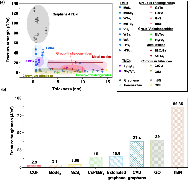
Figure 5. Overview of failure properties of typical 2D materials. (a) Summary of the thickness-dependent fracture strength for 2D materials obtained by AFM deflection methods [19, 29, 30, 112, 118–126, 128–134, 136–139]. (b) Comparison of fracture toughness among several 2D materials [36, 148, 159, 205–208].
Download figure:
Standard image High-resolution imageTable 2. The in-plane strength of the 2D materials included in this review.
| Material | Thickness (nm) | Strength (GPa) | Measurement technique | Reference |
|---|---|---|---|---|
| Graphene | 0.34 | 130 | AFM deflection | [19] |
| Graphene | 0.34 | 125 | AFM deflection | [29] |
| Graphene | 0.68 | 107.7 ± 4.3 | AFM deflection | [29] |
| Graphene | 1.02 | 105.6 ± 6 | AFM deflection | [29] |
| Graphene | 2.72 | 85.3 ± 5.4 | AFM deflection | [29] |
| hBN | 0.335 | 70.5 ± 5.5 | AFM deflection | [29] |
| hBN | 0.67 | 68 ± 6.8 | AFM deflection | [29] |
| hBN | 1.05 | 76.9 ± 2.3 | AFM deflection | [29] |
| hBN | 0.35 | 7.9 ± 2.5 | MEMS tensile test | [159] |
| MoS2 | 0.65 | 22 ± 4 | AFM deflection | [118] |
| MoS2 | 1.3 | 21 ± 6 | AFM deflection | [118] |
| WTe2 | 0.7 | 6.4 ± 3.3 | AFM deflection | [121] |
| WTe2 | 2.1 | 40.9 ± 6 | AFM deflection | [121] |
| MoSe2 | 0.7 | 3 ± 1 | AFM deflection | [36] |
| MoSe2 | 1.4 | 6 ± 3 | AFM deflection | [36] |
| WS2 | 0.62 | 47 ± 8.6 | AFM deflection | [121] |
| WSe2 | 0.65 | 38 ± 6 | AFM deflection | [121] |
| WSe2 | 1.95 | 35.5 ± 5.4 | AFM deflection | [121] |
| MoTe2 | 9.5 | 18.7 | AFM deflection | [139] |
| MoTe2 | 3.6 | 7.3 | AFM deflection | [139] |
| MoTe2 | 6 | 4.6 | AFM deflection | [139] |
| MoTe2 | 6.7 | 7 | AFM deflection | [139] |
| MoTe2 | 9 | 2.8 | AFM deflection | [139] |
| VS2 | 9.2 | 4.6 ± 0.2 | AFM deflection | [125] |
| HfS2 | 12.2 | 5.7 ± 0.4 | AFM deflection | [124] |
| HfSe2 | 4.5 | 4.5 ± 1.4 | AFM deflection | [124] |
| COF | 50 ± 5 | 0.75 ± 0.34 | MEMS tensile test | [148] |
| Perovskite | 2.7 | 0.7 ± 0.08 | AFM deflection | [129] |
| Perovskite | 5.3 | 0.44 ± 0.03 | AFM deflection | [129] |
| Perovskite | 7.7 | 0.36 ± 0.04 | AFM deflection | [129] |
| Perovskite | 10.6 | 0.35 ± 0.05 | AFM deflection | [129] |
| Ti3C2Tx | 0.98 | 17.3 ± 1.6 | AFM deflection | [126] |
| Ti3C2Tx | 6.86 | 9.98 | MEMS tensile test | [145] |
| Ti2CTx | 12.24 | 9.61 | MEMS tensile test | [145] |
| Ti2CTx | 35.36 | 7.59 | MEMS tensile test | [145] |
| Nb4C3Tx | 1.26 | 26 ± 1.6 | AFM deflection | [112] |
| SrTiO3 | 4 | 7.53 | AFM deflection | [128] |
| SrTiO3 | 8 | 6.9 | AFM deflection | [128] |
| SrTiO3 | 14 | 6.39 | AFM deflection | [128] |
| Bi2O2Se | 8.64 ± 5.64 | 20.5 ± 2.5 | AFM deflection | [138] |
| Bi2Te3 | 5 | 0.4 ± 0.08 | AFM deflection | [132] |
| Bi2Se3 | 9.5 ± 2.5 | 1.278 ± 0.29 | AFM deflection | [132] |
| CrCl3 | 1.7 | 2.2 ± 0.5 | AFM deflection | [131] |
| CrCl3 | 8.5 | 2.2 ± 0.2 | AFM deflection | [131] |
| CrI3 | 1.4 | 3.6 ± 0.4 | AFM deflection | [131] |
| CrI3 | 6.3 | 1.6 ± 0.04 | AFM deflection | [131] |
| GaS | 10 | 7.87 | AFM deflection | [130] |
| GaSe | 10 | 4.07 | AFM deflection | [130] |
| GaTe | 10 | 1.78 | AFM deflection | [130] |
| InSe | 6.4 | 8.68 | AFM deflection | [134] |
3.1.2. In situ transmission electron microscopy (TEM) tensile testing.
Though the intrinsic strength of 2D materials is critical in determining the service life and performance of nanodevices, it is their fracture toughness that is perhaps the most significant practical parameter. In contrast to the in-plane strength, which is considered the maximum stress that the defect-free material can sustain, fracture toughness is a property that describes the ability of a material containing a crack to resist fracture by propagation of the flaw. Since AFM deflection testing is unable to capture the crack initiation and propagation of 2D materials, MEMS-based in situ tensile testing under electron microscopy is frequently adopted to measure the fracture toughness (figure 6(a)). Typically, a central pre-crack with an initial length (2a0) <10% of sample width is created by FIB milling. Upon the fast fracture under uniaxial tension, the critical stress of the onset of fracture (σc) is captured to allow the estimation of the fracture toughness using Griffith analysis:


Figure 6. Representative experimental techniques for the characterizations of in-plain failure of 2D materials. (a) In situ TEM setup for tensile test of pre-cracked GO nanosheet. From [205]. Reprinted with permission from AAAS. (b) Fracture testing TEM image of the nanosheet with a V-shaped notch. Reprinted with permission from [213]. Copyright (2015) American Chemical Society. (c) Schematic of Raman spectroscopy and optical microscopy image of a crack tip zone for Raman mapping (boxed by red dashed lines), and stress distribution for the region boxed. Reprinted with permission from [207]. Copyright (2019) American Chemical Society. (d) Direction of crack propagation for different crystallographic orientations of the graphene flake. [214] John Wiley & Sons. (e) Schematic and SEM images demonstrating wrinkles and cracks on the surfaces of the graphene film during the tension test, and the evaluation of the fracture response of graphene based on the measurement of crack spacing. Reprinted with permission from [215]. Copyright (2016) American Chemical Society.
Download figure:
Standard image High-resolution imageUsing this technique, the fracture toughness of monolayer polycrystalline graphene was first measured to be 15.9 J m−2 [206], corresponding to the critical stress intensity factor of 4.0 ± 0.6 MPa . Later studies of other 2D systems revealed similar brittle behaviors. For instance, brittle failure was observed for MoSe2 [36], where a fracture toughness of 3.1 J m−2 was measured by DFT calculations. By contrast, GO nanosheets exhibit a comparatively high fracture toughness of ∼39 J m−2 [205], due to the interactions among functional groups in constituent layers and distinct fracture pathways in individual monolayers (figure 6(b)).
In addition to the MEMS-based tensile test, Wei et al [213] developed a novel in situ fracture toughness testing method for 2D materials with a special notch tip. The 2D nanosheet was clamped and loaded between the AFM and tungsten tips at its upper edge in high-resolution TEM, as shown in figure 6(b). Based on the finite element analysis of the stresses at the notch tip, the critical stress intensity factor of graphene and boronitrene are estimated to be 12.0 ± 3.9 and 5.5 ± 0.7 MPa , corresponding to the fracture toughness of around 144 and 36.2 J m−2 by using in-plane elastic moduli of 1.006 TPa and 0.836 TPa, respectively. The higher values of toughness for graphene in this study might be attributed to layer stacking which offers additional energy dissipation during crack propagation.
3.1.3. Raman-tensile testing.
Recently, Raman spectroscopy has also been employed as a technique to monitor the evolution and propagation of cracks in graphene deposited on a flexible substrate under uniaxial tension. In contrast to the brittle fracture of freestanding samples, the propagation of cracks in supported graphene can be clearly captured with the assistance of mild stress transfer from the substrate. Since the Raman 2D band is commonly regarded as the strain indicator due to its high sensitivity, it can be used to visualize the development of strain fields around the crack tip of the graphene, as depicted in figure 6(c) [207]. The corresponding contour of the stress under the load can also be obtained by multiplying the in-plane elastic modulus of graphene with the strains derived from the frequency shifts. Combined with the measurement of half the initial length of the crack (a0), an average fracture toughness of 37.4 ± 6.7 J m−2 was predicted for graphene according to the Griffith criterion (equation (7)). The relatively large fracture toughness was explained by the polycrystalline microstructure and blunt crack tip. A similar phenomenon was also observed by Zhao et al [214], where a sharp crack was found to occur at a critical stress intensity factor of 4.0 MPa , while a blunt crack showed a less localized stress field at the crack tip and propagated at a value of >9 MPa
 . The crack growth direction was further investigated. It was noted that cracks were prone to align approximately perpendicular to the tensile direction, regardless of the crystallographic orientation of the graphene (figure 6(d)). This Raman-based method enables the fracture behavior of cracks to be analyzed without the need to accurately measure the crack length or monitor the crack tip geometry. It also potentially allows for the detection and characterization of cracks below imaging thresholds.
3.1.4. Fragmentation method.
In addition to the above methods, fragmentation mechanics can be exploited as an approach for measuring the fracture toughness. For example, cracking of a graphene sheet on copper substrates under tension has recently been leveraged to evaluate the fracture toughness, as shown in figure 6(e) [215]. The fragmentation usually initiates at pre-existing defects and occurs simultaneously over the entire graphene layer. The density of the fragments increases with increasing strain, while the lateral size of fragments decreases as the strain increases until a minimum size is reached, thus leading to irregular and random morphologies. Such a phenomenon has been analyzed as the sequential formation of periodic channel cracks in an elastic thin film on a semi-infinite substrate subjected to a uniaxial tensile load [216]. The critical energy release rate (i.e. fracture toughness) associated with a particular crack spacing L and applied strain is:
where the inverse of λ is the reference length (ks/Et) defined by the interfacial shear stiffness (ks) and the in-plane stiffness of graphene. Given that Gc λ/E is a constant, AFM measurements of the characteristic spacing between channel cracks enable the fracture toughness and interfacial stiffness to be simultaneously determined, which is reported as 16.5 J m−2 and 1.3 TN m−3 respectively. Recently, Chen et al [217] reported a facile method to control the fragmentation of graphene by harnessing the necking process of the thermoplastic polymer substrates. The fracture toughness for different 2D materials are summarized in table 3.
Table 3. The fracture toughness of the 2D materials included in this review.
| Material | Layer number | Fracture toughness (J m−2) | Measurement technique | Reference |
|---|---|---|---|---|
| COF | Monolayer | 2.9 | MEMS tensile test | [148] |
| MoSe2 | Monolayer | 3.1 | MEMS tensile test | [36] |
| MoS2 | Monolayer | 3.66 | MEMS tensile test | [36] |
| CsPbBr3 | Monolayer | 15.0 | Fragmentation | [208] |
| Exfoliated graphene | Monolayer | 15.9 | MEMS tensile test | [206] |
| CVD graphene | Monolayer | 37.4 | Raman spectroscopy | [207] |
| GO | Monolayer | 39 | MEMS tensile test | [205] |
| hBN | Monolayer | 86.4 ± 45.2 | MEMS tensile test | [159] |
3.2. Engineering the fracture properties of 2D materials
There is always a great interest in materials with both high strength and high toughness. Despite its high breaking strength, the combination of brittle behavior and randomly distributed flaws raise fracture to be the primary failure pathway for graphene (figure 5(b)) and may be one of the most prominent concerns in its large-scale application. The progress of experimental and theoretical studies on the fracture behavior of graphene has been summarized in a recent review by Zhang et al [218]. Furthermore, significant efforts have been made toward understanding the fracture mechanics and pathways for toughening for a wide cross-section of emerging 2D materials, which are overviewed in this section.
3.2.1. Layer stacking.
Layer-by-layer assembly of graphene is an effective way to modulate its mechanical performance. The tuning mechanism arises from the interlayer shear effect due to weak vdW interactions between atomically smooth layers, as evidenced by the thickness-dependent elastic properties in section 2.1.4. As shown in figure 7(a), the effective strength of multilayer graphene also decreases compared to monolayer values [188]. Such degradation becomes more significant when the layers are in an incommensurate stacking configuration, because of a lower interlayer shear strength that enables interlayer slippage. The reduced fracture strength can also be visible in few-layer WS2 but to a lesser extent [219]. This finding can be explained by the difference in the interlayer sliding energies of WS2 and graphene, as confirmed by DFT calculations. Additionally, the AFM tip friction is found to have little influence on the strength measurement when changing the tip radius, as presented in figure 7(b).
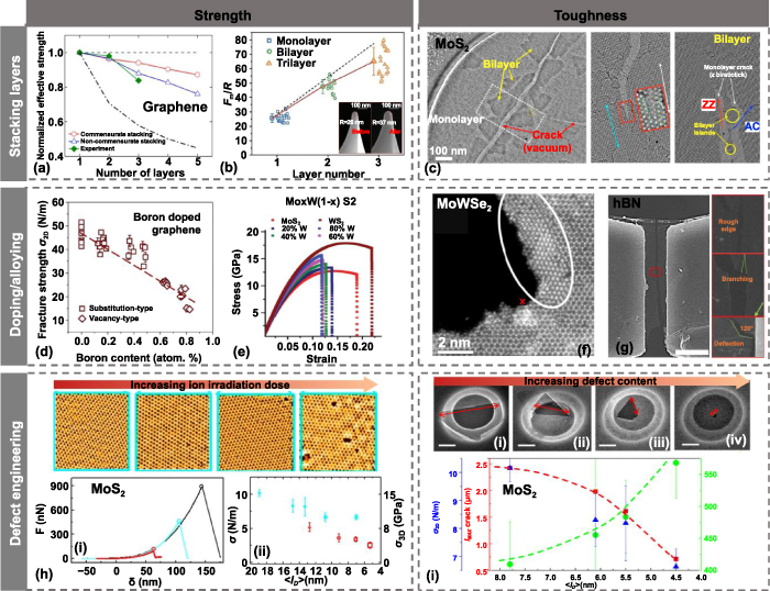
Figure 7. Representative methods to engineer the fracture properties of 2D materials. The decrease in (a) fracture strength (Reprinted with permission from [188]. Copyright (2016) American Chemical Society.) and (b) breaking force to tip radius ratio with increasing layer numbers of graphene and WS2. [219] John Wiley & Sons. (c) TEM images highlight cracks on a suspended bilayer MoS2 region and the lattice configuration of the fractured layer. Reprinted with permission from [222]. Copyright (2018) American Chemical Society. (d) Fracture strength of boron-doped graphene as a function of boron content. Reprinted from [224], Copyright (2019), with permission from Elsevier. (e) Biaxial stress versus strain curves of Mox W(1 − x)S2 alloys, showing a decreasing breaking force with increasing Mo content. [225] John Wiley & Sons. (f) STEM-HAADF image after crack propagation in MoWSe2 samples. Reprinted with permission from [226]. Copyright (2018) American Chemical Society. (g) Fracture of pre-cracked monolayer hBN and stable crack propagation. Reprinted by permission from Springer Nature Customer Service Centre GmbH: Springer Nature, Nature. [159], (c) (2021). (h) Force-deflection curves and strength as a function of defect density for ion-irradiated MoS2 monolayers as identified by STEM images. (i) Fracture strength, maximum crack length and stress intensity factor as a function of mean distance between defects in MoS2 created by controlled irradiation with increasing doses, and representative SEM images of MoS2 drumheads after rupture. Reprinted with permission from [230]. Copyright (2021) American Chemical Society.
Download figure:
Standard image High-resolution imageIn addition to the interlayer shear effect, the fracture mechanism is also responsible for the strength reduction. In particular, the failure of the monolayer and few-layer 2D membranes is mainly dominated by planar and intraplanar fracture, while thicker nanosheets feature interplanar fracture. For instance, the fracture strength of GO nanosheets was measured by in situ SEM tensile testing, giving rise to a value of 12 ± 4 GPa [8], lower than those for GO monolayers (24.7 ± 4.5 GPa [7]), yet orders of magnitude higher than that of bulk GO paper (on the level of ∼MPa [9]). This transition from the intraplanar to the interplanar fracture mechanism was verified for MoS2 samples with increasing thickness [220]. In contrast to monolayer and few-layer MoS2 (with a strength of about 30–40 GPa), the in-plane strengths of MoS2 nanosheets (tens of nanometers thick) decrease significantly to a few GPa. This degradation of strength continues to 100–250 MPa for thicker MoS2 (hundreds of nanometers).
Although the interlayer slippage tends to meditate the strength of multilayer 2D materials, it also offers a toughening mechanism by way of energy dissipation. Jang et al [221] conducted in situ mode I fracture tests under SEM imaging to study the fracture behavior of multilayer graphene. The SEM images showed asynchronous crack propagation along separate paths, causing interlayer shear deformation and slippage that lead to enhanced fracture toughness. Specifically, the fracture energy at crack initiation in the first layer was 45.5 J m−2, which increased to 98.1 and 194.0 J m−2 at the second and final crack propagation respectively.
Besides the interlayer shear-induced energy dissipation mechanism, the interplay between the stacking configuration and complex crack-tip behavior enables further control of the fracture toughness of multilayer 2D crystals. Jung et al [222] combined in situ aberration-corrected TEM and MD simulations to investigate the dynamics of crack-tip behaviors and fracture in bilayer MoS2 (figure 7(c)). The mechanical perturbation from the electron beam applied around the crack tip allows for a relatively slow propagation speed, which makes it possible to track the crack movement. It is concluded that the crack propagation in bilayer MoS2 is mainly directed by the interlayer registry. For the turbo-static stacks with arbitrary twist angle, low interlayer friction is achieved, so that the sliding between cracked and uncracked layers generates different Moiré patterns from asymmetric friction from the other layer. By comparison, in the cases of 2H (twist angle ∼60°) and 3R (twist angle ∼0°) stacks, the branched cracks are observed due to the relatively high friction resulting from the interlocking of S atoms. It is also found that the friction per unit area of the stacked bilayers is likely to decrease as the stacked area increases because local ripples and deformation facilitate interfacial sliding.
TEM observations also showed that the crack propagation in the first layer can only induce breaking in the other layers when small flaws in the second layer are located in the first crack path. Considering that cracks always initiate at the defect sites in monolayer 2D crystals due to local stress concentration under loading, extra layers may serve as a protective barrier to avoid brittle fracture of the stacked membrane [223]. Specifically, the chance of defects overlapping across the gallery space is considerably small, thus lowering the failure probability of twisted bilayer graphene than that of monolayers.
3.2.2. Doping/alloying.
Chemical doping or alloying with heteroatoms is a standard way to introduce impurities in the crystal lattice and then tailor the electronic properties of 2D materials. Since the lattice structure also determines the mechanical performance of 2D materials, some attention has been directed toward the strain engineering and fracture behavior of chemically doped graphene and TMD alloys.
Dai et al [224] examined the mechanical properties of boron-doped graphene by AFM deflection testing. While the in-plane elastic modulus appeared relatively insensitive to the chemical substitution (even at a concentration of 0.48%), the fracture strength exhibited an obvious decrease due to weaker B–C bonds (figure 7(d)). However, the failure strain and damage tolerance were greatly improved by boron substitution. Once the graphene membrane was fractured under the AFM tip, a localized failure mode rather than a catastrophic failure was observed for the boron-substituted sample, implying an increased fracture toughness. The toughening mechanism arises from the weak B–C bonds that substantially deflect propagating cracks and prevent the crack tip from spanning the entire membrane. With increasing boron content, Raman characterization showed that defects in boron-doped graphene tend to transform from substitution-type to vacancy-type. As expected, the formation of vacancies further lowered the strength, as shown in figure 7(d).
Alloying introduces a significant level of intrinsic strain in the 2D structure due to the mismatch in the lattice parameters. Ajayan and co-workers combined MD simulations and in situ Raman spectroscopy to investigate the mechanical performance of Mox W(1 − x)S2 [225]. It is observed from figure 7(e) that W substitution in MoS2 causes mechanical strengthening and increasing W content tends to decrease the failure strain for MoS2. Since hybridization induces a redistribution of the electronic charge in the region shared by the transition metal and chalcogen atoms, the W-based TMDs exhibit higher maximum strength than Mo-based TMDs. As more Mo atoms are substituted by W atoms, the overall stress values obtained for a fixed strain are larger than what MoS2 portions can withstand, so the failure strain of TMD alloy is lower than that in pure MoS2. With respect to fracture toughness, the TMD alloy exhibits a phase transition in the process zone of the crack which leads to an increase in ductility. Apte et al [226] studied the mechanical behavior of 2D MoWSe2 via in situ straining experiments conducted using a custom-built indenter. In situ local Raman frequency mapping indicated that the crack expanded mainly through MoSe2-rich regions in the alloy, due to the lower strength as discussed above. High-angle annular dark-field scanning transmission electron microscopy imaging in figure 7(f) reveals a stress buildup around the crack tip that causes an irreversible structural transformation from the 2H to 1T phase both in the MoSe2 and WSe2 domains. Crack branching and subsequent healing of a crack branch were also captured in WSe2, suggesting an increased toughness and crack propagation resistance of the alloyed 2D MoWSe2 compared to unalloyed counterparts.
More recently, the fracture toughness of single-crystal monolayer hBN has been reported by Yang et al [159], which is counterintuitively higher than that of graphene. Since the in-plane elastic modulus and fracture strength of hBN is comparable to graphene [29], its fracture behavior has long been assumed to also fall within the bounds of Griffith theory. However, the fracture toughness of hBN is measured to be one order of magnitude higher than its Griffith energy release rate. A combination of SEM and TEM visualization further reveal toughening mechanisms, including rough crack edges, crack deflections and branching, which originate from asymmetric crack tip edge elasticity and swapping during crack propagation, as shown in figure 7(g). These branched crack morphologies stand in stark contrast to graphene, which fractures by the propagation of an ideal, sharp elliptical crack [206].
3.2.3. Defect engineering/functionalization.
Defects in 2D materials have a profound effect on their mechanical properties, particularly their fracture strength and toughness. For example, the formation of grain boundaries in CVD graphene and the associated impact on the in-plane strength has remained a general concern within the community. Wei et al [227] have presented a comprehensive analysis showing a strong sensitivity of grain boundary strength with tilt angle. This behavior can be explained by the stress fields induced by pentagon–heptagon disclination dipoles that accommodate tilt rotations in graphene grain boundaries. One significant finding of this report is that well-stitched, high-angle grain boundaries in graphene only slightly degrade its strength. This was later experimentally confirmed by Lee et al [20] who report small reductions in the strength of polycrystalline graphene. Bi-crystal graphene membranes with different grain boundary misorientations have been investigated by AFM deflection testing by Rasool et al [228]. The results revealed that high-angle grain boundaries displayed a strength comparable to that of single-crystal graphene, but some weakening was observed in their low-angle counterparts. Here, the spatial distribution and density of pentagon-heptagon defects was found to play a key role in generating residual stress fields that compromised grain boundary strength. As presented in section 2.3.1, defects caused by oxygen plasma and ion irradiation not only influence the elastic properties, but also impair the in-plane strength of 2D materials. Although the in-plane elastic modulus of graphene was reported to be enhanced at an ultralow vacancy content of ∼0.2%, a reduction of 30% was measured for in-plane strength [167]. For higher defect densities a saturation of trends in mechanical properties was observed. This is consistent with a study from Gómez-Navarro and co-workers highlighting that the in-plane strength is insensitive to defect density when the mean distance between defect structures is less than 2–3 nm [229]. Similarly, ion irradiation has been employed to introduce multiatomic vacancies in MoS2 monolayers. Figure 7(h) displays typical force-displacement curves for pristine and defective MoS2 monolayers, where the breaking force drops significantly with irradiation dose. Even a density of defects below 0.2% can lead to a 40% reduction in the fracture strength [230].
Although pristine 2D graphene fractures in a brittle manner, defect engineering has been demonstrated to be an effective way to achieve a brittle-to-ductile transition of failure. For instance, a computational study from Xu et al reports that vacancy defects present as sp–sp2 rings that enable crack blocking and blunting [231]. Such toughening behavior is also enabled by Stone–Wales defects in graphene with sp–sp2–sp3 rings. Another interpretation for the improvements to ductility is that high concentrations of defects (e.g. 8%–12%) cause a crystalline-to-amorphous transition in graphene [232].
The covalent epoxide-to-ether functional group transformation via epoxide ring-opening reactions was found to confer pronounced plasticity and damage tolerance to GO monolayers [5]. The plastic deformation can be identified by deviations in the linear elastic membrane solution from the AFM force-displacement data. It can be hence envisioned that the fracture behavior of GO monolayers strongly depend on the ratio between epoxide and hydroxyl functional groups [6]. With increasing epoxide group concentration, epoxide-rich GO favors ductile failure due to a mechanochemical transformation, enabling GO to absorb energy and prevent failure through crack blunting. Thus, the failure strain and fracture toughness of GO may be tuned by controlling the surface chemistry.
Similar brittle-to-ductile transitions were also observed in the vacancy-defective MoS2 under Ar+ irradiation and Ga+ bombardment [230], as shown in figure 7(i). By inducing local ruptures through AFM deflection testing, the crack length and corresponding stress intensity factor were measured as a function of the vacancies, which is related to defect density. Indeed, at vacancy densities as low as ∼0.15%, the crack propagation length during fracture instability was found to decrease from several microns to tens of nanometers, giving rise to a higher toughness. Furthermore, by in situ TEM observation of the fracture process of monolayer MoS2, it was also demonstrated that the increasing vacancy density shifted the fracture mechanisms from brittle to ductile by the migration of vacancies into defect networks within the crack-tip strain field [233].
3.3. Atomistic simulations of in-plane inelastic behavior in 2D materials
The inherent length- (sub-nm) and timescales (fs) of atomistic simulations present a powerful pathway to examine the in-plane inelastic properties of 2D materials. In this regard, these methods offer a platform to examine the atomic-scale features of plasticity in 2D materials at resolutions inaccessible to experiments. In this section, atomistic simulations of the inelastic behavior of 2D materials are overviewed. This discussion will overview aspects of in-plane strength, with a focus on defect mechanics and fracture toughening mechanisms.
3.3.1. Defect mechanics in 2D materials.
The earliest atomistic studies of defect behaviors in 2D materials are naturally found in the graphitic systems, which tracks with the experimental chronology. A number of early insightful studies on the detrimental role of topological defects in the degradation of the in-plane strength of monolayer materials have been reported in the literature [234, 235]. Graphene presents an interesting benchmark material, where a number of counterintuitive defect mechanics findings have been reported. For instance, MD-based studies have identified low-energy topological structures, such as the Stone–Wales defect [236] and specific configurations of tilt grain boundaries [227, 237], which seem not to cause weakening. In the latter case (e.g. grain boundary studies) Grantab et al [237] report intragranular fracture by cleavage of pristine carbon–carbon bonds as the failure pathway for some types of graphene tilt boundaries (as opposed to bond cleavage at the boundary). However, caution must be taken when interpreting defect tolerance based on these reports due to the extremely high strain rates inherent to MD mechanical simulations, which restrict the operation of thermal activation in defect mechanics. Indeed, many of these findings of defect insensitivity (e.g. strength of grain boundaries exceeding pristine graphene) have not been replicated by experimental studies [20]. In addition to these early defect studies, later works have systematically mapped the defect mechanics of graphene, which includes studies of vacancy densities [231], the strength of grain boundaries under arbitrary in-plane tension [238], flaw sensitivity in nanocrystalline graphene [239], the strength of curvilinear grain boundaries [240], and the temperature- and strain-rate dependencies of fracture strengths in pre-cracked graphene [241]. Beyond graphene, atomistic studies of defect mechanics have been reported for several systems, including hBN [242–244], TMDs [233, 245–247], and phosphorene [248].
In addition to studies of the baseline in-plane mechanical properties of defective 2D materials, atomistic simulations have revealed a number of interesting plasticity mechanisms that offer pathways for toughening and defect tolerance. For instance, Espinosa and co-workers report a stress-induced epoxide-to-ether transformation of functional groups in GO that lead to significant toughening behavior, as mentioned in the previous section [5, 6]. In addition to bonding transformations, more recent atomistic studies have focused on structural phase transformations in response to applied mechanical stresses. Gao and co-workers have analyzed stress-modulated phase transformations in MoTe2 monolayers using the finite deformation nudged elastic band method [249, 250]. Similar phase transformations have been reported in nanoindentation simulations of MoS2 [251]. In addition to phase transformations, deformation twinning has been observed in DFTB simulations of phosphorene [252]. These reports of unconventional plasticity mechanisms in 2D systems highlight pathways to improve the toughness of this nominally brittle class of materials.
3.3.2. Fracture toughening mechanisms.
In addition to the discovery of atomic-scale defect mechanics, computational studies have been extensively used to study fracture toughening mechanisms in 2D materials. Indeed, the literature offers several key reports on intrinsic and extrinsic toughening mechanisms for a variety of 2D systems. For instance, as mentioned previously, Yang et al [159] report a novel intrinsic toughening mechanism in hBN based on MD studies of crack growth. In this mechanism, the asymmetry of the stress state at cleaved B and N bonds along a crack front activates a Mode II fracture, which leads to crack branching. The end result of this toughening mechanism is a fracture toughness that exceeds the Griffith criteria. Interestingly, it is the compound chemistry of hBN that enables this unusual fracture behavior, which is inherently unavailable to pure substances such as graphene.
While pristine graphene remains prized for its record-breaking in-plane properties, any practical application of graphene must reconcile its excellent strength with its poor fracture toughness. Recognition of this practicality has led the computational mechanics community to embrace a number of creative solutions to graphene's fracture toughness dilemma. Crack bridging presents one strategy to toughen graphene. In this regard, Hacopian et al [11] studied graphene decorated with carbon nanotubes, which demonstrated crack deflection and toughening behavior. In addition to crack bridging reinforcements, a recent study from Sandoz-Rosado et al [253] presents a relatively unique approach to toughening graphene. In this work, the authors propose a 2D polymer 'graphylene', which possesses ethylene bridge units positioned between C6 rings in a monolayer configuration. MD simulations of fracture in this system measure an energy release rate double to that of pristine graphene, which is accompanied by delocalized failure, and crack bridging and branching mechanisms.
In addition to graphene, the fracture properties of GO have received considerable attention. In contrast to pristine graphene, which relies on relatively weak vdW layers to interact with crack bridging materials, the surface chemistry of GO offers much stronger bonding to anchor reinforcement. The extrinsic toughening of cracks in GO by polymer reinforcement has been studied by Najafi et al [254], and Zhang et al [255]. In the latter study, five different polymers were screened for their extrinsic toughening on epoxide-rich GO. A key finding of this work is that polymers that can form donor and acceptor hydrogen bonds exhibit the strongest crack bridging. While these computational studies have highlighted a number of potential pathways to toughen the nominally brittle fracture behavior of 2D systems, in many cases some practical issues still require resolution. Namely, scale-up of 2D-polymer composite plies requires methods to manipulate and place monolayers and polymers in alternating stacks. This challenge can be viewed within the larger issue of scalable heterostructure manufacturing, of which the community is familiar.
4. Fatigue
Mechanical failures due to fatigue account for 80%–90% of bulk material failures [256]. Furthermore, fatigue fracture by dynamic loading typically occurs at stresses significantly lower than quasi-static strengths, which underscores the need to capture the fatigue properties of emerging 2D materials. Sub-critical, cyclic loadings are realized in 2D materials in many of their target applications, such as flexible electronics [257] and bio-nano interfaces [258]. To develop functional 2D materials-based devices with long-term stability, a comprehensive understanding of fatigue behavior is therefore required. However, experimental investigations of the fatigue of 2D materials are not trivial due to the lack of standardized techniques and progress has been lagging until recently.
MEMS-based testing platforms [259] like a digital micromirror device [260] have emerged as powerful and versatile tools to investigate fatigue properties of various nanostructures [259, 261] including nanowires [262], nanotubes [263], and thin films [264]. For instance, a MEMS-based tensile testing setup [264] was developed to perform quantitative in situ fatigue testing under TEM, where both specimen elongation and applied force could be measured with built-in capacitive sensors. This setup was used to study the nanoscale fatigue cracks of ultrathin nanocrystalline Au films under tensile cyclic loading and ratcheting behavior was observed in near stress-controlled conditions. Some other fatigue testing platforms have also been developed for fatigue studies of nanomaterials. For example, the PTP device for in situ TEM mechanical testing mentioned above for modulus and fracture toughness measurement [265] has also been applied to fatigue studies of nanowires [266]. However, within the context of 2D materials testing, a unique challenge emerges from the difficulties in applying uniform loadings to 2D surfaces. Fatigue testing systems have also been developed for thin films, like the micro-force test system used to study the length-scale effect on the dynamic tensile fatigue of thin metallic films; however, these testing methods are limited to micro/submicron scales [267]. The inherent properties and difficulties in materials handling present several challenges in probing the fatigue behavior of 2D materials. Namely, the high intrinsic strength of many 2D materials suggests that these materials may survive billions of load cycles until fracture, which requires high loading frequency to make testing manageable. In addition, 2D materials are usually exfoliated on substrates, which creates non-trivial challenges in establishing a uniform, dynamic loading configuration. These factors may contribute to the fact that the fatigue testing methods for 2D materials were not reported until recently [268–272]. AFM-based cyclic deflection tests coupled with computational modeling were first applied to study the fatigue behaviors of free-standing 2D materials (both dynamic and static). Direct cyclic tensile tests followed these earlier AFM-based works to study the interfacial fatigue in substrate-supported 2D materials. In this section, recent advances in studies of fatigue behaviors of 2D materials will be reviewed in detail. The methodologies developed to characterize the fatigue of 2D materials and interfaces will be introduced, followed by exemplary fatigue studies of graphene, GO and TMDs.
4.1. Methodology
4.1.1. AFM-based fatigue measurement.
Probing the fatigue behaviors of 2D materials by AFM-based membrane deflection methods was first introduced by Cui et al [268]. In these experiments, a 2D material flake was suspended over a perforated silicon wafer. Two load-controlled fatigue configurations were performed: cyclic membrane deflection at a predefined frequency and amplitude for dynamic fatigue, and constant loading under contact with the AFM tip for static fatigue (figure 8(a)). In dynamic fatigue, by varying the drive amplitude and frequency (assuming the tip and the film are always in contact), the film suffers fatigue failure at different mean stress levels. When fatigue failure occurs in either configuration (dynamic or static), an abrupt change in the amplitude signal can be observed. The number of dynamic loading cycles or the amount of time at a certain load that 2D materials can sustain before failure is recognized as the fatigue 'life' of 2D materials.

Figure 8. Schematics of experimental setups for the characterizations of the fatigue behaviors of 2D materials. (a) AFM-based fatigue tests: a suspended 2D material is cyclically deflected under an AFM tip until failure. Reprinted by permission from Springer Nature Customer Service Centre GmbH: Springer Nature, Nat. Mater [268]. (c) 2020. (b) Interfacial fatigue testing for 2D materials via direct cyclic tension: a polymer substrate with a 2D material transferred atop is loaded cyclically in situ optical microscopy to characterize the interfacial fatigue between the 2D material and the polymer substrate. From [269]. Reprinted with permission from AAAS.
Download figure:
Standard image High-resolution image4.1.2. Cyclic tensile loading for the measurement of interfacial fatigue between 2D materials and a substrate.
In the interfacial fatigue experiment [269], as illustrated in figure 8(b), a 2D film is exfoliated onto a stretchable substrate (e.g. PDMS), and the substrate is subsequently subjected to uniaxial cyclic loading. By controlling the uniaxial deformation amplitude, the sample film is loaded under different strain rates. The optical microscope records the damage occurrence and propagation process from the top view. Here, the fatigue resistance of the materials is characterized by the crack growth rate da/dN as a function of fatigue cycle N, where a is the crack length. The crack length is defined as a = L − ΔL, where L is the total length of the sample film and ΔL is the undamaged length.
4.2. Fatigue behavior of 2D materials
4.2.1. Graphene.
Applying the methodology discussed above in figure 8(a), the fatigue life of monolayer and few-layer mechanically exfoliated graphene withstands more than 109 cycles at a mean stress of 71 GPa and a stress amplitude of ±5.6 GPa (figure 9(a)), which is a record-breaking value. Here, the Fdc /Ffracture–N (cycle) curve is used to illustrate the fatigue life of 2D materials, where Fdc is the applied static force, Ffracture is the averaged quasi-static fracture force. This approach is analogous to the S(stress)—N curve in conventional fatigue theory. The probability of survival was given as a two-parameter Weibull distribution:
Figure 9. Fatigue behavior of graphene. (a) Fdc/Ffracture–N curve of graphene with an oscillation amplitude of 5 nm. (b) Probability of survival for graphene. (c) Graphene amplitude and static deflection during fatigue loading. An abrupt change indicates the onset of fatigue failure. The inset image shows the sample condition before and after the failure. Reprinted by permission from Springer Nature Customer Service Centre GmbH: Springer Nature, Nat. Mater [268]. (c) 2020. (d) Real-time optical images showing the propagation of buckling zone under various fatigue cycles: L is the total length of the sample film and ΔL is the length of the undamaged area. (e) Mixed-mode fatigue fracture comprised of mode I fracture under monotonic loading at low tensile strain rates, mode II fracture caused by in-plane shear, and mode III fracture caused by out-of-plane tearing. From [269]. Reprinted with permission from AAAS.
Download figure:
Standard image High-resolution imagewhere m is the Weibull modulus,  is the nominal ratio. Usually, a larger m indicates that failure is less sensitive to defects. As shown in figure 9(b), m is the largest for the static loading case and smallest for the graphene that survived 109 cycles of deflections, which indicates that graphene is less sensitive to defects under quasi-static loading than under cyclic loading.
Based on the AFM data, monolayer graphene samples all failed catastrophically or remained intact after billions of cycles of loading [268]. As shown in figure 9(c), while the stress level near the fracture area was constant up until the point of failure, AFM topographic imaging showed the fatigue failure in monolayer graphene was global and catastrophic without progressive damage. That is, once nucleated, critical fatigue cracks propagate and fail graphene films without arresting. This stands in contrast to GO, which exhibits a stress-induced epoxide-to-ether transformation as a toughening mechanism [5]. MD simulations also revealed that longer times were needed to initiate bond breaking. Yet, upon nucleation of defects, fracture proceeded immediately via bond reconfiguration in the process zone of the defect. An important interpretation from this result is that conventional macroscopic fatigue phenomena might not apply to graphene monolayers.
Shear stress induced fatigue of graphene via vdW interactions was also investigated by the same group [271]. Interfacial fatigue between graphene and a PDMS substrate was measured by cyclic uniaxial loading under optical imaging, as described in section 4.1.2. As shown in figure 9(d), the varied elastic properties of graphene and PDMS create shear tractions at the interface. As the number of loading/unloading cycles increases, periodic wrinkles and local buckling-induced delamination were observed (black lines are buckling features and white lines are folds) and propagated inward parallel to the loading direction. The wrinkles transitioned to folds with an increased compressive stress on graphene during unloading. By analyzing the relationship between the change in interfacial strain intensity factor and damage propagation rate (equation (10)), it was found that the interfacial fatigue damage at the graphene-PDMS interfaces can be described by a modified Paris' law, suggesting the crack propagation is at a mid-growth rate:
where c and m are fitting parameters,  is the change in interfacial strain intensity factor, and da/dN is the crack propagation rate. In classical fatigue, the fatigue crack propagation rate increases with growing cycles (m > 0) until eventual fracture. However, the interfacial fatigue damage propagation exhibits a reverse trend (m < 0). The authors attributed this to the drastically different fatigue damage mechanisms. Buckling features and folds were formed in the early loading cycles, which resulted in a smaller middle contact region between graphene and substrate. The existing buckling zone was more energetically favored to dissipate energy from later cycles, which led to a decrease in the crack propagation rate.
In addition to the fatigue damage propagation, cyclic loading through vdW contact caused mixed-mode fatigue fracture in pristine graphene through a combined in-plane shear and out-of-plane tearing mechanism (figure 9(e)). As the number of loading cycles increased, interfacial instabilities evolved into intersection folds on the graphene surface and divided the graphene flake into small islands. Subsequently, the deformation on the surface became incoherent at the fold boundaries, where the shear stress cannot effectively be transferred and gradually formed stress concentrations along the folds, which eventually resulted in cracking. In addition, tearing was also observed as shown in figure 9(e). The tearing process propagated quickly, and the arrest of tearing of the graphene ribbon was observed along fold boundaries. As cyclic loading continuously inputs strain energy into the graphene from the PDMS, the torn graphene has to further separate itself from the main body (e.g. by increasing the tear width) to release the energy.
4.2.2. GO and graphene composites.
Using the same protocol described in section 4.1.1, fatigue behaviors of GO were also investigated. While the average fatigue life cycle of GO was found to be approximately an order of magnitude lower than that of graphene [268] (figures 9(a) and 10(a)), functional groups in GO imparted a local and progressive fatigue damage mechanism, which is attributed to the unique crack-arresting behaviors of GO [205]. The mechanistic difference in fatigue behaviors between graphene and GO indicates that functionalization can potentially be a route for tuning the fatigue life of 2D materials [270]. The authors also performed detailed MD simulations to investigate the relationship between fatigue life and the degree of functionalization. They report that the effect of functionalization on the fatigue life of GO is not monotonic; and critical degrees of functionalization exist such that the GO is neither too defective (poor in strength) nor too graphene-like (abrupt fatigue fracture), to exhibit a balanced fatigue life and fracture resistance.

Figure 10. Fatigue lives of representative 2D materials. (a) Fdc /Ffracture –N curve of GO: there is at least one order of magnitude difference in fatigue life between fewer-layer GO and thick GO due to the presence of critical defects. Reprinted by permission from Springer Nature Customer Service Centre GmbH: Springer Nature, Nat. Mater [268]. (c) 2020. (b) Fdc /Ffracture –N curve of CVD graphene and a-Al2O3@G films. Reprinted with permission from [271]. Copyright (2021) American Chemical Society. (c) Experimental results on the mechanical reliability of monolayer MoS2 and WSe2 under static fatigue loading. Reprinted from [272], Copyright (2022), with permission from Elsevier.
Download figure:
Standard image High-resolution imageIn addition to graphene and GO, fatigue behaviors of graphene-based nanocomposites were also investigated [271]. The fatigue life of ultrathin alumina-graphene laminates with varied alumina thicknesses was characterized using the same method described in section 4.1.1. As figure 10(b) shows, when alumina is extremely thin (under ∼10 ALD cycles), the fatigue life of the composite can reach up to that of pure graphene (a billion cycles) even at 80% of the average fracture forces. Yet, thicker alumina layers lower the fatigue life of the composite when the composite is thinner than 16.5 nm. When the film is too thick, the testing method may not work effectively, because the setup may not provide enough force to cause the material to undergo fatigue fracture. Furthermore, the underlying assumption of the mechanics model—that elastic strain energy is stored by plane stretching but not bending during indentation—will be violated.
4.2.3. TMDs.
Fatigue behaviors of some TMDs have also been investigated recently. Using the same AFM-based approach (section 4.1.1), the static fatigue of monolayer MoS2 and WSe2 were studied [272]. To determine their mechanical reliability under static fatigue loading conditions, the failure probability was analyzed with respect to the dwell time. As reported in this study, the failure probability P under long-term loading can be described by a two-parameter Weibull distribution as shown below:
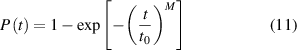
where t0 is the characteristic lifetime, and M is the Weibull modulus (both are fitting parameters). The value of M indicates the consistency level of the measured lifetime. Weibull plots of fatigue failure probability of monolayer MoS2 and WSe2 at different static loading levels are shown in figure 10(c). Some key insights from the plots include that even at the same applied force, the lifetime can span across several orders of magnitude and the static fatigue lifetime is scattered across a wider range (larger M) when the applied force is increased.
To better understand the low mechanical reliability, MD simulations were performed to study the effects of thermal fluctuations, defect type, defect configuration and defect density using MoS2, and its most dominant defect sulphur vacancy, as a representative system. It was revealed that higher temperature can result in a higher failure probability and larger statistical scatter under static fatigue. Furthermore, it was shown that reliability is also strongly governed by the defect distributions and defect interactions, despite the expectation that static fatigue life is more scattered at increasing defect numbers and densities.
5. Interfacial shear and frictional properties
Interfacial shear properties—that is, the deviatoric aspects of the out-of-plane mechanical response of 2D materials—are of inherent interest to the mechanics community. For instance, when compared to in-plane properties, the interfacial cohesion of 2D materials is generally very weak, which is a key requirement of exfoliation-based monolayer processing routes. Conversely, structural applications intuitively require stronger interlayer bonding between 2D layers for load transfer purposes. These opposing characteristics remain an open challenge in the large-scale synthesis and scale-up of 2D material systems. This section provides a review of the library of 2D materials for which the interfacial properties have been measured and methods to increase, decrease, and tune interfacial properties are discussed. Here, we distinguish two manners of related interfacial properties: frictional and interfacial shear measurements. The former category refers to tribological testing where the forces at surface asperity contacts are quantified and used to extract friction coefficients. The latter property focuses on the traction-sliding relationships and the stresses required to cause slippage in subsurface structures. Although related to friction, this measurement assumes conformal contact (as opposed to asperity) between 2D material layers and substrates. This section will also detail the different experimental approaches that can be leveraged to collect these measurements.
5.1. Surface friction of 2D materials
5.1.1. FFM measurements of 2D materials.
The friction force is typically measured by FFM with an AFM tip sliding on the surface in contact mode at a constant normal load. For instance, Filleter et al [273] have observed atomic stick-slip friction by FFM on graphene epitaxially grown on a SiC substrate. Lee et al [274] further systematically studied the thickness dependence of friction for different 2D materials, including graphene, MoS2, NbSe2, and hBN, exfoliated onto a silicon oxide substrate. The FFM measurements showed that for all four 2D materials the friction monotonically decreased with increasing layer numbers.
Conversely, a recent tribological study of MXenes [275] presented an opposing phenomenon, where a thickness independence is demonstrated across all normal loads for few-layer Ti3C2Tx . This result arises from the strong interlayer coupling between different termination states of Ti3C2Tx , with binding strengths 2–4 times higher than that of graphene and MoS2. Indeed, the surface termination chemistry of 2D MXenes enables a tunable nanoscale lubricity, which can be engineered to produce even lower friction forces (up to 57% decrease) by the reduction of hydroxyl termination through annealing (figure 11(a)). Furthermore, MXenes have demonstrated long-term lubricity, with one study reporting sustained lubricating abilities for up to 54 d after removal from solution, and despite structural changes upon drying (figure 11(b)).
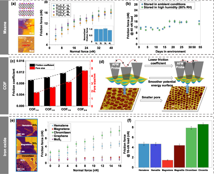
Figure 11. Frictional behaviors of representative 2D materials. (a) Friction force for as-deposited and annealed MXene flakes. (b) Friction force at 40 nN load for MXenes 2D flakes drop-cast on day 0 and stored under ambient conditions (25% RH) and high humidity (80% RH). Reprinted with permission from [275]. Copyright (2022) American Chemical Society. (c) Friction coefficients of COFs with varied pore sizes. (d) Nanotribological mechanism model of surface COFs. Reprinted with permission from [276]. Copyright (2022) American Chemical Society. (e) Friction force of the three non-vdW iron oxide 2D materials and two vdW materials. (f) Friction force at maximum load (16 nN) for the 2D and 3D forms of the non-vdW iron oxides. From [280]. Reprinted with permission from AAAS.
Download figure:
Standard image High-resolution imageRecently, FFM measurements have been expanded to other members of the TMD family, where friction behaviors were compared among MoS2, MoSe2, and MoTe2 to understand the effect of the chalcogen on the tribological behavior [277]. The experimental results show that MoS2 has the highest friction coefficient among these materials and MoTe2 has the lowest. After excluding potential factors such as contact size, out-of-plane deformation, and maximum energy barriers (peak-to-valley energy in tip-sample potential energy surface), the observed trend was explained by the interplay between energy barriers and lattice constants that differed depending on the chalcogen. While the corrugation amplitudes of the energy landscapes are similar for all three materials, the larger lattice spacings of MoSe2 and MoTe2 permit the tip to slide more easily across correspondingly wider saddle points, which progressively reduces the friction force.
The change in material composition also affects the interfacial interactions between the AFM tip and the sliding surface. This is evidenced by the nanotribological study of monolayer Mox W1 − x S2 [278] alloy, where the friction is found to decrease monotonically from MoS2 to WS2 region with the reduced molybdenum concentration. While MoS2 and WS2 are reported to have almost the same crystallographic structure and small differences in the lattice constants, the interfacial interactions are considered the major reasons for the spatial variations in friction between the material domains. It is concluded that the decreasing number and total energy of the excited phonons, along with the weakened interfacial interaction, lead to decreased dissipated energy and reduced friction force. Another study by Yadav et al [279] investigated the tribological behavior of metal counter-surfaces (e.g. titanium and copper) with 2D materials by using customized AFM probes. It was found that both the metals underwent surface oxidation, giving rise to TiO2 (rutile titanium dioxide) and CuO (cupric oxide) which were mostly chemisorbed along the interface with 2D materials. These oxides both exhibited higher friction force and adhesion on graphene than on MoS2, mainly due to more homogenous interfacial charge distribution and lower surface energy variation. The nanotribological behavior was also investigated on organic 2D materials, where COFs [276] are synthesized on the surface of HOPG. It is found that the coefficient of friction of surface COFs is positively correlated with the pore sizes of honeycomb networks, as shown in figure 11(c). This is because for the surface COFs with 2D porous structures, the potential energy surfaces will fluctuate with the alternation of the backbone and pore of surface COFs. Smaller pores with a smoother potential energy surface give rise to a lower energy barrier for the probe to overcome during the sliding process, thus endowing fine-pore COFs with a lower coefficient of friction (figure 11(d)). In addition, the branched chains create extra interaction with the AFM probe, resulting in increased frictional resistance to relative movement. Note that, the porous structures of COFs make them good candidates to be host templates, and assembled host–guest systems can display higher friction since the assembly structure of the guest molecules would be perturbed during the friction process and bring additional slip energy barriers.
More recently, Serles et al [280] examined the friction behavior of non-vdW materials such as magnetene, which is a 2D iron oxide. It is demonstrated that the lubricating characteristics that are typical of graphene and other vdW 2D materials can be achieved in magnetene as well, as presented in figure 11(e). Such low-friction behavior of magnetene is markedly different from the other two non-vdW materials (hematene and chromitene) as well as its bulk form (magnetite) (figure 11(f)). As magnetene exhibits a shear constant that is statistically similar to chromitene while the friction behavior is the contrary, this implies that the lattice structure and subsurface shear are not dominant mechanisms for the lubricity of 2D non-vdW materials. In contrast to the vdW bonding governed superlubricity, three main mechanisms have been proposed, including 2D confinement effects of minimized potential energy surface corrugation, lowered valence states reducing surface adsorbates, and forbidden low-damping phonon modes, which all contribute to the low friction of magnetene.
The common friction mechanisms of various 2D materials, including puckering effect, electron–phonon coupling, contact quality, have been comprehensively introduced in existing reviews [186, 281]. Recently, Rejhon et al [282] devised a modulated nano-shear method with sub-Angstrom AFM tip indentation and for the first time measured the interfacial transverse shear modulus of the top atomic layer against the underlying materials. By tuning the film thickness, stacking order and surface chemistry of substrates, they demonstrated that the interfacial shear modulus and 2D layer–substrate interactions are two key parameters dominating the friction behavior of 2D materials. A general reciprocal relationship between the friction force and interfacial shear modulus was established for the investigated graphitic structures, representing a pathway to control and predict atomic sliding friction for supported 2D materials.
5.1.2. External factors influencing the friction performance.
Current tribological studies of emerging 2D materials, as discussed above, demonstrate the key role of microstructure on the surface friction behavior. Intrinsic factors including defects, functionalization and interfacial commensurability have been overviewed in detail in previous reviews [281, 283]. Beyond these parameters, as is typical with surface-mediated phenomena, friction is susceptible to the influence of the external environment. Environmental considerations are of practical importance, as exposure to a range of conditions is inevitable in many engineering applications.
5.1.2.1. Strain effect.
Strain engineering [284]—that is, the application of mechanical strain to modify functional behavior—offers a pathway to expand the properties of 2D materials. The effect of strain on the friction performance of 2D materials was noted in a recent work by Zhang et al [285], where in-plane strain was created and controlled through a pressurized graphene bubble (figure 12(a)). Friction measurements showed that the coefficient of friction reduced to nearly 0.001 for suspended graphene under an in-plane biaxial strain of 0.6%, reaching a superlubric state. Since the in-plane strain effectively modulates the flexibility of graphene, the roughness of atomic-scale contact at the sliding interface was decreased to regulate the friction behavior.

Figure 12. Environmental and physical effects on the frictional behaviors of 2D materials. (a) The friction coefficient of graphene with different strains created by pressurized graphene bubbles. Reproduced with permission from [285]. (b) Evolution of graphene mean friction with graphene relative strain in five cycles, showing two different regimes. Reprinted with permission from [286]. Copyright (2022) American Chemical Society. (c) Schematic diagram of electric-carrying friction of local functionalized graphene. Reproduced from [289] with permission from the Royal Society of Chemistry. (d) Average friction as a function of tip voltages. Reprinted with permission from [290]. Copyright (2020) American Chemical Society. (e) Friction as a function of normal load for humid ambient air and dry nitrogen environment at different temperatures. Reprinted with permission from [294]. Copyright (2010) American Chemical Society. (f) Variation of friction with load acquired on unheated and heated samples. The insets are lateral force line profiles corresponding to the load/friction force points indicated by the black dashed arrow. Reprinted from [295], with the permission of AIP Publishing. (g) Comparison of the average friction force between beaded and sharp SiO2 tip against GO sample and beaded SiO2 tip against graphene for different normal loads as a function of relative humidity. (h) Schematics of the humidity-controlled friction mechanism of GO. Reprinted with permission from [297]. Copyright (2018) American Chemical Society.
Download figure:
Standard image High-resolution imageBy depositing graphene onto a stretchable substrate, the frictional characteristics of supported graphene under a wide range of strain are examined with an in situ tensile loading platform [286]. Analogous to the suspended system, the friction of supported graphene tends to decrease with increasing strain, yet shows two distinct stages with considerably different strain dependences (figure 12(b)). Combining AFM phase imaging with lateral force imaging, the unique friction behavior is attributed to the transition between two friction modulation modes, e.g. contact-quality-dominated friction and puckering-dominated friction, depending on the adherence state of the graphene/substrate interface.
In contrast to graphene, a reversal of the strain effect was observed in MoS2 nanoblisters [287], showing an increased friction with an elevated strain level. In particular, as the height to radius (h/r) ratios of MoS2 nanoblisters increase, the amplitude of stick-slip curves was found to increase, accompanied by a rise in the local peak friction force. Additionally, the difference between trace and retrace stick-slip curves increase as the h/r ratios increase, indicating that more energy dissipation is required to move the tip during the sliding process. Interestingly, both nanoblisters and microbubbles (as discussed above) provide biaxially in-plane strain fields, but the friction behaviors of MoS2 and graphene exhibit opposite trends in friction behavior. The underlying physical mechanism for this disparity may arise from differences in bubble h/r ratios across different scales. Another possible reason lies in the presence of confined water within the MoS2 nanoblisters, where the encapsulated water may interact with MoS2, resulting in different friction performance from that on gas-pressurized microbubbles.
5.1.2.2. Electrical effect.
The electric field may have an influence on the phonon vibration, electron motion or electrostatic force during the sliding process, which can modulate the friction behavior of 2D materials [288]. Conductive AFM is a commonly used method to construct a relatively stable electric field between the cantilever and 2D materials. Using this approach, Lang et al [289] found that the application of a negatively biased voltage could cause electrochemical functionalization of graphene in the ambient atmosphere. By tuning the voltages of tips, the friction force was increased by more than eight times, as a result of increased water bridge (meniscus force) and the polarization of functionalized graphene (electrostatic force) induced by the electrical field (figure 12(c)). Later, they used [290] the same method to investigate the effect of positive voltage on the friction of graphene. In contrast to negative voltages, the structure of graphene was unchanged under positive voltages and friction remained low (figure 12(d)). The distinct response of the friction of graphene to the positive and negative bias stems from the work function difference and the different role of water molecules between tip and sample. The electrical field induced increase of friction is also presented for hBN [291], where the electrostatic attraction generated by the charging effect leads to a change in the normal load, thereby altering the friction and adhesion of hBN.
In contrast to graphene and hBN, the negative electric field tends to reduce the friction force of monolayer MoS2 [291] by ∼5 times. The shift and transfer of an electron between MoS2 and SiO2/Si substrate leads to electronically tight binding at the interface, which suppresses the formation of puckering and restricts the evolution of contact quality to obtain an ultra-low friction state. More recently, Song et al [292] provide a deeper examination of the tuning mechanisms of friction by an electric field. In contrast to the existing mechanisms related to the atomic configurations and electrostatic forces, the investigators concentrated on the interfacial electronic properties between the AFM tip and 2D materials. It was documented that the modulation of friction by an electric field was achieved by the fluctuation of electronic properties, in terms of electric-field-induced electron density redistribution and current-induced electron transfer.
5.1.2.3. Thermal effect.
With the exploration of friction origins at the atomic scale, various fundamental mechanisms, such as electron–phonon coupling and out-of-plane puckering, have been proposed, which are strongly modulated by temperature. Hence, temperature has been deemed as an important parameter influencing the frictional properties of 2D materials. Zhang et al [293] found that the friction force of graphene on silica substrates increases by four-fold with increasing temperatures from 288 K to 388 K. This increase is attributed to large corrugations in graphene at higher temperatures, which hinders the sliding of a tip on its surface. Using a silicon AFM probe equipped with an in situ solid-state heater, Carpick and co-workers [294] demonstrated the delicate control of single-asperity friction via local nanoscale heating. Specifically, heating was found to increase the friction force by a factor of 4 in air at a relative humidity of 30%, which is attributed to thermally assisted formation of capillary bridges between the tip and substrate in ambient atmosphere (figure 12(e)). By contrast, in dry nitrogen the friction decreased by ∼40%, resulting from the thermally assisted sliding that suppressed the stick-slip of the tip and made it easier to overcome the energy barrier. Such 'thermolubricity' behavior has also been reported previously on HOPG. The effect of heating on surface contamination and friction properties of trilayer graphene was investigated by Egbert and co-workers [295]. It was noted that heating the sample at 800 °C for 3 h in the ultra-high vacuum chamber likely removed or reduced the amount of contamination of the surface to undetectable levels. The cleaner surface favored lower friction forces, lower pull-off forces, as well as a weaker dependence of friction on load. Moreover, the observed hysteresis in the friction forces was greatly suppressed, which may be a result of removal of meniscus at the tip–sample contact, as depicted in figure 12(f).
5.1.2.4. Humidity effect.
Early studies have shown no appreciable difference in the friction performance of graphene when the experiments are conducted in vacuum, dry nitrogen and humid air conditions [274, 296]. The insensitivity to humidity is ascribed to the inert and hydrophobic nature of graphene. However, since most friction measurements are performed at ambient environments, it has been gradually realized that long-time exposure to water would change the surface chemistry and hence friction properties of 2D materials.
Recently, Arif et al [297] carried out a series of humidity-control FFM measurements on graphene and GO with a beaded tip, revealing the effect of water on their tribological behavior. In particular, when performing the friction measurements on graphene using silicon oxide tip, the behavior is dominated by water adsorption at the low/intermediary humidity regime (5%–50% RH), and in the high humidity regime (50%–70% RH) by meniscus/capillary condensation. Overall, the humidity dependence of friction is not that significant. In stark contrast, GO presents an increased trend of friction force with relative humidity, as shown in figure 12(g). Water molecules are found to easily intercalate between GO layers, which increases the film thickness by up to 100% as well as inducing higher roughness (figure 12(h)). Furthermore, the increase of humidity also causes the formation of a water meniscus at the tip/sample contact. Since the hydrophilic surface of GO forms stronger bonding meniscus compared to graphene, higher energy is required to slide the bead. In comparison to FFM measurements with a sharp tip, an increase in wearing behavior was observed for GO even at low humidity.
In contrast to graphene, MoS2 [298] is more sensitive to the presence of water even without water intercalation between the layers, because of the oxidation of MoS2 edge or defect sites when exposed to the humid environment. MoS2 was observed to retain its low friction and adhesion behavior only at low humidity and in a narrower range (RH 5%–20%), which is dominated by water absorption instead of intercalation. More recently, the humidity-dependent tribological behavior of MoS2 on a custom-fabricated 440C-steel counter-surface has been investigated [299]. The presence of oxides on the 440C-steel counter-surface is found to create stronger chemical bonding with MoS2, leading to higher friction. Notably, water was observed to reduce friction for such chemically interacting interfaces, where adsorbed water molecules act as a temporary lubricating film to suppress the interfacial chemical interaction.
Vilhena et al [300] performed FFM measurements on graphene when it was completely immersed in water. Despite the influence of the aqueous environment, high-resolution friction images showing clear atomic-scale stick–slip behavior were repeatedly obtained. When these results were combined with MD simulations, it was revealed that water only played a purely stochastic role in frictional sliding after the hydration layer that had formed at the graphene/water interface was broken.
5.2. Interfacial shear properties between 2D materials
5.2.1. Tip-based interlayer measurements.
At the nanoscale, AFM-based friction testing provides a facile avenue for characterizing the superlubricity between atomically clean surfaces in 2D materials. Graphene-coated AFM tips provide one example of this characterization pathway, and can be produced by either mechanical transfer or CVD methods. For example, Liu et al [301] fabricated a graphene-coated AFM probe by metal-catalyst-free CVD, to measure sliding behavior in multiple asperity contact on graphite. The low friction coefficient of 0.003 was obtained at arbitrary sliding orientations, because graphene nanograins oriented randomly at asperities invariably lead to incommensurate contact (figure 13(a)). That is, orientation variations preclude perfect commensurate contact and the associated stick–slip behavior. The result of this incommensurate contact is smooth sliding and reduced energy dissipation. Multi-asperity contact can also be achieved in the pre-sliding process on graphite, during which graphene nanoflakes are transferred onto the AFM probe via tribointeractions [302]. The friction coefficient was found to decrease to approximately 0.0003, which arises from the extremely weak interaction and easy sliding between the multiple transferred graphene nanoflakes and graphite surface in their incommensurate contact. Such a mechanical transfer strategy can be extended to other 2D materials, including MoS2, TaS2, ReS2 and hBN (figure 13(b)). The FFM measurements show that hBN presents the best lubricating behavior against the graphite substrate while ReS2 is the most lubricating among TMDs. The effect of relative rotation angle on the nanotribological performance of 2D heterostructures is also examined by rotating the 2D material substrate. As shown in figure 13(c), a 60° rotational symmetry of the frictional properties is observed for graphite, representing commensurate contact between the layers at these specific rotation angles. By comparison, the intrinsic incommensurability between graphite and hBN accounts for the relative rotation angle independence of superlubricity.

Figure 13. Representative studies of the interfacial shear properties via AFM tip-based friction tests. (a) Schematics of the preparation process of 2D material coated AFM probe. Reprinted by permission from Springer Nature Customer Service Centre GmbH: Springer Nature, Nat. Commun [301]. (c) 2017. (b) Friction between graphene-coated tip and various 2D layered materials. (c) Rotation angle dependence of graphene-coated tip scanning on graphite and hBN. Reprinted with permission from [309]. Copyright (2018) American Chemical Society. (d) Schematics of the manipulation of 2D nanoflakes for friction measurements. [307] John Wiley & Sons. (e) Friction force as a function of the tip load of MoS2/graphite heterostructure under a N2 gas environment. (f) Plot of the friction characterization of MoS2/graphite as a function of the total domain area. Reprinted by permission from Springer Nature Customer Service Centre GmbH: Springer Nature, Nat. Mater [308]. (c) 2021.
Download figure:
Standard image High-resolution imageThe interfacial shear properties between 2D materials can be further deduced from the FFM measurement based on contact mechanics theory. By collecting and fitting the normal load-friction force data using a generalized model developed by Carpick et al [303], Daly et al [27] reported the first measurement of interfacial shear strength of GO films, approximated to be 5.3 ± 3.2 MPa. This value is at least two times higher than that of graphite, which is attributed to the stronger interlayer bonding from intercalated functional groups.
Another approach is to slide a 2D material flake on another 2D material substrate by a nanomanipulator, such as AFM tip and nanowire. In this regard, Zheng et al [304–306] have long been engaged in the tribology of self-retraction motion of microscale graphite, which leads to a demonstration of superlubricity between the graphite islands. In the 2D limit, Li et al [307] developed a versatile method to study the frictional properties between atomic-layered 2D materials by combining the in-situ SEM technique with a Si nanowire cantilever, as shown in figure 13(d). Therein, a Si nanowire is used as a cantilever force sensor to drag the center of flake, meanwhile measuring the friction force during sliding. The friction coefficient of MoS2 was measured to be 0.0001 and showed no dependence on the thickness of the MoS2 substrate due to the incommensurate contact at the interface. However, in this approach caution must be exercised to avoid electron beam induced deposition of amorphous carbon, which can complicate measurement of the friction coefficients. Alternatively, friction force measurement can be achieved by pushing an AFM tip at the edge of the flake [308]. Using this method, the coefficients of friction for MoS2/graphite and MoS2/hBN heterostructures are measured as 2.60 × 10⁻⁶ and 2.29 × 10⁻⁶ respectively (figure 13(e)). Furthermore, by conducting the friction measurements versus various contact areas and perimeters, the length-scale dependency of friction behaviors has been revealed for these heterostructures. For instance, it was discovered that the friction of MoS2/graphite and MoS2/hBN heterostructure primarily stems from the pinned edges (figure 13(f)), whereas graphene/hBN heterostructures presents a friction response dominated by the in-plane interface. These different friction behaviors may be linked to the large lattice mismatch in the former system (MoS2/hBN), and the near commensurate interface in the latter heterostructure (graphene/hBN).
5.2.2. Out-of-plane loading with shearing-boundary model.
In 2D layered systems, the overall mechanical integrity is not only determined by the mechanical stiffness of each individual layer but also the interlayer interactions. However, in current methods of measuring mechanical properties of 2D materials, including AFM deflection and pressurized bulging test, multilayer systems are typically treated as a single sheet where the interlayer deformation is often overlooked [40, 118, 310], and a clamped boundary model is usually adopted to extract the mechanical parameters [28].
To this end, Wang et al [45] have recently developed a pressurized micro-bubble technique combining Raman spectroscopy and AFM to measure the interlayer shear stress in bilayer graphene based on a shear-boundary model, as shown in figure 14(a). The operation of this technique depends on the creation of radial tension within the bubble that pulls the surrounding supported graphene toward the hole, meanwhile the shear stress is activated to resist the interfacial slippage. The competition between in-plane stretching and interlayer shear results in an annular shear zone with finite outer radius, which can be monitored by Raman G-band shifts (figure 14(b)) owing to the stress-sensitive characteristics of Raman peaks in carbon nanomaterials [311, 312]. Considering the relatively stronger interaction between graphene and SiO2/Si substrate, the shear zone surrounding bilayer graphene bubbles arise from more significant interlayer shear deformations that are a consequence of the weaker interlayer shear resistance. Based on the measurement of the shear zone radius as a function of pressure, the membrane analysis gave rise to an interlayer shear stress of around 0.04 MPa, as shown in figure 14(c). Note that the limited spatial resolution of the Raman laser spot should induce an averaging effect on the measurements.
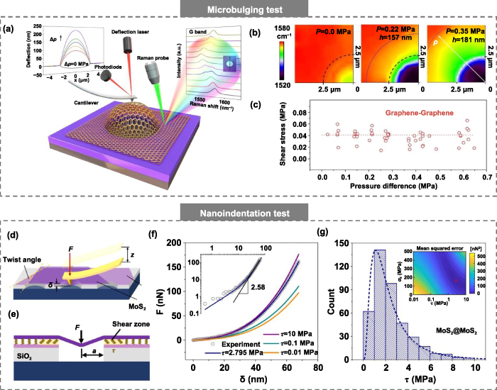
Figure 14. Representative studies of the interfacial shear properties leveraging out-of-plane deformation of 2D materials. (a) Schematic diagram of a bilayer graphene bulging device paired with Raman spectroscopy. (b) Raman contour maps of the G-band frequency revealed the strain distribution in bilayer graphene. (c) Measured shear stresses for interlayer interfaces between graphene. Reprinted figure with permission from [45], Copyright (2017) by the American Physical Society. (d) Schematic diagram of AFM deflection tests on twisted bilayer MoS2. (e) Schematic of the AFM deflection process on a 2D membrane that considers an interfacial shear zone between the tested membrane and the substrate. (f) Comparison between one typical experimental curve and fitted curves based on the theoretical model. (g) Distribution of fitted shear stresses that satisfies a logarithmic normal distribution. The inset shows a contour map of the nonlinear fitting error to obtain the closest shear stress of this sample. Reproduced from [313]. CC BY 4.0.
Download figure:
Standard image High-resolution imageSimilarly, the shearing boundary model was also applied to twisted bilayer MoS2 in an AFM deflection study [313], as illustrated in figure 14(d). By incorporating the shear stress in the mechanics model (figure 14(e)), modifications to the nonlinear fitting bring better alignment between theoretical predictions and experimental data (figure 14(f)). Consequently, the statistical average interlayer shear stress is given as 2.51 MPa as summarized in figure 14(g), which is much lower than that between MoS2 monolayer and SiO2 substrate (11.09 MPa). Moreover, the interlayer shear stress exhibits an independence of the twist angle. This result is explained by the fact that the overall interlayer vdW interaction is the sum of long-range intermolecular forces, which homogeneously spread over the interfaces of 2D materials.
5.2.3. Raman-tensile test for interfacial characterization.
Apparent interlayer sliding has also been observed between two randomly stacked graphene layers on polymer substrates, subjected to four-point bending [314] (figure 15(a)). The evolution of Raman spectra was recorded with increasing load, where the Raman 2D-band split into two subpeaks that exhibit distinct Raman shift rates, suggesting different stress transfer efficiency at graphene–graphene and graphene-polymer interfaces. On the basis of shear-lag analysis, the interlayer shear stress can be estimated based on Raman mapping of the strain distribution along the length of the graphene flake, in the range of ∼0.04–0.13 MPa and ∼0.04–0.16 MPa for exfoliated and CVD samples respectively (figures 15(b)–(d)).

Figure 15. Representative studies of the interfacial shear properties via Raman-based tensile tests. (a) Four-point-bending setup for uniaxial tension of bilayer graphene with random incommensurate stacking. (b) Schematic of the stress transfer mechanism from the polymer substrate to the bottom layer and from the bottom layer to the top layer. (c) The distribution profile of Raman 2D-band frequency across the length of top layer graphene of the folded bilayer. (d) Interface and interlayer shear stress for graphene/polymer and graphene/graphene configurations at various strains. Reproduced from [314]. CC BY 4.0. (e) Schematic diagram of the in-plane tensile setup. (f) Schematic diagram of in situ Raman and PL spectroscopy/micro-tensile testing analysis of graphene/MoS2/PET substrates, which give rise to strain contour maps (left) of each layer in the heterostructure. (g) The evolution of the interlayer strain as a function of PET strain during the loading process. (h) Interfacial shear stress (ISS) distributions of two interfaces along with a centerline position of graphene/MoS2 on PET. Reprinted from [316], Copyright (2022), with permission from Elsevier.
Download figure:
Standard image High-resolution imageFollowing the same analysis, Dou et al [315] further explored the effect of the stacking mode on the interlayer shear properties of bilayer polycrystalline graphene. An interlayer shear strength of 0.084 MPa was revealed, which is consistent with existing works. Note that, for transferred bilayer graphene with unequal flake sizes, stress concentrations occurred around the boundary of the smaller layer graphene flakes due to the abrupt change of material thickness. When the upper layer is larger than the substrate-facing layer of graphene, the stress concentration caused by this stacking arrangement is larger, reaching peak values in the range of 0.7–1.0 GPa.
In contrast to graphene, photoluminescence (PL) spectroscopy was found to be more effective for strain characterization of TMDs (e.g. MoS2), because of its sufficiently large variation in Raman peak shift per unit strain as well as small dispersion of the PL peak positions. Combining Raman and PL spectroscopy, the local strain fields of graphene and MoS2 (substrate-facing) flakes were monitored during the loading process (figures 15(e)–(f) [316]). The deformation evolution and transfer mechanism between two types of interfaces of Graphene/MoS2 and MoS2/polyethylene terephthalate (PET) in the heterostructure were further analyzed based on the Raman and PL responses, showing that the upper graphene entered the sliding regime earlier than the PET-facing MoS2 (figure 15(g)). The interlayer shear properties of such graphene/MoS2 heterostructures were quantified based on shear-lag analysis as shown in figure 15(h), giving rise to a shear strength of 0.19 MPa, which is lower than that of MoS2/PET (0.34 MPa).
5.3. Interfacial properties between 2D materials and 3D substrates
5.3.1. Shear-lag analysis.
2D materials feature atomically smooth surfaces and weak out-of-plane vdW interactions, leading to a low interfacial shear strength [317, 318]. Upon increasing the applied load, interfacial shear stress will rise to a critical level (e.g. the interfacial shear strength) upon which slippage begins. In contrast to macroscale interfacial shearing, at the nanoscale friction and adhesion can occur in absence of an applied normal pressure [319]. Interestingly, a steady sliding behavior has been captured at the interface beyond the elastic stage, where the interfacial shear stress remains the same as the displacement increases. This can be ascribed to the repetitive breaking-and-reforming characteristic of vdW interactions, as reflected by stick–slip behavior in the interfacial energy or shear traction versus displacement curves [320].
As such, shear interactions between 2D materials and polymer substrates have been examined by deforming flexible substrates to induce relative sliding. For example, monolayer graphene on a stretchable substrate can be strained by stretching the substrate, which transfers an axial stress into the graphene through interfacial shear tractions. By measuring the strain distributions in the graphene, e.g. by Raman spectroscopy, the interfacial shear traction between graphene and the substrate can be deduced from a shear-lag analysis [321] (figure 16(a) and (b)). In particular, Jiang et al assumed a linear relation between the interfacial shear traction and the relative sliding displacement followed by a constant traction as the interfacial shear strength in their analysis of microscale monolayer graphene flakes on a stretchable PET substrate [322]. They obtained values of the graphene/PET interfacial shear strength between 0.46 and 0.69 MPa, which are comparable to those for other polymer-based systems [12, 322, 323].
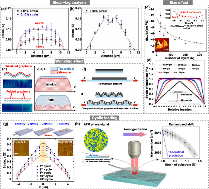
Figure 16. Representative studies for the interfacial properties between 2D materials and 3D substrates. Distribution of strain in the hBN nanosheet in the direction of the tensile axis at (a) 0.05%, 0.10% strain and (b) 0.30% strain. (c) Raman G-band shift rate of hBN nanosheets as a function of number of layers. Reproduced from [329]. © The Author(s). Published by IOP Publishing Ltd. CC BY 4.0. (d) Distributions of strain of graphene with eight different lengths after failure of the interface. Reprinted with permission from [325]. Copyright (2016) American Chemical Society. (e) Schematic of wrinkled and folded graphene as well as their strain distributions. Reproduced from [330]. © IOP Publishing Ltd. All rights reserved. (f) Schematic of the stress transfer mechanism in wrinkled multilayer graphene on a polymer substrate. Reprinted with permission from [332]. Copyright (2017) American Chemical Society. (g) Strain distribution in the direction of the stretching axis of a graphene sheet at a strain level of 0.7% after multiple loading/unloading cycles. The insets show the corresponding AFM topography images. Reprinted from [331], Copyright (2017), with permission from Elsevier. (h) A schematic showing in situ Raman spectroscopy during uniaxial tensile testing, presenting a nonlinear strain dependence in the Raman shift due to the nonuniform local conformity of the graphene/substrate interface, as reflected in the AFM phase signal. Reprinted with permission from [333]. Copyright (2021) American Chemical Society.
Download figure:
Standard image High-resolution imageInterfacial stress transfer has also been evaluated for hBN/PMMA and MXene/PMMA systems using shear lag theory [324]. Specifically, the interfacial shear strength between MXenes and PMMA was evaluated to be of the order of 3–4 MPa, similar to that of graphene, indicating that the stress transfer at the MXene/polymer interface occurs through vdW interactions. In contrast, the interfacial shear stress between the hBN and the PMMA substrate is of the order of 10 MPa, a factor of around 4 higher than that for a monolayer graphene (∼2.3 MPa).
5.3.2. Size effect.
Experiments by Xu et al [325] found that the interfacial shear strength between graphene and the PET substrate exhibits a lateral size-dependency that decreases by two orders of magnitude when the graphene sample length is increased from ∼20 µm to 10 mm, as shown in figure 16(c). In particular, the macroscopic CVD graphene sheet (length of ∼1 cm) has been demonstrated to show a much lower interfacial shear strength of 0.004 MPa. The effect of multiscale surface roughness could be the key to understanding such a dependence on lateral dimension. Namely, a shorter length of graphene facilitates a better conformation and hence stronger bonding at the interface. As a result, the stress transfer and interfacial property of graphene exhibit a size dependence, as characterized by the transfer length.
A size effect was also observed in the thickness direction, which may be attributed to interlayer sliding behavior in 2D materials. Typically, the Raman G-band or 2D band shift is utilized to estimate strain conditions of 2D materials, where tensile strain induces phonon softening (red shift), while compression induces phonon hardening (blue shift [326, 327]). Consequently, the Raman shift rate reflects the load transfer efficiency at the interfaces, which can be simply defined by the ratio of the Raman shift rate of multilayers to monolayers. Previous studies by Gong et al [328] reported an insufficient load transfer between graphene layers when exposed to a uniaxial stretching on SU-8 epoxy resin. While the Raman shift rate for monolayer and bilayer graphene is approximated to be 52 cm−1/%, it reduces to 8 cm−1/% for multilayers. Compared to graphene, the efficiency of internal stress transfer between the neighboring hBN [329] layers was found to be of the order of 99% compared to around 70% for multilayer graphene, as a result of the stronger electrostatic bonding between the hBN layers (figure 16(d)). Similar thickness-independent interfacial mechanical measurements were also demonstrated for MXenes [324], indicating a better interlayer stress transfer between Ti3C2Tx layers, which is facilitated by the cohesive functional groups in the interlayer gallery.
5.3.3. Wrinkling effect.
As a 2D monolayer with limited bending rigidity, graphene is vulnerable to out-of-plane folding and buckling (e.g. wrinkling). The presence of wrinkles greatly influences the efficiency of graphene as a reinforcement in nanocomposites, where delamination at wrinkles can adversely affect the stress transfer process (figure 16(e)) [330]. For instance, a previous study found that the interfacial sliding-induced strain mismatches between graphene and polymer substrates result in compressive stresses that buckle and delaminate graphene during unloading from 1% strain. This buckling impairs the contact and adhesion at graphene/polymer interface, but also separates the entire flake into patches with lateral dimensions even below the critical length. As the critical length is defined as the minimum length required to completely load the graphene, the sectionalized small-sized graphene domains are detrimental to the overall interfacial load transfer [331].
Conversely, if the wrinkled graphene conforms to the polymer substrate, the interfacial shear strength can be maintained or even improved. This is explained by the rough surface of graphene that leads to enhanced nanofiller/matrix adhesion and interlocking at the interface as shown in figure 16(f). In addition, the wrinkled network was found to further improve the interlayer friction in few-layer graphene and exhibit a thickness independence of the interfacial stress transfer efficiency [332]. The maximum shear stress can reach as high as ∼0.75 MPa for a trilayer wrinkled graphene/polymer interface, much higher than values obtained from flat, simply supported graphene/polymer systems at similar strain levels. Apparently, creating wrinkle patterns in graphene provides a new avenue to enhance the load bearing capability of graphene fillers. Moreover, it outperforms chemical surface treatments as mechanical integrity of carbon nanofillers is maintained without the introduction of structural defects.
5.3.4. Cyclic loading.
Nanocomposite materials or 2D material-based flexible devices are frequently subjected to cyclic loads for both scientific and industrial applications, where mechanical degradation and damage have been observed at weak vdW interfaces. For instance, upon the cyclic loading, graphene undergoes slippage on polymer substrates during the loading and then compression during unloading. Wang et al [331] performed Raman mapping to monitor the interfacial stress transfer process and revealed the weakening of graphene/PMMA interface under cyclic loading. An in-plane uniaxial strain level up to 0.7% was applied to the graphene/PMMA composite system to ensure interfacial sliding at the center of the graphene sheet, and hence a triangular-shaped strain distribution was generated. During multiple loading/unloading cycles, the slope of strain gradient that determined the interfacial shear strength decreased and confirmed the weakening of stress transfer (figure 16(g)). The degradation mechanism was found to be caused by buckling, which formed from the in-plane compression during the unloading stage, as captured by AFM topography imaging. Intuitively, increasing loading cycles causes larger buckling amplitudes and increased roughness. Interestingly, macroscopic CVD graphene, with wrinkles formed during the growth or transfer process, exhibits a distinct interfacial mechanical response to cyclic loading, which stands in contrast to mechanically exfoliated graphene. A recent experimental study by Xu et al [333] noted that CVD grown graphene/PET samples displayed an enhanced interface adhesion when treated with cyclic stretching with incremental strain amplitude. However, the as-transferred sample showed an abnormally low and nonlinear Raman shift rate, due to the nanometer-scale inhomogeneity of strain caused by the non-uniform interface conformity (figure 16(h)). The cyclic loading induced the slip of graphene against the substrate and re-established the interfacial contact quality, where some of the folds are stretched to conform to the substrate, increasing the interfacial contact area as well. As a result, quantitatively, the interfacial shear strength between graphene and PET was reported to increase from 0.152 MPa to 0.305 MPa after cyclic loading treatment at a maximum strain amplitude of 1.0% [334].
In addition to the above-mentioned Raman-based technique, tensile testing induced periodic cracks can also enable the evaluation of interfacial shear strength. For example, uniaxial stretching of polycrystalline graphene on a copper foil under SEM revealed regularly spaced channel cracking in the graphene [215]. The density of the channel cracks increased with increasing applied strain until a minimum spacing was obtained. The crack patterns were analyzed using a classical shear lag model to extract the shear strength according to the minimum crack spacing. The obtained value of 0.49 MPa is similar to those between graphene and polymers. Similarly, a necking-assisted fragmentation method has been recently proposed to controllably fabricate ordered graphene ribbons [217]. Based on the known fracture toughness of graphene (16.5 J m−2) and the measurement of ribbon widths, the interfacial shear strength was deduced to be 3.1 MPa. Sharing a similar mechanism, the periodic wrinkles generated during uniaxial compression can be alternatively exploited to quantify the interfacial shear properties [335]. By replacing the fracture toughness and ribbon width with interface adhesion and wrinkle period, maximum interfacial shear strengths on PDMS of 3.8 ± 0.8 MPa and 7.7 ± 2.5 MPa are measured for graphene and MoS2, respectively.
5.3.5. Atomistic simulations of interfacial shear properties for 2D material-based nanocomposites.
The parallel computing capabilities of atomistic simulations offer attractive opportunities to rapidly screen a variety of interfaces in 2D systems. This computation-led materials discovery workflow is of particular importance for 2D material-based nanocomposites, where a large design space of material pairings exists. While the in-plane properties of 2D materials are notably impressive, load transfer and cohesion requirements of composites necessitate consideration of interplanar bonding behavior. Within this context, the related systems of graphene and GO offer an interesting benchmark. Graphene, which possesses the highest in-plane stiffness and strength, exhibits notably weak interfacial shear properties. The poor interfacial cohesion of graphene can be overcome through surface chemistry modification, with GO being a well-known product of this functionalization. Yet, while the introduction of functional groups can bring improvements to the interfacial shear properties of graphene, it ironically leads to a decrease in the in-plane properties. For instance, GO possesses a range of moduli and strengths, which decrease monotonically with the level of oxidation. Using the DFTB method, Wei et al [5] report elastic moduli and strengths in the range of 218–542 GPa and 15–34 GPa, respectively for GO samples with a 4:1 epoxide:hydroxyl functionalization ratio at various oxidization levels. As demonstrated by this and related studies, the selection of 2D materials as constituents for nanocomposites therefore requires careful balancing of tradeoffs between the in-plane and out-of-plane properties. In this regard, tuning of interfacial behavior by functionalization of 2D monolayers becomes of primary interest. This prospect naturally opens a wide parametric design space for 2D materials. In lieu of exhaustive experimentation, computational approaches such as atomistic simulations have been leveraged by the community to map the functionalization space of many 2D materials, with GO being the most studied.
The earliest computational work on tuning the interlayer behavior of GO is found in a pair of studies from Wei et al [5] and Compton et al [336]. Here, the focus on the role of hydrogen bond networks formed between functional groups and intercalated water molecules in GO may be used to tune the interfacial mechanical response. More recently, Soler-Crespo et al [337] used MD to measure the interfacial shear tractions between GO bilayers with varying amounts of intercalated water. A key interpretation from this study is that environmental conditions (e.g. relative humidity) play a mediating role in defining interfacial shear properties that rivals the importance of GO surface chemistry and functionalization in interlayer cohesion. In addition to interfacial shear interactions between GO layers, the scale-up to GO-based nanocomposites require consideration of GO-matrix interactions. Espinosa and co-workers have performed MD studies of the interfacial shear properties of polyvinyl alcohol (PVA) and polyethylene glycol chains intercalated between GO layers [338]. Here, the GO-PVA system was found to offer the highest interfacial shear strength due to the donor-acceptor character of the hydrogen bonds in this polymer. Their report highlights the importance of the character of hydrogen bonds (e.g. donor-acceptor) as a pathway to screen polymers for 2D materials-based composite design. In addition to GO-based studies, computational reports of other 2D nanocomposites have begun to emerge, with the MXene-polymer system receiving some recent attention [339, 340].
6. Adhesion
The adhesive properties of 2D materials are critical to the assembly and scale-up of 2D material-based structures/devices [341–343]. A diverse set of methodologies have been developed to investigate the interactions between 2D materials and various mating surfaces (e.g. their growth substrates [344–348], homo-/hetero-interfaces [346, 349–353], and common device substrates [12, 354]). The adhesion energy is the most common metric used to evaluate the adhesive interactions between a 2D material and a surface, which defines the energy required per unit area to separate a 2D material interface. Current experimental methods to quantify adhesion energy of 2D materials primarily include indentation (e.g. approach a 2D material with a probe and separate the interface [350, 351, 355]), blister testing (e.g. bulging a 2D material on a substrate with a hole to create a separation at the interface [40]), double cantilever beam (e.g. DCB, peeling a 2D material from a substrate by mode I fracture [356]), scratch testing (e.g. scratch a 2D material on a surface until wear happens [350, 356, 357]), and polymer-based delamination test (e.g. release a pre-stretched 2D material/polymer laminate to cause compression induced buckling/wrinkling at the interface [317, 358–360]). During the revision process of this review article, a new in-situ SEM-based method was published, which enables simultaneous measurement of both modulus and adhesive properties by pull-to-peel of a suspended 2D material [361]. While variations of each measurement technology exist, the fundamental working concepts are similar. A recent review detailed the evolution of these technologies and analyzed the benefits and drawbacks of different technologies [359]. In this section, we will briefly discuss some key developments in methods for adhesion measurements and will focus on providing a comparison of the adhesive properties of 2D material systems.
6.1. Methodologies
6.1.1. Indentation-based methods.
Indentation tests by a micro-indenter [351, 362] or AFM [350, 351, 355] have been applied to investigate the adhesion energy of 2D interfaces. The working principle for either technique is similar and entails extracting force–displacement (F–d) curves during contact-retract process between the indenter and a substrate. The obtained F–d curves are leveraged to calculate the adhesion energy either by fitting the curves into a contact mechanics model [362] or through integration of the traction separation data [351]. The indenter and substate can both be coated with 2D materials such that the adhesive properties between 2D interfaces can be investigated [351, 363, 364]. The primary benefit of micro indenter-based techniques is to be able to measure large adhesion, which is enabled by the wide force ranges of the instrument used, while the AFM-based nanoindentation offers high measurement precision.
A very recent work in adhesion measurement among 2D material interfaces adopts an AFM-based nanoindentation method using customized probes with a well-defined geometry, such that the contact area between the indenter and a substrate can be accurately measured (figure 17(a) [351]). Prefabricated 2D crystal mesas can also be attached to the indenter tip to allow measurement of adhesion between two 2D interfaces. Measurement by this method is straightforward for analysis of adhesion energy, where it is calculated by simply integrating the obtained traction separation curves, followed by normalization over the contact area between the interfaces. Applying this method to graphene, MoS2 and hBN as benchmark 2D material systems, Rokni and Lu [351] measured the adhesion energies between these 2D materials and a SiO2 substrate, as well as their homo- and hetero-interfaces.
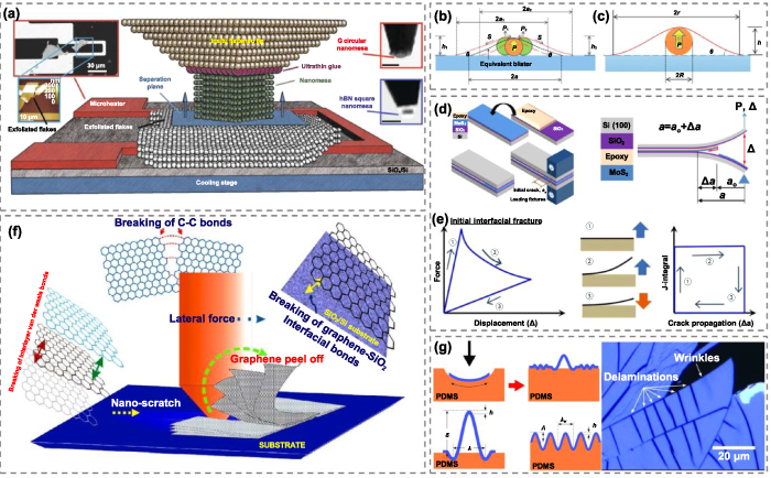
Figure 17. Schematics of experimental setups for the measurement of adhesive properties of 2D materials. (a) Indentation-based methods; Reprinted by permission from Springer Nature Customer Service Centre GmbH: Springer Nature, Nat. Commun [351]. (c) 2020. (b) and (c) Blister testing; [365] John Wiley & Sons; (d) and (e) The double cantilever beam (DCB) method; Reprinted by permission from Springer Nature Customer Service Centre GmbH: Springer Nature, Sci. Rep. [356]. (c) 2017. (f) Scratch testing; Reprinted from [357], Copyright (2013), with permission from Elsevier. (g) Elastomer-based instability test. [344] John Wiley & Sons.
Download figure:
Standard image High-resolution image6.1.2. Blister testing.
Measurement of adhesive properties of 2D materials by blister testing is another common approach. However, so far, the blister tests are limited to measuring adhesion between 2D materials and a substrate but not between homo- and hetero-interfaces in 2D material stacks. The working principle is to create a 2D material blister by generating a pressure difference normal to the surface of a suspended 2D membrane. Various methods to generate a pressure difference have been developed (i.e. hydrogen irradiation, Ne ion sputter, etc) and reviews on this topic are also available [62, 366]. The adhesion energy between the 2D material and a substrate can subsequently be calculated based on the geometry of the blister, the pressure difference, and/or other properties of the system [40].
More recently, a facile testing method using nanoparticles to create blisters has been developed by Zong et al [367]. In this technique, nanoparticles are spread on a substrate and then covered by the deposition of a 2D material, which creates a network of supported blisters (figure 17(b) [365]). The adhesion energy can then be calculated from the measurement of the geometry of the supported blister. A notable advancement of this technique is presented by Gao et al [365], which relaxes the requirement for isolated spherical particle supports [367]. Using Gao's method, the adhesion energy can be calculated from single spherical or dual elliptical blister geometries (figure 17(c)) which substantially improves the practical implementation of the method. When a single spherical particle is covered with a 2D material flake (figure 17(c)), the adhesion energy (Γ) at the film substrate interface can be expressed as:
where E is the in-plane elastic modulus of the 2D material, t is the thickness of the 2D material, h is the blister height, and r is the blister radius. In the case where two particles are trapped under a 2D material flake (figure 17(b)), the adhesion energy (Γ) at the interface can be calculated based on equation (12) by replacing blister radius (r) with debonding radius (a). The assumptions here are (1) the two particles are identical and have the same debonding radius (a1 = a2) and blister height (h1 = h2); (2) both blisters are axisymmetric and tangent to each other; (3) angles subtended by the 2D material, θi (i = 1, 2), are the same for both particles. Adhesion energies for mono, few-layer and multilayer graphene on SiO2 substrates were measured via this method. In addition, there is another recent stream of similar research that measures the adhesion of 2D materials and substrates by examining the blisters formed spontaneously during transfer of 2D materials, which can also be leveraged as a new tool for the characterizations of interfacial adhesion and the bending stiffness of 2D materials [341, 346, 368].
6.1.3. DCB method.
The DCB method is another common technique for measurement of adhesive properties between 2D materials and substrates. The DCB method exhibits many parallels to peel-off type delamination experiments, with the 2D material/substrate interface positioned on one of the cantilevers. The exposed 2D material surface is then rigidly glued to the opposing cantilever with an intentional overhang. The cantilevers are then separated to propagate a crack from the overhang and the tensile loads are recorded to determine the work of separation, which yields the adhesion energy (figure 17(d) [356]). Based on linear fracture mechanics and beam theory, the crack length (a) can be calculated by equation (13):
where P is the applied force, E is the in-plane elastic modulus of the substrate, b is the width of the substrate, t is the thickness of the substrate, Δ is the displacement. As shown in figure 17(e), the three stages of the tensile test are: the ramp-up of load to initiate crack propagation, separation of the glued interfaces, and the release of the load. After the crack lengths are calculated at different load levels, the adhesion energy can be determined from the energy release rate (G) at the interface,
Leveraging this method, Na et al [356] reported the adhesion interaction between MoS2 and silicon oxide.
6.1.4. Scratch test.
Measuring adhesive properties at an interface using scratch tests has a long history and has been applied to a diverse set of systems such as thin films [369] and one-dimensional materials [350]. Das et al [357] applied the technology to measure the adhesion energy between a 2D material and metallic substrates (e.g. graphene/Cu and graphene/Ni) (figure 17(f)). The working concept is simple: applying a lateral force to make a scratch on the surface of a 2D material on a substrate to cause debonding or 'peel-off' of the 2D material. The experimentally obtained lateral force versus lateral displacement can be used to extract adhesion energy at the interface by integrating the area under the curve. Using this method, the adhesion energy at the graphene/Ni interface was measured to be 72.7 J m−2, and that of the graphene/Cu 12.75 J m−2.
6.1.5. Elastomer-based instability test.
The transfer of 2D material flakes onto an elastomer substrate is another method to quantify the adhesive properties of 2D materials. Here, the large elastic mismatch between the stiff 2D materials and a compliant elastomer is leveraged to create an interfacial instability, which delivers the adhesion energy. As presented in figure 17(g), both buckling and wrinkling can happen after the release of pressure. The adhesion energy can be calculated by using the following equation:
where Γ is the adhesion energy, δ is the delamination height, λ is the delamination width, h is the film thickness, E is the in-plane elastic modulus, and  is the Poisson's ratio of the film. It is apparent that Γ is very sensitive to h, δ, and λ, which makes accurate measurement of these parameters important to minimize uncertainty. For delamination height and width, AFM topography images are accurate enough to extract their values with sufficient precision (∼100 nm–µm). However, the film thickness is much more challenging to measure by AFM. That is, the large elastic stiffness mismatch between 2D materials and elastomers can result in an artificial increase in the AFM step height. To circumvent this issue, a buckling mechanics model can be applied to the wrinkles formed during testing to indirectly extract the thickness:
respectively, where  and
and  are the amplitude and period at the onset of wrinkling at a critical strain point
  . In these equations, ξ = 5pre(1 + pre)/32, while
  and
and  are the plane-strain moduli of the 2D material and the PDMS, respectively. The plane-strain modulus is defined as
  = E/(1 − v2). Therefore, h and pre can act as two fitting parameters for equations (16) and (17) when the wrinkle amplitude and wavelength are known.
6.2. Comparison of experimentally measured adhesion energies of 2D interfaces
Graphene, MoS2 and MXenes are chosen as three representative 2D material types for comparison here because their adhesive properties are the most represented in the literature. Experimentally measured adhesion energies between these three materials and various substrates are summarized in table 4 and figures 18–20. These data are not intended to represent an exhaustive list of measurements, but rather impress upon the reader the wide scatter of data available in the literature.
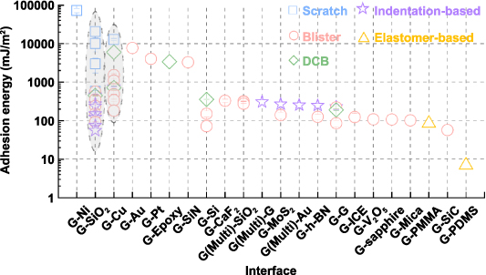
Figure 18. Adhesion energies at interfaces between graphene and various surfaces experimentally measured by different methods.
Download figure:
Standard image High-resolution image
Figure 19. Adhesion energies at interfaces between MoS2 and various surfaces experimentally measured by different methods.
Download figure:
Standard image High-resolution image
Figure 20. Adhesion energies at interfaces between MXene and various surfaces experimentally measured by indentation methods.
Download figure:
Standard image High-resolution imageTable 4. The adhesion between 2D materials and substrates included in this review.
| Interface | Layer number | Adhesion energy (mJ m−2) | Measurement technique | Reference |
|---|---|---|---|---|
| Graphene-SiO2 | Monolayer | 453 ± 6 | Blister | [365] |
| Graphene-SiO2 | 3–5 layer | 317 ± 3 | Blister | [365] |
| Graphene-SiO2 | 10–15 layer | 276 ± 2 | Blister | [365] |
| Graphene-SiO2 | Monolayer | 460 ± 20 | Indentation | [355] |
| Graphene-SiO2 | Monolayer | 567 | Blister | [375] |
| Graphene-SiO2 | Monolayer | 580 ± 20 | Indentation | [349] |
| Graphene-SiO2 | Monolayer | 357 ± 16 | DCB | [376] |
| Graphene-SiO2 | 2–5 layer | 310 ± 30 | Blister | [40] |
| Graphene-SiO2 | Monolayer | 450 ± 20 | Blister | [40] |
| Graphene-SiO2 | Monolayer | 270 ± 20 | Indentation | [350] |
| Graphene-SiO2 | Monolayer | 239 ± 54 | Indentation | [351] |
| Graphene-SiO2 | Monolayer | 151 ± 28 (for E = 0.5 TPa) | Blister | [367] |
| Graphene-SiO2 | Monolayer | 240 ± 50 | Blister | [377] |
| Graphene-SiO2 | Monolayer | 93 ± 1 | Blister | [346] |
| Graphene-SiO2 | Monolayer | 2978 ± 1240 (as transferred) | Scratch | [369] |
| Graphene-SiO2 | Monolayer | 10 090 ± 4050 (after rapid thermal annealing) | Scratch | [369] |
| Graphene-SiO2 | Monolayer | 20 640 ± 7040 (after vacuum annealing) | Scratch | [369] |
| Graphene-SiO2 | Monolayer | 74.4 ± 2.7 (for approach, DMT) | Indentation | [362] |
| Graphene-SiO2 | Monolayer | 55.5 (for approach, FEM) | Indentation | [362] |
| Graphene-SiO2 | Monolayer | 121 ± 10.3 (for withdrawal, DMT) | Indentation | [362] |
| Graphene-SiO2 | Monolayer | 149 (for withdrawal, FEM) | Indentation | [362] |
| Graphene-Cu | Monolayer | 750 ± 20 | Indentation | [355] |
| Graphene-Cu | Monolayer | 740 ± 130 (acetic acid for 4 h) | Blister | [370] |
| Graphene-Cu | Monolayer | 1100 ± 160 (acetic acid for 24 h) | Blister | [370] |
| Graphene-Cu | Monolayer | 1530 ± 110 (acetic acid for 48 h) | Blister | [370] |
| Graphene-Cu | Monolayer | 341 ± 24 (simple plate model) | Blister | [371] |
| Graphene-Cu | Monolayer | 484 ± 7 (modified plate model) | Blister | [371] |
| Graphene-Cu | Monolayer | 182 (at a mode-mix of −45°) | Blister | [372] |
| Graphene-Cu | Monolayer | 720 ± 70 | DCB | [373] |
| Graphene-Cu | Monolayer | 6000 | DCB | [374] |
| Graphene-Cu | Monolayer | 12 800 ± 1000 | Scratch | [357] |
| Graphene-Au | Monolayer | 7687 | Blister | [375] |
| Graphene-Au | Multilayer | 255 ± 35 | Indentation | [350] |
| Graphene-Ni | Monolayer | 72 700 ± 10 000 | Scratch | [357] |
| Graphene-SiN | Monolayer | 3282 | Blister | [375] |
| Graphene-Pt | Monolayer | 4021 | Blister | [375] |
| Graphene-Graphene | Monolayer | 86 ± 16 | Blister | [346] |
| Graphene-Graphene | Multilayer | 307 ± 40 | Indentation | [350] |
| Graphene-Graphene | Monolayer | 230 ± 35 | Indentation | [351] |
| Graphene-Graphene | monolayer | 190 ± 10 | DCB | [352] |
| Graphene-Graphene | Monolayer | 221 ± 11 | Blister | [353] |
| Graphene-MoS2 | Monolayer | 140 ± 26 | Blister | [346] |
| Graphene-MoS2 | Monolayer | 269 ± 38 | Indentation | [351] |
| Graphene-hBN | Monolayer | 126 ± 20 | Blister | [346] |
| Graphene-hBN | Monolayer | 248 ± 35 | Indentation | [351] |
| Graphene-Ice | Monolayer | 124 ± 30 | Blister | [346] |
| Graphene-CaF2 | Monolayer | 330 ± 30 | Blister | [347] |
| Graphene-V2O5 | Monolayer | ⩽108 | Blister | [348] |
| Graphene-Mica | Monolayer | ⩽102 | Blister | [381] |
| Graphene-Si | Monolayer | ⩽72 | Blister | [345] |
| Graphene-Si | Monolayer | 151 ± 28 | Blister | [367] |
| Graphene-Si | Monolayer | 357 ± 16 | DCB | [376] |
| Graphene-Epoxy | Monolayer | 3400 | DCB | [374] |
| Graphene-PMMA | Monolayer | 84.4 | Buckling | [12] |
| Graphene-SiC | Monolayer | ⩽57 | Blister | [382] |
| Graphene-sapphire | Monolayer | ⩽107 | Blister | [383] |
| Graphene-PDMS | Multilayer | 7 | Buckling | [354] |
| MoS2-SiO2 | Monolayer | 82 ± 1 | Blister | [346] |
| MoS2-SiO2 | Monolayer | 482 | Blister | [375] |
| MoS2-SiO2 | Multilayer | 220 ± 35 | Blister | [42] |
| MoS2-SiO2 | Multilayer | 2200 ± 100 | DCB | [356] |
| MoS2-SiO2 | Multilayer | 170 ± 30 | Buckling | [384] |
| MoS2-SiO2 | Monolayer | 189 ± 27 | Indentation | [351] |
| MoS2-SiN | Multilayer | 429 | Blister | [375] |
| MoS2-Si3N4 | Multilayer | 252 ± 41 | Buckling | [384] |
| MoS2-PDMS | Multilayer | 18 ± 2 | Buckling | [344] |
| MoS2-Au | Multilayer | 1207 | Blister | [375] |
| MoS2-Pt | Multilayer | 691 | Blister | [375] |
| MoS2-Al2O3 | Multilayer | 101 ± 15 | Blister | [346] |
| MoS2-MoS2 | Monolayer | 174 ± 18 | Blister | [346] |
| MoS2-MoS2 | Monolayer | 384 ± 42 | Indentation | [351] |
| MoS2-hBN | Monolayer | 136 ± 11 | Blister | [346] |
| MoS2-hBN | Monolayer | 262 ± 25 | Indentation | [351] |
| hBN-hBN | Monolayer | 129 ± 4 | Blister | [346] |
| hBN-hBN | Monolayer | 259 ± 32 | Indentation | [351] |
| hBN-SiO2 | Monolayer | 208 ± 47 | Indentation | [351] |
| Ti2CTx -SiO2 | Monolayer | 390 ± 20 | Indentation | [349] |
| Ti3C2Tx -SiO2 | Monolayer | 880 ± 20 | Indentation | [349] |
| Graphene-Ti2CTx | Monolayer | 590 ± 30 | Indentation | [349] |
| Ti2CTx -Ti2CTx | Monolayer | 580 ± 20 | Indentation | [349] |
| MoSe2-Ti2CTx | Monolayer | 270 ± 20 | Indentation | [349] |
| Ti2CTx -Ti3C2Tx | Monolayer | 930 ± 30 | Indentation | [349] |
| Graphene-Ti3C2Tx | Monolayer | 790 ± 30 | Indentation | [349] |
| Ti3C2Tx -Ti2CTx | Monolayer | 880 ± 30 | Indentation | [349] |
| Ti3C2Tx -Ti3C2Tx | Monolayer | 1220 ± 20 | Indentation | [349] |
| MoSe2-Ti3C2Tx | Monolayer | 370 ± 30 | Indentation | [349] |
| MoSe2-SiO2 | Monolayer | 270 ± 30 | Indentation | [349] |
In figure 18, the adhesion energies for graphene-based interfaces are plotted. A general insight from the plot is that even though vdW interactions are considered the most dominant force at these interfaces, the reported adhesion energies between graphene and surfaces span several orders of magnitude. Also, there are significantly more studies for certain interfaces than others. For example, many adhesion experiments have been performed between graphene-Cu and graphene-SiO2 interfaces, given the history of Cu as a common growth substrate for CVD graphene, and SiO2 is used most extensively as a flat substrate for 2D materials studies [40, 367]. While the measurement scatter is reduced between graphene and other substrates [40, 346, 350, 351, 355, 357, 362, 365, 367, 369–377], the overall agreement in values is still poor. Furthermore, some elements of statistical scatter may be masked by the comparatively lower number of experiments in these systems. Similar observations can be made for the adhesion energy measurements of MoS2-based interfaces (figure 19). While MoS2–SiO2 interface is a more commonly studied interface in the literature, unfortunately the measured values are also scattered across a couple of orders of magnitude. One reading of the data would indicate that adhesion energies between graphene or MoS2 and metals are generally the highest compared to other substrates, which has also been demonstrated in computational studies [362]. However, current available experimental results cannot fully resolve the inconsistencies in the literature due to the lack of testing standards and variations in methodologies among studies. The literature on the adhesion of MXene interfaces is still emerging and not many adhesion studies at MXene interfaces are found (figure 19 [349, 363]), which makes it difficult to draw any conclusion, given the high dependence of these studies on experimental conditions and protocols.
The inherent complexity of adhesion energy measurements at 2D interfaces presents a challenge to finding the source of scatter in the literature. However, the measurement techniques/analysis applied, the qualities/types of samples prepared and the environmental conditions of the experiment are all significant parameters. Indeed, sufficient data exists to suggest that the source of scatter stems in part from different practices across labs. Taking the graphene-SiO2 interface as an example, it is apparent that the AFM-based nanoindentation techniques can introduce several uncertainties in the adhesion measurement. The humidity level can affect the interactions between the AFM tip and a substrate [378] (e.g. capillary effect [351], double ice layer on 2D material [378], etc); adhesion measurement can also be affected by whether 2D materials were tested on a substrate or in suspension [358]; and even small pre-sliding on the 2D material surface before pull-off can result in differences in measurements [379]. Additional complicating parameters include the quality of sample [355, 375] (CVD versus single crystal), roughness at the interfaces [346, 373], contaminants [346], instrumental errors, and the size of contacts [380], among others.
Thus, it is very difficult to make equitable comparisons among different studies to draw convincing conclusions on the reliability of datasets and precise measurement values. The challenges associated with the comparison of measurements in 2D materials represent perhaps a limiting extreme of this widely acknowledged issue within the nanoscience community. Moreover, a standard or a consensus in the field is imperative to translate nanoscale discoveries into practical applications. For example, sufficient precision in measurements of adhesion energies is a requirement for the development of large-scale and high-throughput transfer printing technologies, which is a milestone in the transfer of lab-scale 2D sciences to 2D materials-based devices in the marketplace. Based on the interpretations gathered for this review, we would like to underscore the importance of rigorous measurements for the following parameters related to adhesion at 2D material interfaces: the size of contact, roughness of mating surfaces, thickness of 2D materials, any surface treatment to contact, testing environmental conditions (e.g. relative humidity, gas, and temperature), possible contaminants, detailed experimental protocol and fitting models, detailed error propagation analysis, and other parameters that can possibly affect the results. Two recent works by Rokni and Lu [351] and Li et al [380] set great examples in this regard. More importantly, a standard or consensus of these parameters should be established to push the community forward.
7. Summary and outlook
To provide an outlook for the field, in this last chapter, we deliver our perspective on future research directions based on summaries and comparisons of selected results in the literature, and perceived research trends.
7.1. Summary of in-plane and out-of-plane properties of 2D materials
Figure 21 presents a summary of the in-plane and out-of-plane properties of many 2D materials systems currently available in the experimental literature. In an effort to avoid comparison of properties from different research groups where significant scatter tends to exist (as discussed in section 6), the in-plane property data reported here is sourced from studies where both the in-plane strength and modulus were measured. For some materials (e.g. graphene) there is sufficient data to draw some boundaries on the mechanical property space, whereas for other systems (e.g. MXenes), complete datasets are still sparse. Furthermore, while much of the data represents the mechanical properties of monolayers, some datasets are reported for few-layer systems where a thickness sensitivity was found to be insignificant. As shown in figure 21(a), a comprehensive picture of the in-plane property space has begun to emerge. From a mechanics perspective, graphene remains the strongest and stiffest of all 2D materials. However, when functionalized (e.g. as in GO), the mechanical properties are found to fall within the more crowded property space that is occupied by many other 2D systems. Furthermore, the exceptional properties of graphene are found to be extremely sensitive to defects, as illustrated by the study from Ruiz-Vargas et al [163].
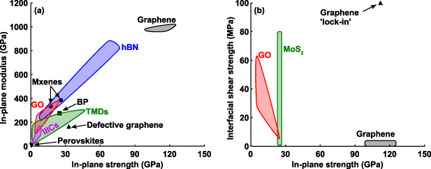
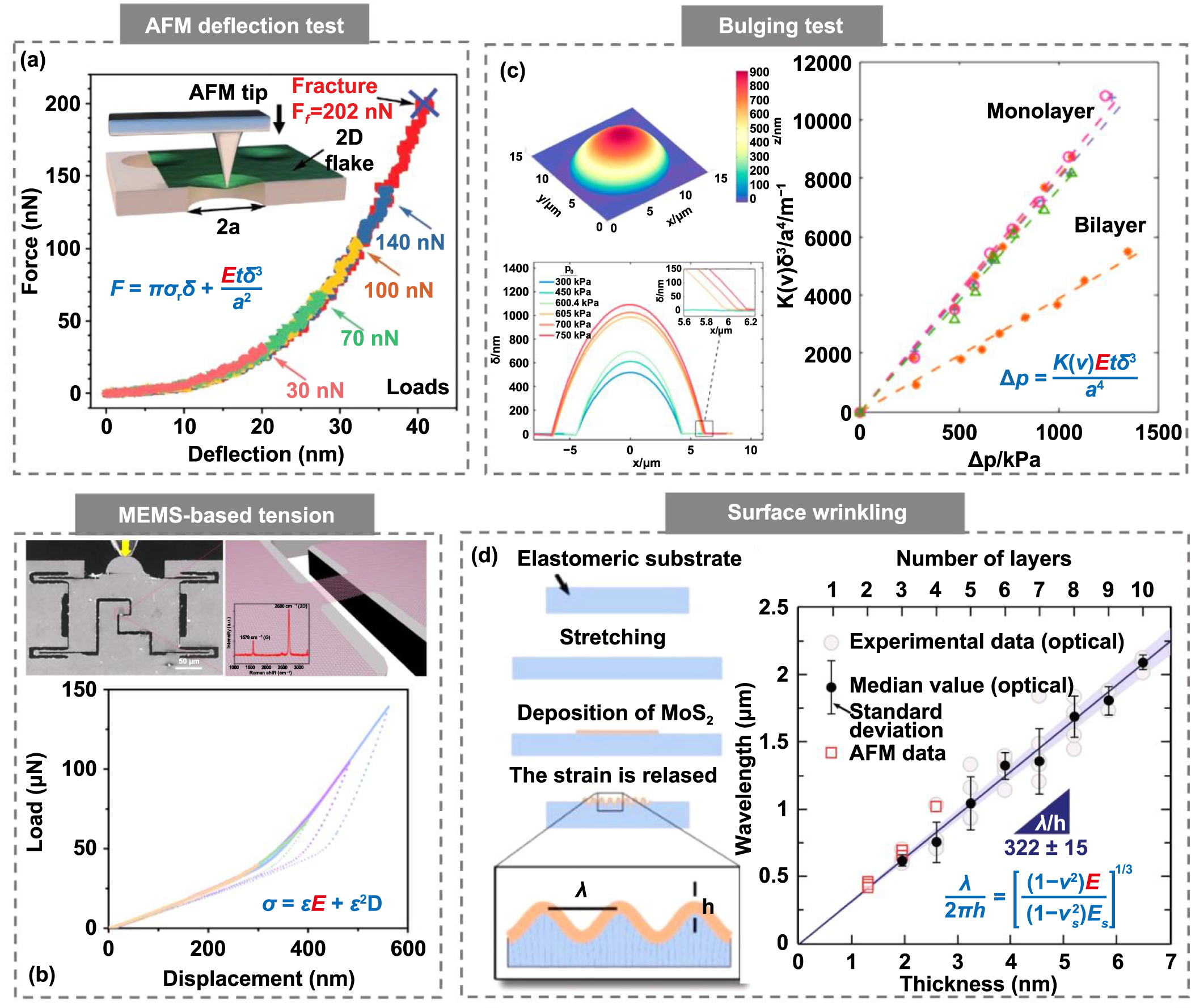
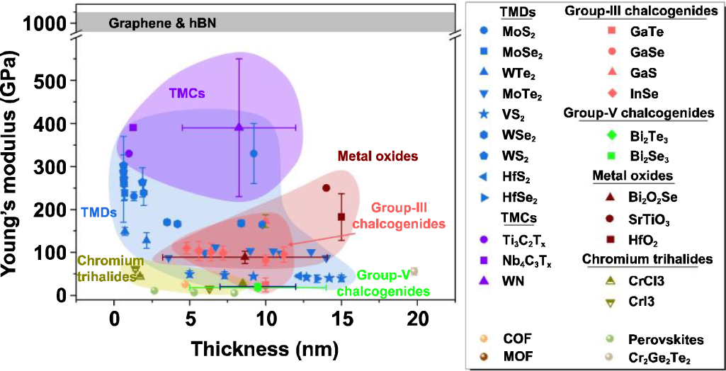
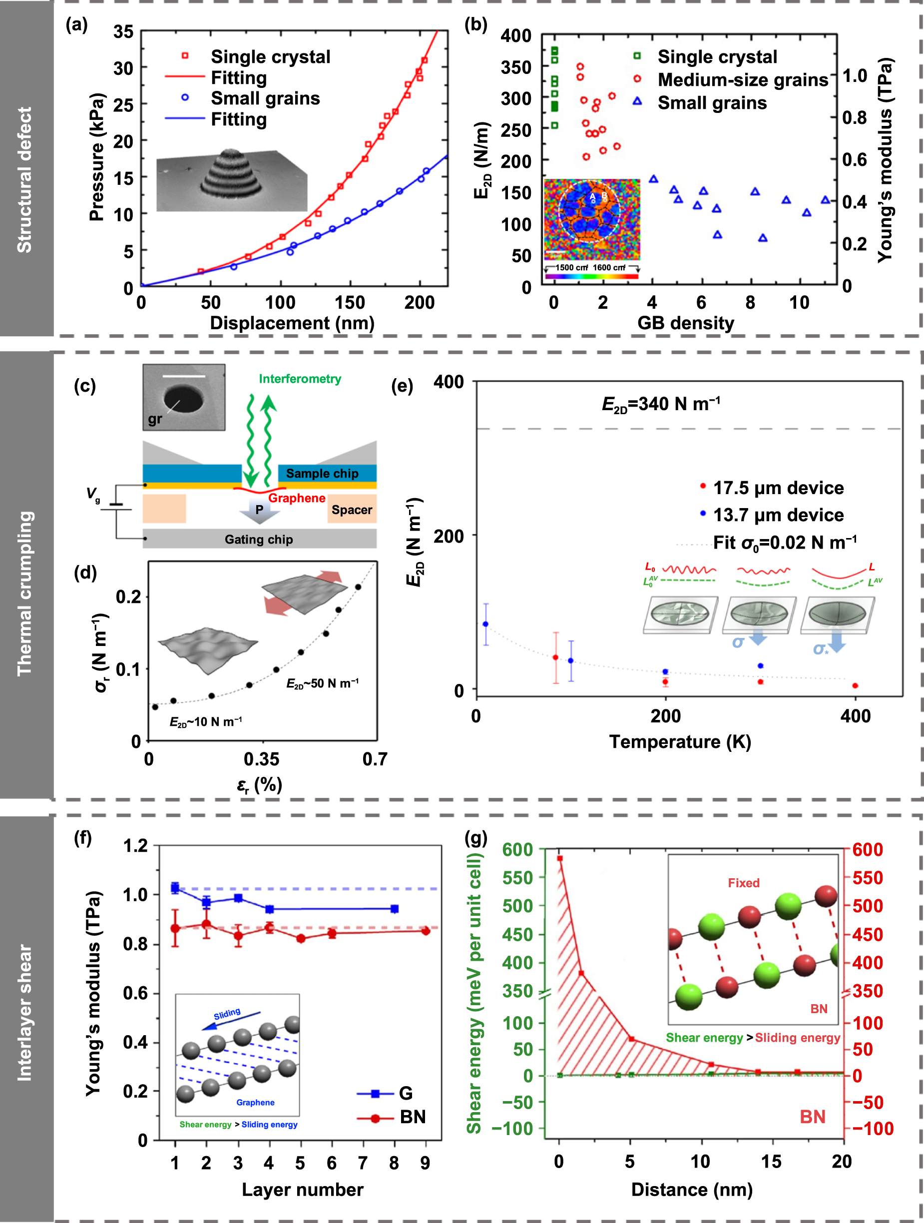
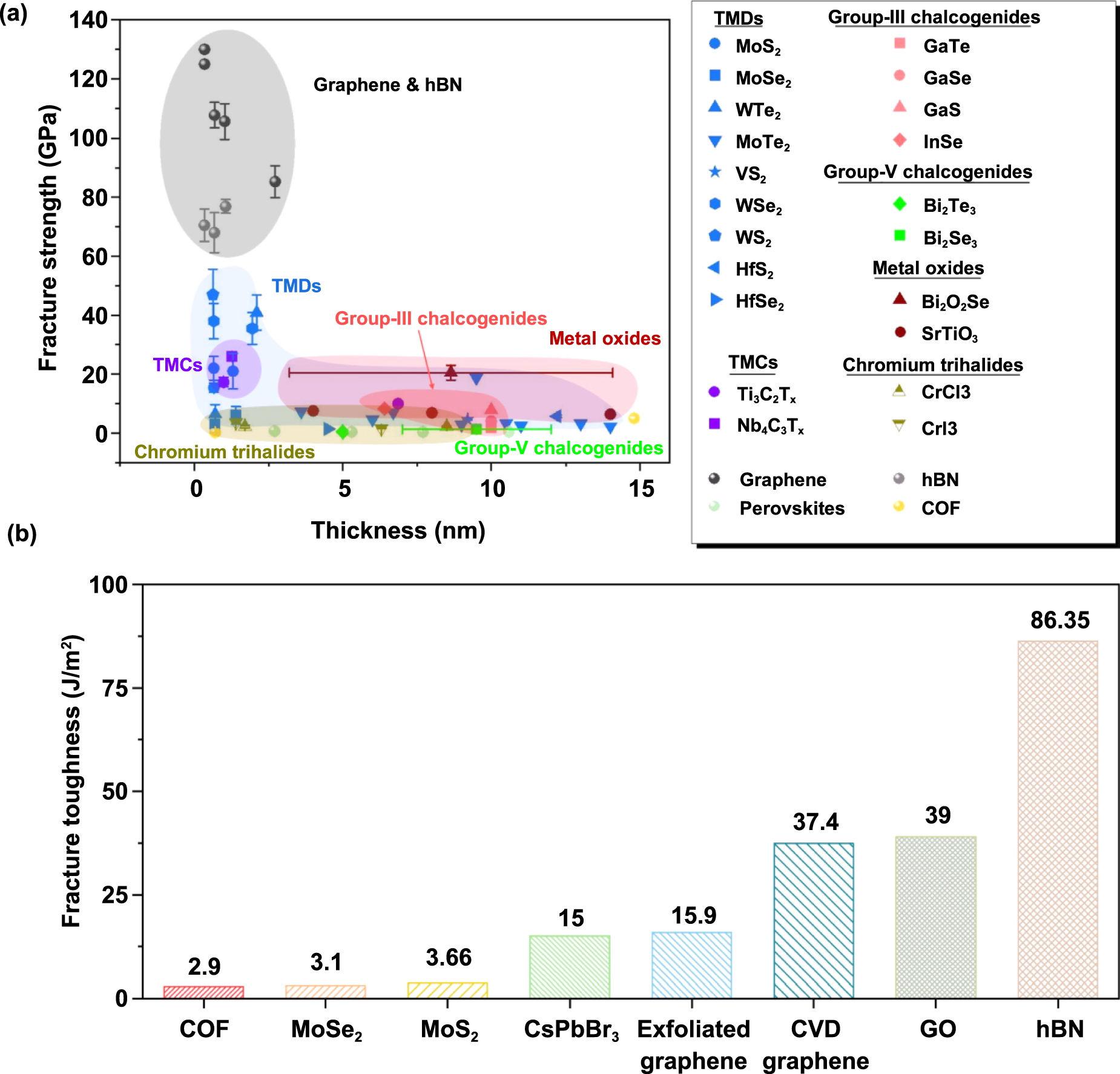
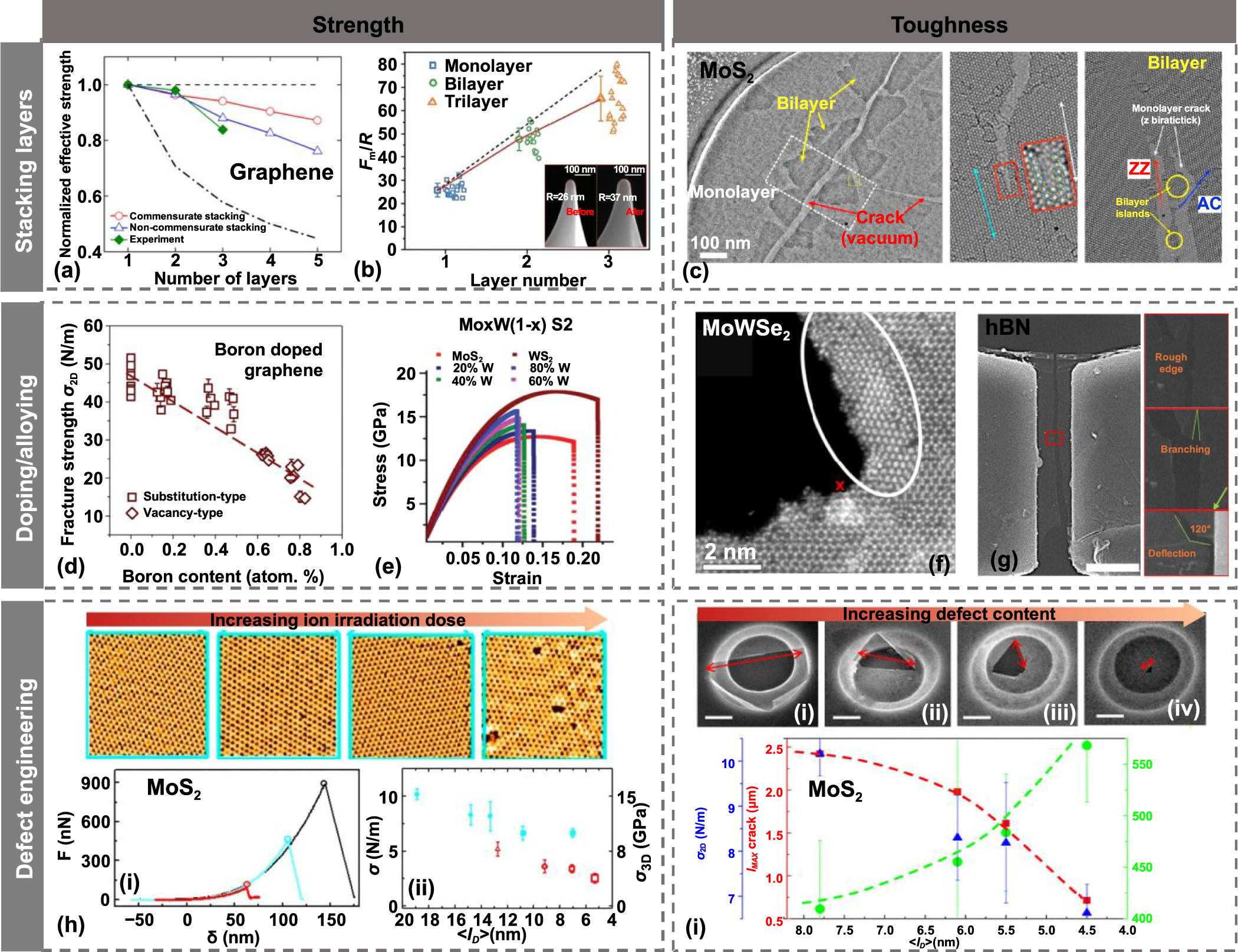
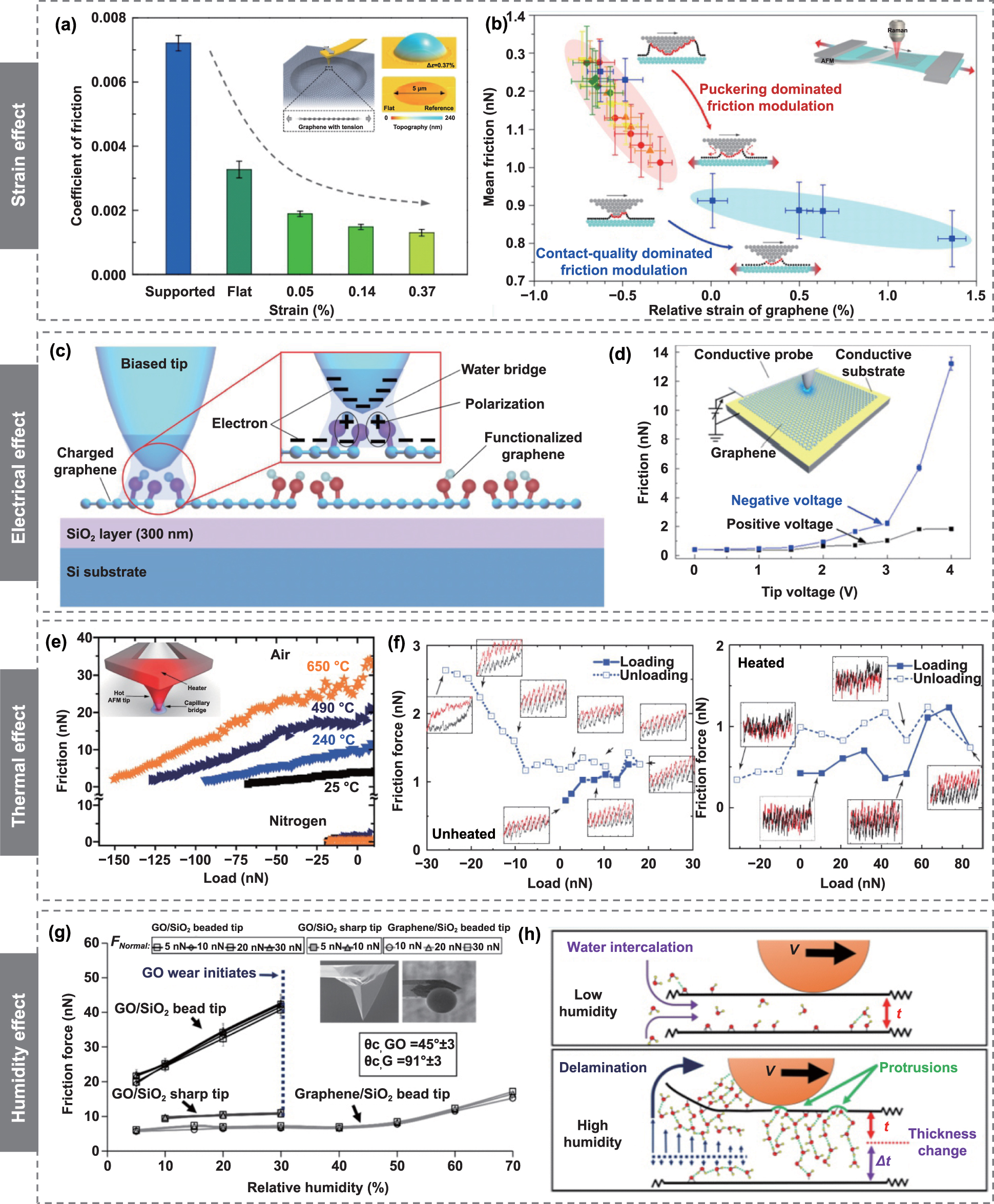
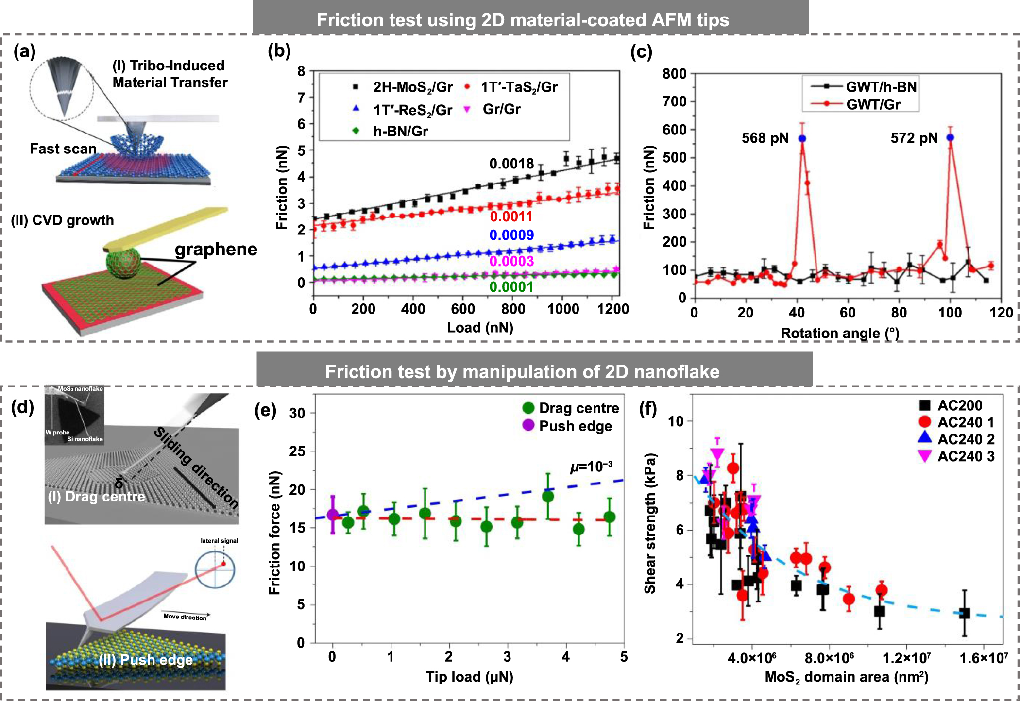
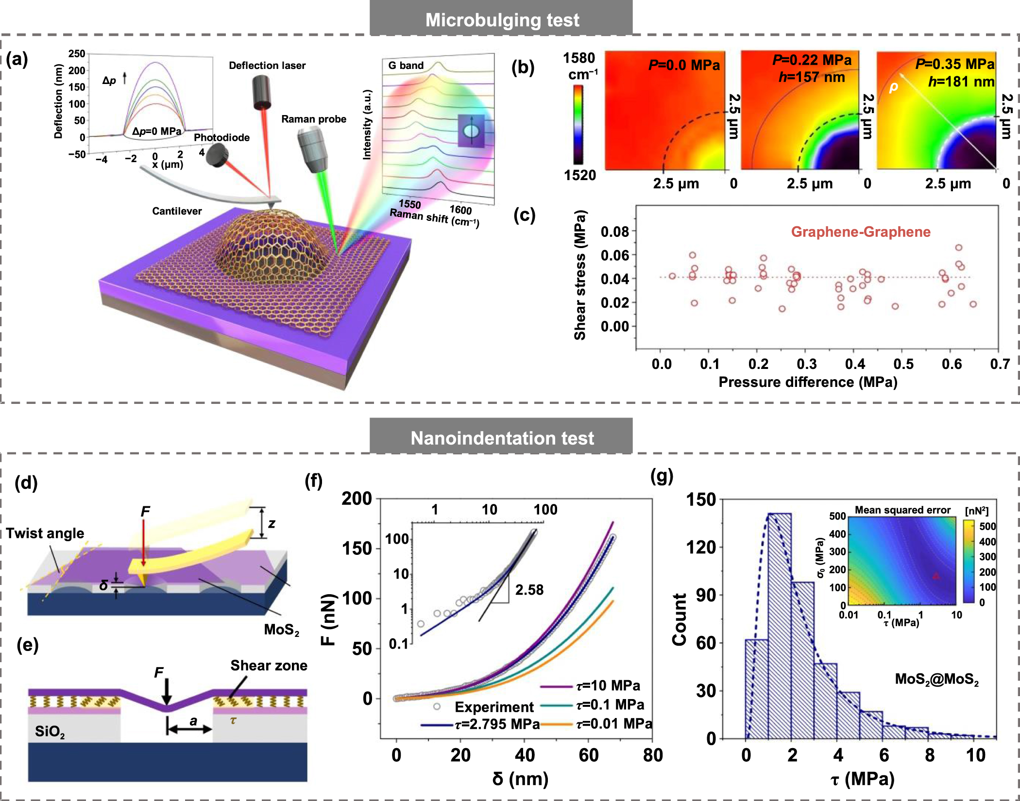
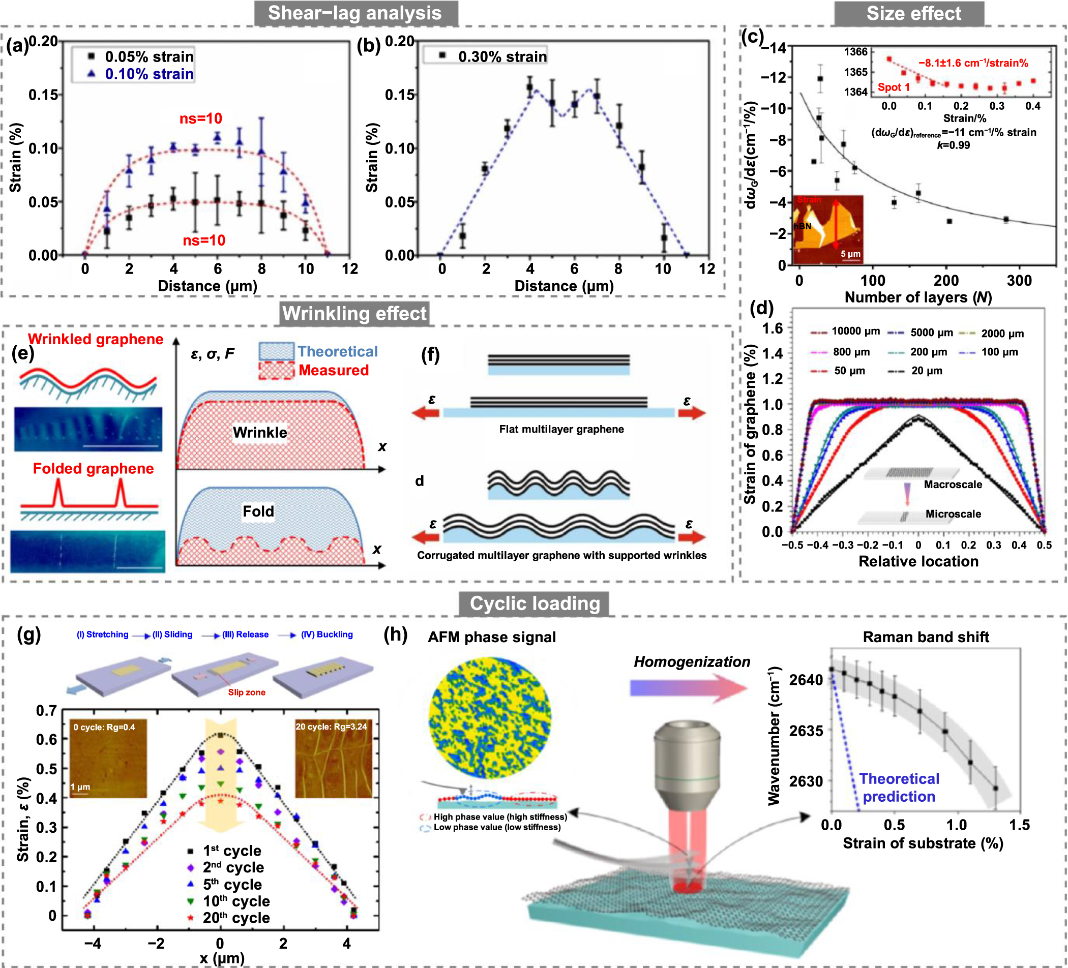
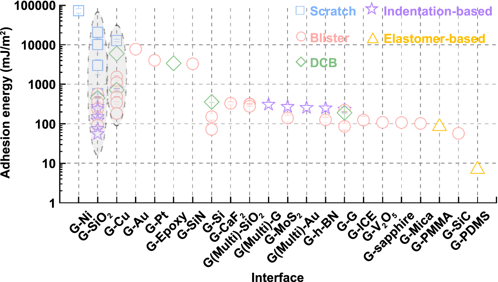
Figure 21. Plots illustrating the in-plane (a) and out-of-plane (b) mechanical properties of a collection of 2D materials. This data has been collected from the following references: graphene [19, 20, 29, 45, 163, 305, 385–387], graphene oxide [5, 7, 8, 337], TMDs (MoS2 [82, 118, 386, 388–392], MoSe2 [36], MoTe2 [139], WS2 [121], WSe2 [121, 123], WTe2 [121], HfS2 [124], HfSe2 [124] and VS2 [125]), hexagonal boron nitride [29, 160], black phosphorus [393], group III chalcogenides [130, 134] (IIICs), MXenes [112, 126], and perovskites [129]. In many systems, data in the literature is still sparse, which is particularly evident in measurements of the interfacial shear strengths.
Download figure:
Standard image High-resolution image
The out-of-plane strength, taken here as the interfacial shear strength between monolayers of the same material, are compared to the in-plane strength in figure 21(b). While measurements of friction at heterointerfaces are plentiful in the literature (e.g. as in AFM tip—2D FFM measurements, or in vdW heterostructures), the data on interfacial shear strength between 2D monolayers of the same material (i.e. homostructures) remains sparse. Here, data is organized to show the bounding behaviors across all literature values, as self-contained studies from the same research groups on the in-plane and out-of-plane strengths are largely unavailable (except in the case of GO [5, 7, 8, 27, 337]). In comparison to many of the in-plane properties, a wide degree of scatter exists in the measurements of interfacial shear strengths for many systems (notable graphene and MoS2) and underscores the large degree of uncertainty that remains in the mechanical properties of many 2D systems. Indeed, reports of 'lock-in' states due to commensurate contact between stacked 2D monolayers can lead to a dramatic increase in the interfacial shear strength, with the most notable report shown for graphene from Dienwebel et al [387]. In addition to structural sources, variability in interfacial shear strength measurements arises from differences in interlayer chemistry. For instance, the link between interfacial shear strength and the degree and form of functionalization of carbon monolayers has been well-demonstrated for GO [27, 337]. Finally, ambient humidity offers another source for variability in interfacial shear strength, which has been observed in both GO [337] and MoS2 [389, 392]. The degree of scatter in the interfacial properties reported in the literature underscores the importance of standardized testing methodologies in the measurement of the mechanical properties of 2D systems.
7.2. Outlook for experimental characterization and computational methodologies
Substantial efforts have been made in the experimental investigation of the mechanical properties of 2D materials through various techniques discussed in this review. As an outlook for future studies, a few topics of interest are proposed as follows.
Current research on the mechanics of 2D materials beyond graphene is still in its nascent stage, especially for newly emerging materials such as MOFs and COFs. While the unique dimensionality of these systems offers well-ordered structures to explore their structure-mechanics relationship at different domain size levels, their mechanical properties are currently underexplored. The preparation of freestanding, high-quality and large-area membranes or films is required for a more detailed mechanical characterization of this class of 2D materials.
In addition to COFs and MOFs, while a number of TMDs, such as MoS2, WS2, MoSe2, and WSe2, have been widely studied, few mechanical investigations have been performed on other TMDs (e.g. VS2, MoTe2, TaSe2, etc), and TMD alloys which exhibit unique chemical, electronic and magnetic properties. 2D heterostructures can be designed and built either by manual- or self-assembly techniques in vertical or lateral fashions [117]. These in-plane and vertical 2D heterostructures possess sub-nanometer thicknesses, offering great opportunities for engineering functional devices at the atomic and nanoscale level. The atomically sharp interfaces between different phases not only endow 2D heterostructures with exceptional electronic and photonic properties, but also define their overall mechanical behavior by accommodating lattice deformation via interfacial load transfer. There is, however, a dearth of information concerning the mechanical behaviors of 2D heterostructures. Moreover, Janus materials are an emerging class of 2D heterostructure, whose mating faces are either asymmetrically functionalized or exposed to a different local environment, thus presenting opposing properties and functionalities [394–396]. However, most related works are still computational, possibly due to difficulties in sample preparation.
Beyond 2D material systems, we believe opportunities exist in the dynamic testing space. Currently, most mechanical studies of 2D materials focus on the static or quasi-static performance, while the dynamic behaviors in response to cyclic loading or impact loading are largely unexplored. From an application's perspective, this gap in the literature is significant as dynamic properties are vital to durability and reliability of 2D material systems. For example, laser-induced supersonic projectile impact testing revealed an excellent impact resistance performance in multilayer graphene [397]. The high strain rate response of multilayer WSe2 was also examined by high-energy laser shock, generating nanoscale kinks due to the high pressure-induced bending and shearing [398]. To better understand the dynamic mechanical properties of 2D materials, theoretical models and relevant key parameters need to be developed to provide quantitative descriptions. From the perspective of methodology, new experimental techniques are required to give more comprehensive information of the deformation and failure mechanisms. For example, aberration-corrected TEM offers atomic-resolution imaging capability for the precise characterization of structural evolution of 2D materials under loading, allowing the intrinsic structure–property relationship to be established. Moireé patterns formed due to lattice mismatch or twisting of bilayers further can be leveraged for atomic-scale strain mapping based on Moiré interferometry analysis. Energy dispersive x-ray spectroscopy and electron energy loss spectroscopy under TEM imaging are able to identify the chemical and electronic structure of 2D materials, which is beneficial for the mechanical-chemical-physical coupling studies.
Finally, in addition to the force fields, many other physical fields simultaneously influence the mechanical properties and interfacial behavior of 2D materials in practical applications. Therefore, future efforts can focus on the mechanics-coupled multi-physics of 2D materials. In particular, the rapid development of thin-film and precision MEMS techniques allows 2D materials to be probed and engineered inside electron microscopes under external stimuli such as thermal, electrical, mechanical, optical, and magnetic fields at the nanoscale. In addition, the multimodal features endow AFM with versatility and multifunctionality for the study of external fields, including conductive mode, piezoelectric mode, magnetic mode, scanning thermal mode, and so forth. Meanwhile, environmental control is also enabled to investigate influences of temperature, humidity, service environment on the mechanics of 2D materials, which we anticipate will gain more interests from both the scientific and industrial communities.
As the mechanical property space of 2D materials continues to be charted by new experimental measurements, opportunities have emerged to harness the expanding knowledge of the mechanics of these systems. In this regard, strain engineering of functional properties presents an inevitable next-step in the study of 2D materials. Indeed, a number of studies have already demonstrated interesting strain-modulated behaviors in 2D materials including, band gap tuning [399, 400], thermal transport [401], and phase stability [249], among others. Despite some early progress in strain engineering topics, non-trivial challenges remain. For instance, experimental methods to apply controlled, multiaxial loadings to 2D materials represent an open issue. Nonetheless, the appetite for this research direction is strong within the community, as evidenced by recent opinions and reviews on this topic [284, 402]. We anticipate that maturity in the mechanics of 2D materials will elicit increased interest in strain engineering topics in the coming years.
The practical challenges in the handling and experimental testing of ultrathin systems reinforce the value of accurate computational methodologies to screen the vast mechanical property space of 2D materials. While DFT simulations offer a pathway to study the mechanics of these systems using first-principles approaches, the high computational cost and limitations on simulation size limit the application of this method to complex 2D systems (e.g. multilayers and heterostructures). MD-based simulations greatly increase the accessible length-scales but present their own challenges in the limited availability of interatomic potentials for 2D materials. Machine learning presents a new opportunity to create interatomic potentials for 2D systems without the need to develop deep domain expertise in each system of interest. Reports of 2D material interatomic potentials using machine learning techniques are nascent in the literature [23–26, 110, 111]. We anticipate further growth in this research direction to meet the growing need for MD-level simulations of a wide library of 2D material systems.
Acknowledgments
The authors acknowledge financial support from the Natural Sciences and Engineering Research Council (NSERC) of Canada, National Natural Science Foundation of China (Grant Nos. 12202430, 12241202), USTC Research Funds of the Double First-Class Initiative (Grant No. YD2090002011), and the China Scholarship Council.