

Abstract
Micro light-emitting diode (micro-LED) will play an important role in the future generation of smart displays. They are found very attractive in many applications, such as maskless lithography, biosensor, augmented reality (AR)/mixed reality etc, at the same time. A monitor that can fulfill saturated color rendering, high display resolution, and fast response time is highly desirable, and the micro-LED-based technology could be our best chance to meet these requirements. At present, semiconductor-based red, green and blue micro-LED chips and color-conversion enhanced micro-LEDs are the major contenders for full-color high-resolution displays. Both technologies need revolutionary ways to perfect the material qualities, fabricate the device, and assemble the individual parts into a system. In this roadmap, we will highlight the current status and challenges of micro-LED-related issues and discuss the possible advances in science and technology that can stand up to the challenges. The innovation in epitaxy, such as the tunnel junction, the direct epitaxy and nitride-based quantum wells for red and ultraviolet, can provide critical solutions to the micro-LED performance in various aspects. The quantum scale structure, like nanowires or nanorods, can be crucial for the scaling of the devices. Meanwhile, the color conversion method, which uses colloidal quantum dot as the active material, can provide a hassle-free way to assemble a large micro-LED array and emphasis the full-color demonstration via colloidal quantum dot. These quantum dots can be patterned by porous structure, inkjet, or photo-sensitive resin. In addition to the micro-LED devices, the peripheral components or technologies are equally important. Microchip transfer and repair, heterogeneous integration with the electronics, and the novel 2D material cannot be ignored, or the overall display module will be very power-consuming. The AR is one of the potential customers for micro-LED displays, and the user experience so far is limited due to the lack of a truly qualified display. Our analysis showed the micro-LED is on the way to addressing and solving the current problems, such as high loss optical coupling and narrow field of view. All these efforts are channeled to achieve an efficient display with all ideal qualities that meet our most stringent viewing requirements, and we expect it to become an indispensable part of our daily life.

Original content from this work may be used under the terms of the Creative Commons Attribution 4.0 license. Any further distribution of this work must maintain attribution to the author(s) and the title of the work, journal citation and DOI.
List of acronyms
| ACF | Anisotropic conductive film |
| ALD | Atomic layer deposition |
| AR | Augmented reality |
| CLC | Cholesteric liquid crystal |
| CQDs | Colloidal quantum dots |
| CC | Color conversion |
| CFs | Color filters |
| CSE | Confined selective epitaxy |
| DBR | Distributed Bragg reflector |
| DQWs | Double-quantum-wells |
| DPT | Dynamic pixel tuning |
| XR | Extended reality |
| EQE | External quantum efficiency |
| FOVs | Field of views |
| FRET | Fluorescence resonance energy transfer |
| FWHM | Full-width at half maximum |
| GaN | Gallium nitride |
| HEMTs | High electron mobility transistors |
| ITO | Indium-tin oxide |
| IQE | Internal quantum efficiency |
| LBS | Laser beam scanning |
| LISA | Laser interferometric space antenna |
| LEDs | Light emitting diodes |
| LOP | Light output power |
| LEDs | Light-emitting diodes |
| LCD | Liquid crystal display |
| LCoS | Liquid-crystal-on-silicon |
| MIGS | Metal-induced gap states |
| MOCVD | Metalorganic chemical vapor deposition |
| MOVPE | Metalorganic vapor-phase epitaxy |
| µLEDs | Micro light-emitting diode, microLEDs, micro-LEDs |
| MR | Mixed reality |
| MBE | Molecular beam epitaxy |
| NP | Nanoporous |
| NLOS | Non-line-of-sight |
| OLEDs | Organic light-emitting diodes |
| PPD | Pixel per degree |
| PPI | Pixel per inch |
| PECVD | Plasma-enhanced chemical vapor deposition |
| QDs | Quantum dots |
| QE | Quantum efficiency |
| QCSE | Quantum-confined Stark effect |
| RGB | Red, green and blue |
| SAM | Magnesium aluminate scandium oxide (ScAlMgO4) |
| SRH | Shockley–Read–Hall |
| SQW | Single-quantum-well |
| SRTs | Strain-relaxed templates |
| SLs | Superlattices |
| SMD | Surface-mounted device |
| TFT | Thin-film transistor |
| TJs | Tunnel junctions |
| 2D | Two-dimensional |
| UV | Ultraviolet |
| VCSEL | Vertical-cavity surface-emitting laser |
| VR | Virtual reality |
| VLC | Visible light communication |
| WPE | Wall-plug efficiency |
| WDM | Wavelength division multiplexing |
1. Introduction to the micro-LED roadmap
Chien-Chung Lin1, Yuh-Renn Wu1 and Hao-Chung Kuo2,3
1Graduate Institute of Photonics and Optoelectronics, National Taiwan University, Taipei 10617, Taiwan
2National Yang Ming Chiao Tung University, No. 1001, Daxue Road, East District, Hsinchu City 300093, Taiwan
3Semiconductor Research Center, Hon-Hai Research Institute, Taipei, Taiwan
Status
One of the breakthroughs in the last century is the invention of the semiconductor based light emitting devices, including lasers and LEDs. While the first observation of visible photons from the semiconductor diode junction was made in 1962 [1], the realization of the full-color semiconductor based light emitting devices waited for several decades later [2]. The adaptation of GaN based material opened a whole new direction from the traditional III–V group of elements and thus started the development of semiconductor based UV/blue/green colors LEDs [3–7]. In the early 1990s, high-power application of LEDs was the main stream due to the imminent demand for solid-state lighting. Meanwhile, some researchers found a different potential of these highly-efficient devices and started working on their miniaturization [8–10]. Like previous display technologies, the micro-LED-related display has modest beginnings. The intrinsic issues of the device, such as carrier diffusion into sidewall [11] and sidewall surface passivation [12–14] need to be overcome, and the benchmark/comparison from other more mature technologies can be a tough battle to fight. Since then, tremendous efforts and our demand for a better viewing experience have been the driving force behind it. The semiconductor-based LEDs address human's demand in the information display: high brightness, saturated color, high frame rates, and high resolution. To achieve these, we have seen a rapid growth in terms of research results. Figure 1 shows the number of publications extracted from the Internet (source: https://app.dimensions.ai/discover/publication). The actual number of papers that are closely related to micro-LEDs can be located in between these two curves. From its humble start, we saw an increase of 81 times in 20 years and corresponding to 5-year CAGR of 68.2% recently. The fast growth of publication indicates the attention that the micro-LED gathers is enormous.

Figure 1. The number of published paper by year is shown. Two different search criteria were applied: one is limited to the micro-LED is included in the title while the other one is that the word 'micro-LED' showing up anywhere in the full text.
Download figure:
Standard image High-resolution imageIn addition to scientific interests, we also noticed the rise of related applications, including commercialization of micro-LED-based TV, and outdoor signage installations. The bright color and smooth animation from the semiconductor chips catch viewers' attentions and we believe more penetration into the consumer market is possible in the next decade. On the other hand, the extension towards other non-display applications is also very likely happening. The sensor integration will be essential to put micro assembly and IoT into the big picture [15]. The individually addressable pixel illumination can bring the maskless photolithography possible [16]. The non-toxic nature of the GaN based micro-LED can find its way into the medical examinations [17, 18]. As we can see here, these just exemplified the immense opportunity brought by the micro-LEDs.
Meanwhile, micro-LED technology is still developing and has many barriers. From the material growth, the device design, the display module, the assembly technique, and the system integration, many technical fields that exist today need to be upgraded or even revolutionized to handle the accuracy and the performance that are required by the micro-LED panel. This is the main reason why we edit this roadmap. There are many problems that need to be sorted out and many of them are not easy to tackle. Complicated problems need solutions that could revolutionize the whole field in the next few years and bring impacts to our daily life. By bringing the experts' opinions, we can see a clearer direction ahead and work together to achieve our goals.
Roadmap organization and goals
In the following, we will briefly introduce three important categories in this roadmap. Micro-LED-related products are now under intense research and development, and many prototypes or even initial commercialization can now be seen in major market. The whole supply chain was established long time ago when the SMD based LED display started. However, the current industries' throughput and accuracy are not enough to meet the demand for the micro-LED-based panel. Many procedures and the technologies associated with them must adapt to the specifications' quantum jump.
Material and devices: This part includes the material growth and device design that could have a fundamental breakthrough for micro-LEDs. Due to the requirements of the smart display, the resolution needs to be increased beyond 1000 PPI in many applications. So the ultimate goal on the device is to have micron-level fabrication for the three primary colors (RGB). This goal will need epitaxy improvement over the current capability, for example, the wavelength variation across the wafer needs to be controlled within 2 nm or less. How to design the wafer epitaxial layers before the growth is also a good direction to enhance the chances of success. The forward voltage issues in nitride-based green and red LEDs are also important, where the V-defects and the reduction of the piezoelectric field with the InGaN barrier are studied [19]. The inclusion of TJ solved the spectral utilization for a semiconductor-based solar cell in the past, and many efforts have been put into realizing the TJ in a micro-LED wafer which can eventually replace the absorbing transparent oxide layer in the p-type contact.
Another direction of development for the sub-micron devices is to have the optimized nano-rod/nano-pillar/nano-wire structure for the device. The nano-scale rod or wire structures can also be potential candidates for the sub-micron device. For both GaN and traditional III–V material (GaAs, InP), many examples were demonstrated [20–23].
Although the light emitting capability is usually what we focus in the micro-LED development, the importance of electronic driver cannot be overlooked. In addition to the traditional poly-Si, transparent oxides, novel materials such as graphene and MoS2 start to make their way into this application. The availability of large area growth and transfer of 2D material, corresponding ohmic contact, and further high-density layout and integration can be the backbone of the high-resolution micro-LED display.
Full-color rendering in micro displays : One of the benefits of the semiconductor-based micro-LED is the wide-span coverage of emission colors. From ultra-violet to deep red, different active materials can be applied, including AlGaN, InGaN, AlGaInP, etc. While various colors are fascinating, these materials do pose different problems in the fabrication. Among these materials, AlGaInP was used (and is still used) for red-color devices, while InGaN can be applied for blue and green color generation. Their performances towards size reduction are quite different. AlGaInP-based devices are more susceptible than InGaN's when the device size is reduced to 5 μm or less. Thus the InGaN quantum well with red-emission is one of the newly developed fields that could be an important step for the full-color display in one material system.
We have to point out that there is another method to realize full-color rendering, i.e. through the CC method where the high energy photons provided by the micro-LEDs can be transformed into other primary colors (like red or green). Colloidal quantum dots have been the front runner as the major conversion material in this method. However, these nanocrystals are usually not easy to be patterned. Especially when we have to integrate these material with the micro-LED arrays. Different designs or methods have been introduced to achieve this goal. From the photo-sensitive quantum dot resin, inkjet-style precision spray, to NP structure to embed quantum dots, we saw numerous methods to provide us a better solution to realize a full-color micro display.
Micro-LED issues addressed in system/modules: In addition to the inherent device performance, the integrated system that combines various parts into one platform plays a crucial role for adaptation of micro-LEDs. The AR goggle can be viewed as an example for the integration. The micro-LEDs need to be small and powerful enough to be able to overcome the environmental light source (such as the Sun). Meanwhile the resolution is also key because now the monitor is too close to our eyes and the requirement of resolution rises rapidly.
Equally important to the system performance is the ability to mass transfer and repair of the micro-LED system. Since the early stage, people have recognized the importance of these technologies and they are regarded as the bottleneck of the whole supply chain at one time. The applicable methods are many: elastomer stamp, mechanical pick and place, laser assisted releasing, electromagnetic force, roll-to-roll printing by stretchable film, etc. The yield and the throughput can hold the key to commercial success. When the pixel number exceeds beyond a million, everything including repair, becomes time-consuming if we cannot find an efficient way to accomplish the job. Higher the transfer yield, less the repair time is needed, and this seems to be the eventual guidance when the industry looks into this product seriously.
Concluding remarks
Finally, we can use figure 2 as a summary for this roadmap. The whole supply chain of a micro-LED system (as shown in figure 2(a)) covers many industries and shall incorporate more in the years to come. Before the LCD became popular, there was a long development time and huge efforts were undertaken by our predecessors [24]. We believe similar trend shall be followed by this brand new micro-LED technologies. There are many aspects need to be addressed to achieve a mature, cost-effective, and highly efficient micro-LED technology as we can see in figure 2(b). In this roadmap, we intended to discuss the technological development and the future of these aspects. Many works have been done, and more will emerge before we can really put this topic into everybody's home.

Figure 2. (a) A simplified supply chain model for a micro-LED system and the scope of this roadmap. (Source: Industrial Technology Research Institute, Taiwan). (b) The conceptual visualization of what a good micro-LED technology should be. Most of the topics are discussed in this study.
Download figure:
Standard image High-resolution imageAcknowledgement
This work was financially supported by the National Science and Technology Council, Taiwan under the Contract Nos. MOST 110–2221-E-002-186-MY3, and MOST 111–2218-E-A49-019-MBK.
2. MicroLEDs with high efficiency
Matthew S. Wong1, Steven P. DenBaars1,2 and Shuji Nakamura1,2
1Materials Department, University of California, Santa Barbara, CA 93106, United States of America
2Department of Electrical and Computer Engineering, University of California, Santa Barbara, CA 93106, United States of America
Status
Micro-LEDs have gained tremendous research attention due to their emerging applications that are beyond conventional illumination, such as in displays, visible-light communication, and optogenetics [25–27]. Some of the inherent features of conventional LEDs including high energy efficiency, excellent chemical robustness, and outstanding brightness are the potential advantages of micro-LEDs over other light emitters. Among all the micro-LED features, their high energy efficiency is presumably the most appealing aspect for many commercial products. However, the micro-LED efficiency is usually contrasted by the epitaxial design and fabrication processes, and is typically not limited by the material quality or device design like standard LEDs for general lighting application. The impacts of SRH non-radiative recombination increase with decreasing device dimensions or increasing the ratio of sidewall perimeter to light-emitting area, where the SRH non-radiative recombination sites are attributed to surface recombination and sidewall damage from dry etching [28]. Although surface recombination and sidewall damage exist in LEDs in all sizes, they have greater influences to smaller devices as the device dimensions are approaching to the minority carrier diffusion length of the semiconductor material systems [29, 30]. One of the main consequences from surface recombination and sidewall damage is the reduction of maximum EQE in small micro-LEDs, which is commonly known as the size effect [28, 29, 31]. We, at the University of California, Santa Barbara (UCSB), have been developing simple and effective methods, including the use of wet etching at the sidewalls and followed by ALD for dielectric sidewall passivation, for recovering the peak EQE of InGaN- and AlGaInP-based micro-LEDs by addressing the surface recombination and sidewall damage issues, as shown in figure 3 [12, 31–34]. The sidewall treatments that are used to the efficiency of micro-LEDs have been examined by other researchers, which show the straightforward nature and rapid adoptability of our methods. In addition to the device improvements, the micro-LEDs with sidewall treatments also demonstrate better reliability and longer operating lifetime [13]. Since the size effect in micro-LEDs have been significantly investigated and tackled, after employing the sidewall treatments to eliminate the size effect, the efficiency limitation and variation of micro-LEDs are dependent on the material quality, material growth uniformity, and the epitaxial designs or structures of LED wafers. In the next sections, the anticipated device development roadmap for micro-LEDs will be discussed. With the annihilation of the size effect using the effective and mature device fabrication techniques, the importance on the epitaxial and material developments, namely III-nitride devices for long-wavelength emission and TJs grown by MOCVD, will be explored.

Figure 3. The progress in improving the peak EQE of 20 × 20 µm2 InGaN and AlGaInP micro-LEDs at UCSB. The EQE ratio is relative to the corresponding 100 × 100 µm2 devices with indium tin oxide (ITO) contact.
Download figure:
Standard image High-resolution imageCurrent and future challenges
Conventional visible LEDs composed of LEDs with two material systems, where III-nitride materials cover in blue and green wavelengths and AlGaInP system provides very energy-efficient red emission. Long-wavelength emission, particularly in red emission, has been a challenge for III-nitride devices since the success of blue LEDs [35]. The difficulty for realizing long-wavelength emission is attributed to the material quality in the active region. GaN and InN have 10% lattice mismatch that makes high indium InGaN layer challenging. As the emission wavelength approaches toward red, greater indium composition is required in the active region, where low-temperature growth is required and high strain is introduced. The cause of low-temperature growth and strain results in poor InGaN material quality and low luminous efficiency, hence low efficiency performance of conventional III-nitride red LEDs has been observed in the literature [36]. The realization of red, green, and blue micro-LEDs using one material system is greatly desired for monolithic integration for display applications. Monolithic integration of red, green, and blue III-nitride micro-LEDs is expected to make device fabrication, heterogenous integration, and mass transfer processes more straightforward and effective, which the complexity in fabrication and integration is one of the main disadvantages for using both InGaN and AlGaInP micro-LEDs. To make monolithic integration successful for practical applications, III-nitride red emission with high efficiency is essential. Although further optimizations are necessary to realize energy-efficient III-nitride red emitters, it is important to demonstrate III-nitride red micro-LEDs can give as good optical and electrical characteristics than AlGaInP micro-LEDs and other types of red emitters, if not better. Among all the perspectives of III-nitride red LEDs, the color purity and electrical efficiency are the major parameters to optimize for displays, the most important potential application for micro-LEDs. To date, color purity has not been getting a lot of attention when conducting investigations on III-nitride LEDs, while color purity is one of the crucial metrics when comparing different display technologies. Color purity is governed mainly by two factors of an emission spectrum: the emission wavelength and the emission bandwidth, also known as the FWHM. Both the emission wavelength and the emission bandwidth affect our color perception, where the emission wavelength controls the hue and the emission bandwidth impacts the saturation, hence these two parameters are the key optical components for III-nitride red micro-LEDs. While most of the research focuses on the pushing the emission wavelength value towards red emission wavelength range (⩾630 nm), the need to obtain narrow emission bandwidth has given limited attention.
From the monolithic integration aspect, TJs play a critical role to the red, green, and blue tandem LEDs design where at least two TJs are needed. Traditionally, TJs have been a great interest for III-nitride optoelectronic devices, such as laser diodes and LEDs, due to the high optical transparency in UV and visible wavelengths, which enhances the light extraction efficiency. Conductive and transparent oxides, such as ITO or zinc oxide, are traditionally employed for current spreading layer due to the resistive characteristic of p-type III-nitride materials, yet ITO has greater absorption in blue and UV emissions. TJs not only offer benefit in better optical transparency but also reveal the possibility of the cascade LED design that achieves monolithic integration of multiple emission wavelengths or suppress the efficiency droop issues [37, 38]. TJs have been demonstrated by MBE, a hydrogen-free deposition method, and significant improvements in optical efficiency has been shown. Nevertheless, MBE requires ultrahigh vacuum and hard to scale up for mass production, resulting in cost-ineffective TJs grown by MBE compared to ITO. In order to make TJs cost effective and manufacturable, MOCVD is necessary. The main challenge for TJs grown by MOCVD is the resistive electrical characteristics of the device, since MOCVD is hydrogen-rich reactor where the hydrogen passivates the p-type layer [34]. The main challenge for TJs grown by MOCVD is p-GaN activation after the formation of TJ, which n-GaN or the n-side of TJ, acts as a barrier for hydrogen diffusion. Other than the activation issue, InGaN insertion layer is commonly used to reduce the electrical penalty by increasing the tunneling probability due to the lower tunneling barrier. However, this InGaN insertion method could attribute to significant light absorption for visible and UV light emitters, especially in the tandem design.
Advances in science and technology to meet challenges
As mentioned in the previous section, due to the lattice mismatch between InN and GaN, the active region of III-nitride red emitters exhibits high tensile strain that results in poor material growth and device performance. In recent years, several novel growth techniques have been demonstrated to enhance long wavelength emission by using strain engineering, such as SRTs [39, 40]. Because of their small sizes, micro-LEDs have advantage in suppressing strain unlike their larger counterparts. Moreover, novel growth techniques that utilize strain engineering have been developed to allow 100% biaxially relaxation [39]. For many approaches that realize red emission, including SRT, InGaNOS, and porous GaN, a strain-relaxation layer or buffer is formed before the subsequent growths of the LED structure, where substrate patterning is often required before LED growth. In the SRT method, no substrate patterning is needed and the strain-relaxation layer is composed of the decomposition of an InGaN layer, which the decomposed InGaN layer appears to be dark in the resulting SRT samples. The SRT method enables uniform growth across full 2-inch wafers and the growth of active region at significantly higher temperature at 825 °C compared to conventional growth methods. Moreover, the 20 × 20 µm2 red micro-LEDs fabricated on SRT yielded the lowest forward voltage between 2.00 V and 2.05 V at 20 A cm−2 in the literature, suggesting that this method is more energy efficient than other approaches in the literature. The potential reason for the low forward voltage could be attributed to the use of v-pit engineering that leads to a more effective hole injection to the active region, yet further experimental analysis is necessary to understand the strain-relaxation mechanism in SRT. Because SRT provides a SRT, this technique can be applied for other types of optoelectronic devices that suffer from the strain effect, such as AlGaN-based deep UV light emitters. Although the SRT method shows promising device performance with red emission, the state-of-the-art EQE characteristic remains low compared to the record blue and green counterparts, and additional material and processing optimizations, such as substrate removal, are necessary to achieve high efficiency III-nitride red LEDs. As there are various approaches on pushing the emission wavelength towards red color in recent years, it is crucial to consider other optical aspects that are specific for display applications, for example color saturation, and tailor the micro-LED structure and device design to accommodate with the display specifications while offering excellent brightness and energy efficiency.
For MOCVD TJ development, in addition to the challenges in TJ growth and design, the p-GaN activation plays a critical role in the electrical characteristic. For micro-LEDs with TJ contacts grown by MOCVD, several activation methods, including activation via sidewalls and selective-area growth of TJs, have been demonstrated to facilitate hydrogen diffusion out of the passivated p-GaN. It has been shown that the activation conditions, such as annealing temperature and activation approach, have strong impacts to the optical and electrical performances [41]. Because of the small device sizes, the distance of hydrogen diffusion is comparable to the device dimension, where sidewall activation can be effective to result in great electrical characteristic. It has been shown that 20 × 20 µm2 micro-LEDs with TJ contact have better peak EQE, as well as maximum WPE, than the device with ITO contact by employing chemical treatment before thermal activation via sidewalls, as shown in the year 2021 data point of figure 3, which is the first demonstration that micro-LEDs with MOCVD TJ contact can outperform ITO devices in terms of EQE and WPE [34]. The better efficiency is attributed to greater optical power, but the current-voltage characteristic of the TJ device requires more attention to reduce the voltage penalty compared to the ITO device [41]. It is anticipated that the activation processes will become more mature and develop to address the voltage penalty issue in MOCVD-grown TJs, and the activation mechanism can be further understood via empirical and simulation work. Other than the activation method, the TJ design also serves as an important factor to increase the efficiency of micro-LEDs. Besides the conventional doping optimizations for better tunneling probability, approaches that utilize bandgap engineering within the TJ architecture would be beneficial to improve the electrical characteristics of MOCVD-TJ devices. In traditional III-nitride TJ contacts, because of the wide bandgap nature of GaN, InGaN insertion layer is used to lower the tunneling barrier and to reduce the voltage penalty. Nevertheless, this typical approach decreases the voltage penalty by increasing the indium incorporation in the InGaN insertion layer, leading to a lower optical transparency of the TJs. Therefore, innovative ways to address the voltage penalty challenge without sacrificing the optical advantage of TJ is necessary. Recently, a new TJ design that utilized AlGaN/GaN polarization charges to enhance the TJ performance, where the polarization charges resulted in additional band bending and shorter tunneling distance [42]. Since this AlGaN/GaN TJ design was InGaN-free, the EQE and the LOP remained identical as GaN TJ, yet the WPE and the electrical characteristic were improved. This AlGaN/GaN TJ approach has several potential benefits in terms of material growth and versatility compared to the traditional InGaN insertion layer method. The growth of high indium composition of InGaN layer with excellent crystal quality has always been a challenge for III-nitride optical devices, whereas the growths of AlGaN on GaN are relatively straightforward. Moreover, the AlGaN/GaN TJ design can be applied in other optical devices as a transparent current spreading layer, such as UV light emitters and VCSELs, due to the low optical absorption of AlGaN/GaN. The research on TJs, with the focus on high optical transparency in the deep UV and visible light wavelength range, is expected to become more important in the future as the traditional current spreading layer cannot satisfy the need of various emerging optoelectrical devices, including UV light emitters, monolithic micro-LEDs, VCSELs, and single photon emitters. Although the developments of III-nitride TJ began in early 2000s, the use of TJs did not gain significant attention due to the availability of alternative current spreading techniques in conventional blue/white LEDs, such as flip-chip design and transparent and conductive oxides. With the new III-nitride optical devices become more mature, it is anticipated that the use of TJs will be a critical component in these futuristic devices with excellent device performance and efficiency.
Concluding remarks
High efficiency is one of the most important metrics for micro-LEDs to enable various potential applications. For micro-LEDs, the efficiency relies on both the material and the fabrication perspectives, since the device performances are affected by not only the material quality but also the size effect due to surface recombination and sidewall damage. The size effect has been investigated significantly and methods have been proposed to address this issue. The material aspect will be critical for future studies to enhance the efficiency of III-nitride micro-LEDs.
Acknowledgements
This work was funded by the Solid-State Lighting and Energy Electronics Center (SSLEEC) at the University of California, Santa Barbara (UCSB). A portion of this work was performed in the UCSB nanofabrication facility, an open access laboratory.
3. Nano-wire/nano-rod structure for micro LEDs
Ayush Pandey and Zetian Mi
Department of Electrical Engineering and Computer Science, University of Michigan, 1301 Beal Avenue, Ann Arbor, MI 48109, United States of America
Status
Emerging technologies such as AR and VR demand resolutions, stability and brightness that current displays based on organic LEDs, conventional inorganic LEDs and LCDs cannot provide. In this context, smaller devices such as micro-LEDs and nanoLEDs can replace these technologies due to them combining the advantages of inorganic LEDs, with a smaller size approaching to micrometer, or even submicron scales. However, as shown in figure 4 [43], the EQE of conventional quantum well LEDs drops when the device dimensions are scaled down below a critical dimension. The resulting efficiency cliff, i.e., a drastic reduction of the device efficiency with reducing dimensions, has remained an unresolved challenge for the market adoption of micro-LEDs. The critical dimension of efficiency cliff corresponds to approximately a lateral size of 10 to 100 microns. The underlying challenges include the presence of extensive defects and dislocations caused by etching of conventional quantum well LEDs and the resulting nonradiative surface recombination and current leakage paths. Moreover, it has remained extremely difficult to achieve high efficiency green and red emission utilizing conventional InGaN quantum wells even for broad area LEDs, due to the large lattice mismatch between indium-rich InGaN and GaN, strain-induced phase separation, and QCSE [35, 44].

Figure 4. Variations of peak EQE of some previously reported III–V visible LEDs with different lateral sizes. Our results are shown as stars, with the color of the star corresponding to the device emission color. © [2022] IEEE. Reprinted, with permission, from [43].
Download figure:
Standard image High-resolution imageRecent studies have shown that these critical challenges can be addressed, to a certain extent, by III-nitride nanowire/nanorod structures. Early studies of nanowires had been focused on spontaneous formation via chemical vapor deposition. With the recent advances of selective area epitaxy, device-worthy III-nitride nanocrystal arrays, with precisely controlled size, spacing, morphology, and polarity can be grown directly on foreign substrates [22, 45, 46]. The emission wavelengths can be varied from UV, through visible to the near-infrared [47]. The emission wavelengths can be further varied by controlling the nanocrystal lateral dimensions, leading to multi-color emission for nanowire LEDs grown on a single substrate in a single epitaxial step [48]. By precisely controlling the size and spacing, III-nitride nanowire arrays can form photonic crystal, or metasurface structures, leading to enhanced QE, narrow spectral linewidth and directional emission [49, 50]. An InGaN photonic crystal nanowire green micro-LEDs with a spectral linewidth of 4 nm has been demonstrated, which is nearly one order of magnitude smaller than that of conventional quantum well LEDs [51]. More recently, high efficiency (EQE up to 25%) N-polar InGaN/GaN nanowire green and red LEDs, with lateral dimensions as small as 0.7 µm, has been demonstrated directly on wafer without any packaging [52–54].
Current and future challenges
The decrease in efficiency of micro-LEDs for smaller device sizes is largely due to the surface damage induced during the fabrication of the device mesa, which is typically done using a plasma etch [28]. Nanostructures have several advantages over conventional planar layers, especially for micro-LEDs, where the mesa etch step can be circumvented, preventing the sidewall damage that affects top-down devices. However, there have been few reports on efficient optoelectronic devices using them, despite their excellent optical quality. This is largely due to the high leakage currents and surface recombination in these devices, which are partly related due to the fabrication of devices, where it is extremely difficult to fully insulate the gap between nanowires. The fabrication process is particularly challenging for nanowire LEDs grown by MOCVD, which often have a lateral p–i–n configuration. With the recent advances of vertical nanowire p–i–n LED structure by MBE and the development of core-shell heterostructures, significantly improved performance has been reported for long-wavelength (green and red) micro-LEDs. For example, during the growth of InGaN/GaN quantum well/disk active region, the incorporation of aluminum in the quantum barrier layer can lead to the spontaneous formation of an Al-rich AlGaN shell surrounding the LED active region, which can significantly reduce nonradiative surface recombination and leakage currents [55]. Most work on nanostructures has also been focused on spontaneous nanowires having mixed polarity, and the more common Ga-polar orientation, where the tapered top morphology and uneven nanowire height aggravates the difficulties in fabrication. While the nanowire morphology depends on the polarity, the uneven height is a result of the random nucleation during the initial phases of growth.
For high-efficiency and high-power LEDs, it is essential to minimize the efficiency droop. As the electron concentration and mobility are significantly higher than for holes in the III-nitrides, there is a large imbalance in the electron and hole injection to the active region. This results in electron overflow out of the active region, reducing device efficiency at high currents. The polarization fields in the layers also result in a shift in emission wavelength with changing current, which can impact the perceived color of emission, limiting their operation range. Further, while III-nitrides are used for blue to green emission, AlGaInP is used for red emission in displays. This makes their integration into a pixel quite challenging, especially as the pixels are also required to have specific dimensions and spacing. Usually this is done using a pick-and-place method [56]. However, the transfer of individual devices, and the subsequent identification and repair of defective devices is an extremely time-consuming and expensive process.
Advances in science and technology to meet challenges
Recent work has shown that nanostructures can be used to grow highly efficient small-area LEDs. Using SAG on substrates with well-defined polarity results in highly uniform nanowires with the same polarity, eliminating the non-uniformity associated with spontaneous nanowires. ALD has been used to passivate the nanowire sidewalls, while simultaneously filling the gaps in between nanowires, eliminating the possibility electrical shorts. These advancements have greatly increased the yield, reliability, and performance of nanowire-based devices. Shown in figure 5, by varying the nanowire dimensions, full-color emission can be achieved for nanowire LEDs grown on a single chip in a single epitaxial step [57].

Figure 5. (a) Schematic illustration of a monolithically integrated multi-color single nanowire micro-LED pixel. (b) EL spectra of single nanowire LEDs with different nanowire diameters (D). © [2022] IEEE. Reprinted, with permission, from [43]. Reprinted with permission from [57]. Copyright (2016) American Chemical Society.
Download figure:
Standard image High-resolution imageIt is highly desired that micro-LEDs can exhibit stable emission across a large current range and possess a narrow spectral linewidth, which, however, has remained challenging due to indium phase separation and QCSE. To overcome this problem, photonic crystal structures can be fabricated to limit the emission to a single dominant mode. SAG offers a viable route to grow such structures, as has been shown for green micro-LEDs, down to an area of ∼3 µm2. The devices exhibited highly directional emission, with a stable emission peak at ∼548 nm over several orders of injection current [51], shown in figure 6(a). Significantly, the spectral linewidth stays at a nearly constant value of 4 nm over a large range of injection currents, which is nearly one order of magnitude smaller than conventional InGaN quantum well LEDs. TJ has also been incorporated into micro-LEDs to increase the injection of holes into the active region, reducing the efficiency droop [58]. An efficiency of 5.5% was measured at 3.4 A cm−2 for such a device directly on wafer, with an area of only 3 µm × 3 µm, and the efficiency droop was 30% at an elevated injection current of 28 A cm−2, shown in figure 6(b).

Figure 6. (a) Electroluminescence spectra of an InGaN/GaN photonic nanocrystal micro-LED measured under varying injection current at room temperature. (b) Variation of the relative external quantum efficiency (EQE) vs. injection current density. Reprinted from [51], with the permission of AIP Publishing. © [2022] IEEE. Reprinted, with permission, from [43].
Download figure:
Standard image High-resolution imageN-polar InGaN/GaN nanowire arrays have been shown with emission covering the visible spectrum. The N-polar orientation results in a flat top surface morphology for nanostructures, that is easily compatible with fabrication technologies, and previous work has shown that the reversed polarization fields can reduce the impact of electron overflow from the device active region [59]. For growing nanowires with strong red emission, an in-situ annealing method was developed, through which the nanowire luminescence could be increased by an order of magnitude [52]. Devices were fabricated by using Al2O3, deposited by ALD, and a thick SiO2 layer deposited by PECVD, to cover the nanowires, into which submicron injection windows were etched to reveal the nanowire top surfaces. The fabricated devices exhibited record high EQE, measured on-wafer, of 11% for green [53] and 2.2% for red [52] submicron LEDs. Some of the device characteristics are shown in figure 7.

Figure 7. (a) I–V characteristics of a submicron InGaN/GaN nanowire LED. The inset shows a top-view SEM image of the current injection window for a micro-LED device. (b) Representative EL spectra of a N-polar submicron-LED. The inset shows an optical microscopy image of a micro-LED operating under room light illumination. Variations of (c) output power and (d) EQE with current density for a high-efficiency green micro-LED. Reproduced with permission from [53]. © [2022] IEEE. Reprinted, with permission, from [43].
Download figure:
Standard image High-resolution imageConcluding remarks
III-nitride nanostructures have shown tremendous promise to overcome the critical limitations of top-down processes for growing and fabricating micron-scale and even smaller optoelectronic devices, thereby providing a viable path to address the efficiency cliff of micro-LED technology. Such dislocation-free nanostructures can further enhance the performance and functionality of micro-LEDs, including narrow spectral linewidth and highly directional and stable emission. Long-wavelength (red and green) emission from InGaN suffers from a lack of spectral purity due to the large full-width half-maximum and the peak wavelength shift with injection current [60]. The nanowire arrays can be appropriately modified to enhance the photonic crystal effect, which can ensure extremely stable luminescence peaks, with narrow linewidth and highly directional emission. The design of the nanowire heterostructure can also be modified to incorporate TJs, further improving efficiency and reducing droop. This method can be adapted to define nanostructures of specific dimensions to target emission at different wavelengths, as has been shown previously [57], enabling pixels containing individual wires with different color emission from a single growth. This would avoid the cumbersome mass transfer techniques used in typical display technologies.
In the near future we envision the development of nanowire-based based pixels that can span the entire visible spectrum, grown in a single step. This would allow for the realization of dense arrays, which can form the foundation of future display technologies. Such devices could also harness the excitonic nature of recombination in nanowires for improving the device efficiency, as has been shown recently [54, 61, 62]. The versatility of nanowires also enables their development on different substrates, which would also be of great importance for biological and biomedical applications of micro-LEDs. Furthermore, nanowires can also be used to develop photonic crystal vertical surface-emitting lasers, that would have applications in VLC. The unique advantages of the bottom-up growth technique are therefore well-suited to the realization of high-performance optoelectronic devices.
Acknowledgements
This work was supported by NS Nanotech, Inc.
Conflict of interest
Some IP related to this work has been licensed to NS Nanotech, Inc., which is co-founded by Z Mi. The University of Michigan and Mi have a financial interest in NS Nanotech.
4. UV micro-LEDs and applications
Pengfei Tian
School of Information Science and Technology, Fudan University, Shanghai 200433, People's Republic of China
Status
Since the demonstration of high-efficiency blue LEDs by Shuji Nakamura, GaN-based LEDs with emission wavelength from red to UVC (200–280 nm) have been widely researched especially for low-cost and high-efficiency general lighting. Recently, the effective COVID-19 inactivation by UVC LED stimulates the fast development of UV LEDs. Compared with broad-area LEDs, AlGaN UV micro-LEDs with typical size from 1 μm to 100 μm have advantages of array format, better current spreading, lower thermal effect, higher sustainable current density, higher modulation bandwidth, higher light extraction efficiency, and higher density of LOP, which can address fundamental device or system issues and thus open up more applications. Figure 8 summarizes the applications of broad-area UV LEDs such as air disinfection, curing, sensing and photo therapy, as well as the advanced UV micro-LED applications including micro-LED display, optical communication, maskless photolithography, time-resolved fluorescence detection and charge management [63].

Figure 8. Various UV LED and micro-LED applications at different wavelengths and optical powers. © [2022] IEEE. Reprinted, with permission, from [63].
Download figure:
Standard image High-resolution imageMicro-LED display has attracted significant attention for its advantages over LCD and OLED display techniques. But the industry has been facing difficulties to fabricate low-cost large-area full-color displays, and commonly used techniques are transfer printing, CC and material growth [64]. Combining UV micro-LEDs with CC materials to obtain full-color display shows possible advantages of high pixel density, uniform driving condition and relatively easy processing. RGB quantum dots (QDs) usually have higher absorption coefficients in the UV range than the visible light, so this approach also suggests possible high display efficiency and uniform emission RGB spectra. The QD CC efficiency excited by short UV light may suffer from non-radiative recombination loss, as well as reflection, scattering, and coupling loss, which need to be optimized for such approach.
Solar-blind UVC optical communication has no ambient light interference and may achieve NLOS communication. UVC micro-LED has higher modulation bandwidth than broad-area LEDs and further reducing the device size causes higher bandwidth. UVC micro-LED communication has achieved record data rate of 4 Gbps at a distance of 5 m [65]. WDM combining UVA, UVB, UVC and even visible light will further improve the data rate significantly [66, 67]. Shorter wavelength UVC light can be strongly scattered for optical communication in air enabling possibilities of NLOS communication. Although single UVC micro-LED delivers limited LOP, but UVC micro-LEDs in series or parallel will alleviate such effect and high-sensitivity single photon counting can be employed to increase the detection sensitivity given almost no background noises at the solar-blind range.
UV micro-LED based maskless photography uses direct writing to achieve image patterns on photoresist, which requires no traditional hard mask and reduces the cost and complexity compared with traditional lithography. Parallel direct writing, high-resolution, multi-step alignment, and portable system are also further advantages which have been developed by Dawson's group [68]. Another application of UV micro-LEDs is time-resolved fluorescence detection, which can provide advantages of low-cost, compact, spatial resolution, and easy adjustment of micro-LED wavelength [69]. We are also expecting more application potential after addressing a few key issues of UV micro-LEDs.
Current and future challenges
UV micro-LEDs are expected to demonstrate significant advantages of high efficiency, high reliability, fast modulation speed, low cost and low-power consumption. However, the EQE of UV LEDs is still low, especially below 20% at UVC range [63, 70]. The crystal quality by MOCVD growth, high-quality p-type AlGaN layer, UV light absorption inside the UV LED device are typical limiting factors, and researches of UV micro-LED efficiency are far less than visible micro-LEDs, e.g. sidewall defect effect. The low efficiency, high series resistance of UV devices and other factors are detrimental to the high reliability of UV devices.
High-speed UV micro-LEDs have been reported in recent years showing high modulation bandwidth of hundreds of MHz, but the bandwidth is still lower than the maximum value of GHz of the visible light micro-LEDs, especially for the short-wavelength UVC devices. The bandwidth is determined by the carrier lifetime and resistance-capacitance effect, which is related to the high-quality UV material and device design. Similar to the high-bandwidth micro-LEDs, fast UV micro-LEDs with ultra-short light pulse are necessary for time-resolved fluorescence detection.
In the future, further improvements in the UV micro-LED efficiency, reliability and speed will be necessary for applications in display, optical communication, direct writing, fluorescence detection, charge management etc. System design of current and future novel applications based on UV micro-LEDs also appear to be challenges to be resolved.
Advances in science and technology to meet challenges
High-quality material growth and device fabrication are the first step to conquer these challenges. UV LED structure have been optimized to increase the IQE and light extraction efficiency [63]. Mg-delta doping and Mg-doped SL have been employed to increase the p-doping efficiency in AlGaN. The p-type ohmic contact and hole concentration are improved by growing p-GaN layer on p-AlGaN layer. The series resistance can be further reduced by optimizing the n-type doping AlGaN and ohmic contact. UV micro-LED have better current spreading, lower thermal effect and higher light extraction efficiency, so researchers have fabricated a large micro-LED array to form high-efficiency broad-area UV LEDs [71]. Through reducing the UV micro-LED size, etching inclined micro-LED sidewall and using Al reflection layer, TM-polarized emission may be enhanced to increase the light extraction efficiency. Smaller UVC micro-LED with higher EQE have been experimentally and theoretically proven [72].
UV micro-LED lifetime, especially for short-wavelength UVC micro-LED, can be strongly degraded at high injection current densities due to the high defect density during growth and generated defects during operation. Therefore, we could adopt a few approaches to increase the reliability, e.g. reducing the defect density for epitaxial growth, designing high-efficiency device structures and developing effective thermal management. Moreover, for a UV micro-LED array, one micro-LED can be used as photodetector to detect the adjacent micro-LED emission intensity through the waveguide effect of the n-AlGaN. The reduction and fluctuation of the UV light intensity could be reflected by the excited photocurrent, so we have the opportunity design a feedback circuit to stabilize the emission intensity [73].
UV micro-LED array can lead to more revolutionary applications besides those mentioned above. Electron charge accumulation on the gold surface of the test mass of LISA may affect the test accuracy of space-based gravitational wave detection. The electron charge level can be effectively controlled by UVC light [74]. The low-power consumption, precise adjustment of low LOP at pW level, high modulation speed, the relatively high efficiency and high reliability make UVC micro-LED suitable for charge management application. The integration of UV micro-LED emitter and photodetector offers an opportunity to develop integrated on-chip communication and UV spectrophotometer for gas sensing. The array format and the electronic interfacing to complementary metal-oxide-semiconductor (CMOS) lead to miniaturized systems so more applications of UV micro-LED can be further explored.
Concluding remarks
UV micro-LED with array format has demonstrated significant advantages of high efficiency, high reliability, low power consumption, and high modulation bandwidth, and many groups have demonstrated its applications in micro-LED display, optical communication and maskless photolithography. In the future, material growth, device fabrication, and advanced packaging of the UV micro-LED array need to be improved to further increase the efficiency, reliability and modulation bandwidth, especially in the UVC wavelength range. Upon such technology progresses of the UV micro-LEDs, we can expect more applications of UV micro-LEDs in fluorescence detection, charge management, sensing and more advanced applications.
Acknowledgements
This work was supported by National Key Research and Development Program of China (Project No. 2021YFC2202500, Task No. 2021YFC2202503). I would like to acknowledge valuable discussions with Na Gao, Li Liu and Erdan Gu.
5. InGaN-based red micro-LEDs
Kazuhiro Ohkawa and Daisuke Iida
King Abdullah University of Science and Technology, CEMSE Division, KAUST, Thuwal 23955-6900, Saudi Arabia
Status
InGaN and AlGaInP are candidates for red micro-LEDs. Standard-sized, AlGaInP-based red LEDs are widely used in many applications (e.g. traffic signals). However, miniaturizing AlGaInP red LEDs is challenging due to surface carrier recombination on their sidewalls. The surface recombination velocity of AlGaInP is greater than that of GaN [75]. AlGaInP red (peak wavelength (λp)≈ 632 nm) micro-LEDs with a size of 20 × 20 μm2 exhibit a LOP density of 175 mW cm−2 [2]; the LOP density of InGaN-based red micro-LEDs has increased from 40 to 176 to 936 mW cm−2 in recent years [76–78]. After just one year, the LOP density of InGaN red micro-LEDs was five-fold that of AlGaInP red micro-LEDs. That improvement was made possible by advances in LED structures and micro-device processing.
LED structures rely on strain control techniques such as strain relaxation to introduce more In [79] and strain compensation to maintain high crystallinity [80], which results in high-quality high-In-content InGaN layers as the active region. Figure 9 shows an LED structure grown by MOVPE on a c-plane sapphire substrate. The blue InGaN SQW and GaN/InGaN SLs lead to a high rate of In incorporation into the red InGaN DQWs via strain relaxation. The InGaN red DQWs consist of high-In-content InGaN wells and AlGaN/AlN barriers to compensate for the biaxial strain in the c-plane, which maintains the high quality of the red InGaN DQWs [80].

Figure 9. Top-down view of InGaN-based red micro-LEDs (17 x 17 μm2) with (a) and without (b) current injection. (c) Cross-sectional transmission electron microscopy (TEM) image of a single micro-LED device. (d) The InGaN-based red LED structure. Reproduced from [77]. CC BY 4.0.
Download figure:
Standard image High-resolution imageFigure 9(a) shows a 100-chip red micro-LED array. The peak wavelength of the array shifts from 662 nm to 630 nm in the cases of 10 A cm−2 and 50 A cm−2, respectively. The sidewalls of each LED were chemically treated; damaged sidewalls are characterized by a faster recombination velocity, which results in a non-radiative surface current. Chemical surface treatments effectively remove such damaged surfaces [32]. Pixelation via hydrogen passivation of p-GaN can produce RGB micro-LEDs as small as 4 μm [78, 81]. Hydrogen passivation is also useful for suppressing surface carrier recombination on the sidewalls to improve device performance [14].
Current and future challenges
InGaN red micro-LEDs are brand-new devices, and they are associated with many challenges such as achieving a longer peak wavelength, a narrower FWHM, and increased efficiency. This technology needs to mature before it is suitable for widespread usage (e.g. micro-LED displays).
There are three major challenges associated with InGaN red micro-LEDs can be summarized as follows:
- (1)Achieving a longer peak wavelength (⩾650 nm) and a narrower FWHM (⩽47 nm),
- (2)Suppressing a large blueshift of the peak wavelength with current,
- (3)Ensuring higher efficiency (e.g. one order higher than the current level).
According to the ITU-R Rec. 2020 standards (Rec. 2020), the apparent wavelength of red emission is 630 nm. Current InGaN red LEDs have broad FWHMs exceeding 45 nm [82]. Therefore, to meet Rec. 2020, the peak wavelength and FWHM of InGaN red LEDs should be at least 650 nm and less than 47 nm, respectively.
The temperature dependencies of the peak wavelength and intensity of InGaN red LEDs are very stable compared with those of AlGaInP red LEDs thanks to the larger conduction-band and valence-band offsets in the InGaN QWs. However, InGaN red LEDs exhibit large blueshifts, as described in the previous section, due to the strong QCSE in their QWs. Large blueshifts via QCSE make many applications more difficult.
The EQEs of InGaN blue and green LEDs can be as high as 80% and 50%, respectively. On the other hand, the EQEs of InGaN red LEDs are 5% at 632 nm [83, 84]. The EQEs of InGaN red LEDs have improved recently. However, there is still an order of magnitude difference between the EQEs of red LEDs and those of blue/green LEDs. Additionally, the spectral luminous efficiency functions for photopic vision (V(λ)) are 0.265, 0.710, and 0.060 at 632, 520, and 460 nm, respectively. The spectral luminous efficiencies of red (632 nm) and blue (460 nm) LEDs are much lower than those of green (520 nm) LEDs. Figure 10 shows the on-wafer LOP densities of RGB micro-LED arrays and their luminances as a function of current density. The LOP density was calculated by considering the emitting area. The LOP density and luminance of red micro-LEDs are 0.73 W cm−2 and 2.1 × 10⁵ cd m−2, respectively, at 100 A cm−2. In the case of a 5 μm-squircle red micro-LED, its area is 21.66 μm2 [81]. Therefore, the luminous intensity of one red micro-LED is only 4.5 μcd at 100 A cm−2. The LOP density of the blue micro-LED array was the largest in our RGB arrays, but its luminance was lower than that of the green micro-LED array due to its low spectral luminous efficiency. The RGB luminances of the RGB micro-LED arrays shown in figure 10 reveal that the efficiency of a red micro-LED array must be from three times to one order higher to be similar to those of blue or green micro-LED arrays.

Figure 10. Current density dependencies of on-wafer LOP densities (dashed lines with experimental data points) and the luminance (solid lines) for RGB micro-LED arrays.
Download figure:
Standard image High-resolution imageAdvances in science and technology to meet challenges
The three aforementioned challenges are not independent of one other. For example, If more In is incorporated into InGaN QWs to produce a 650-nm red LED, QCSE will be stronger and the InGaN crystallinity will be degraded. As a result, the LED will exhibit a larger blueshift and a lower EQE. Current red LED structures are characterized by (0001) c-plane growth on c-sapphire, Si (111), or c-GaN substrates, and the cladding materials on those substrates are GaN. Therefore, a significant biaxial compressive strain is present in high-In-content InGaN QWs embedded in GaN. That strain results in a large blueshift and a lower EQE due to the strong QCSE and the generation of defects. The following three advanced technologies hold promise for meeting the aforementioned challenges.
- (a)Strain-released templates
- (b)SAM substrates
- (c)Non-polar and semi-polar substrates
The UCSB group is already investigating strain-released templates by introducing porous regions [2]. It will accordingly be possible to reduce the QCSE, which will result in smaller blueshifts and higher efficiencies. However, the current red LEDs used on such templates exhibit broad spectral emission, which result in inhomogeneous strain in the InGaN. Additional technical progress is expected to be made in the coming years.
SAM is a novel substrate material. Its c-plane is lattice-matched with In0.17Ga0.83N [85]. Red LEDs on SAM substrates will have In0.35Ga0.65N QWs with In0.17Ga0.83N cladding layers, but bright red LEDs have not yet been reported. On the other hand, bright blue LEDs have already been achieved on SAM substrates [86], indicating that the integration of RGB LEDs on SAM substrates should be possible. The differences in In content between the QWs and cladding layers of red LEDs on SAM and those of blue LEDs on sapphire are similar, which translates into similar strains. It means that strain in red LED structures on SAM substrates is the same level as that in blue LEDs on sapphire substrates, resulting in similar QCSEs and blueshifts. Drastic improvements of InGaN on SAM are expected for efficient red LEDs within the next five years.
Non-polar and semi-polar nitride growths are attractive for eliminating or reducing the QCSE in InGaN QWs [87], which means zero or small blueshifts and higher EQEs in InGaN red LEDs. However, the nitride growth on those polarities is still challenging since non- or semi-polar substrates are not yet popular. Research opportunities remain limited despite the great potential of this technology; long-term development is necessary.
Concluding remarks
Progress in the development of highly-efficient InGaN-based red micro-LEDs and the integration of monolithic RGB micro-LEDs is crucial to ensure high-performance and low-cost micro-LED displays. There have been steady advances in shrinking InGaN-based red micro-LEDs and boosting their LOP density. Current devices are 5 μm or smaller. The LOP density of InGaN red micro-LEDs is five-fold that of AlGaInP LEDs. However, it is necessary to achieve a longer peak wavelength (⩾650 nm) and narrower FWHM (⩽47 nm) to meet Rec. 2020 standards. Moreover, drastic improvements in the blueshifts and efficiencies of red micro-LEDs are required in order to attain parity with blue and green micro-LEDs. The QCSE and defects induced by strain reduce an LED's efficiency. Therefore, strain-released templates will no doubt be the subject of short-term research, novel SAM substrates will be the focus of mid-term research, and non-polar and semi-polar growth will be the subject of long-term investigations.
Acknowledgements
Some of the results highlighted in this paper were financially supported by KAUST (BAS/1/1676-01-01).
6. Manufacturing microLEDs from the perspective of epi-growth: direct epitaxy
Tao Wang1, Yuefei Cai2 and Jie Bai1
1Department of Electronic and Electrical Engineering, The University of Sheffield, Sheffield S1 3JD, United Kingdom
2Department of Electronic and Electrical Engineering, Southern University of Science and Technology, Shenzhen 518055, People's Republic of China
Status
The development of III-nitride semiconductor emitters on a microscale initially aimed to discover new physical phenomena as such reduced device dimension may form microcavity effects, leading to enhanced spontaneous emission, improved QE or reduced lasing threshold. Until recently, III-nitrides based visible µLEDs have started to draw intensive attention in terms of practical applications due to an increasing demand of developing microdisplays for smartwatches, smartphones, televisions, and AR/VR devices. Especially, AR/VR devices are typically utilized at proximity to the eye, thereby requiring high resolution, high contrast ratio and high luminance, high EQE, where micro-LEDs can potentially meet these requirements due to their unique features in comparison with OLEDs and LCD [56, 88–91].
In principle, μLEDs falls into two categories in terms of practical applications: auto-display and next generation TV typically require μLEDs with a dimension of <100 µm, while the μLEDs with a dimension of <50 µm can meet the other applications as mentioned above. It is worth highlighting that AR/VR devices require the μLEDs with a dimension of ⩽5 µm.
Figure 11 illustrates schematically two main approaches to the fabrication of microdisplays using III-nitride based μLEDs. The 1st approach is the so-called pick-and-place technique [90], where individual blue and green µLEDs fabricated from III-nitrides wafers and individual red µLEDs from AlInGaP wafers are transferred onto a targeting substrate finally forming a full color display. Due to the natural restrictions which will be discussed later, the approach is typical used for the fabrication of a microdisplay based on μLEDs with a dimension of ⩾50 µm. The 2nd approach is based on a heterogeneous integration technique, integrating µLED arrays with arrays of transistors such as CMOS that provide active-matrix switching [91], where μLEDs with a dimension of <50 μm are used. Conventional dry-etching processes are used to define μLED mesas, naturally introducing surface damage which becomes increasingly severe with reducing the dimension of μLEDs. Therefore, the approach is generally limited to the fabrication of μLEDs with a dimension of >10 µm. To achieve a full color microdisplay using this approach, down-version materials such as quantum dots have to be used, posing the fundamental limitations due to the nature of the down-conversion processes [92].

Figure 11. Schematics of the pick-and-place approach (top) and the integration of µLED arrays with arrays of transistors (bottom) [90, 91]. [90] John Wiley & Sons. © 2016 Society for Information Display. Reprinted from [91], with the permission of AIP Publishing.
Download figure:
Standard image High-resolution imageCurrent and future challenges
The pick-and-place approach involves the transfer and then bonding of 100 million µLED chips from epitaxial wafers to a target substrate, where electrical connection and mechanical support are provided, leading to a yield issue due to the requirement of the precise pick-up and placement. Moreover, it is tough to employ this approach for μLEDs with a dimension of <50 µm. For the second approach stated above, where µLED chips can be integrated into a driving circuit such as CMOS by means of a flip chip technique, dry etching processes inevitably introduce severe surface damage, significantly enhancing non-radiative recombination rates [28] and then leading to a drastic reduction in EQE [30]. An ALD technique has been proposed for sidewall passivation [31]. However, the improvement is marginal.
AlGaInP red LEDs with a large area exhibit high EQE [93]. However, once AlGaInP wafers are fabricated into µLEDs, a massive reduction in EQE occurs due to the enhanced surface recombination rate and the long diffusion length of carriers [94]. It is ideal to manufacture a fully color display by using all III-nitride semiconductors given that the bandgap of an InGaN alloy across their entire composition covers the whole visible spectrum. However, it is naturally difficult to achieve high indium-content InGaN which is required to obtain red emission whilst maintaining high optical performance [95].
A full color microdisplay is currently fabricated using either complicated waveguides [96] or down-conversion materials [92]. The former requires many extra optical components leading to severe energy loss, while the latter suffers from energy loss and challenges in accurately positioning the down-conversion materials.
Advances in science and technology to meet challenges
To attempt to address the challenges mentioned above, the Sheffield team has developed a direct epitaxy approach which we call the CSE approach [97]. The CSE is different from homoepitaxy or heteroepitaxy or any conventional selective epitaxy. Unlike any selective epitaxy approach, the CSE is conducted within a confined area throughout the whole epitaxial growth process, leading to an entirely different growth mechanism from any existing selective epitaxy because the masks always confine epitaxy growth significantly affecting the epitaxial growth. The CSE can also allow either photonics or electronics to be naturally formed on a micrometer scale without involving dry etching which is normally used to form device mesas. Based on the CSE approach, ultrasmall µLEDs with a record EQE in the green and red spectral regions have been achieved [98, 99]. The CSE approach has also led to the demonstration of epitaxially integrating a microcavity and ultrasmall µLEDs achieving a very stable emission wavelength and the demonstration of monolithically integrating µLEDs with HEMTs for VLC and microdisplay applications [100–103].
To move forward, we believe the direct epitaxy method has to address (or solve) the following issues in the next 5 to 10 years [97]:
- (1)Improvement on the device epitaxial structure: for example, an integrated DBR in the epitaxy structure to uni-directionally increase the light output.
- (2)Improvement in the crystal growth system to allow better growth: for example, the modified temperature/gas/pressure compositions, or optimization of the masked area over the overgrowth area.
- (3)Management of the stress for III-nitride system: the reduction of internal stress is one of the key factors to reduce the quantum confinement Stark effect, which can affect the wavelength stability during the operation.
- (4)A more detailed metrology method to characterize the epitaxy results: Methods like capacitance-voltage behavior or the micron/nano-scale photoluminescence can be really helpful [104].
It is worth pointing out that the CSE technology is very new. The growth mechanisms and the detailed processes are yet understood, as significantly higher EQE and other properties than achieved so far are expected given that the existing challenges which the micro-LED community are facing can be minimized or even eliminated via the CSE in principle. Moreover, further efforts are required to achieve a full color display on a single chip monolithically, which would be the ultimate target.
Concluding remarks
To conclude, µLEDs formed with the CSE approach demonstrate many advantages such as ultrahigh efficiency, ultracompact size, stable emission wavelength, and easiness to achieve red-color emission and to integrate with accompanying electronics, etc. Potentially, the CSE approach also allows us to achieve monolithic on-chip multiple-color microdisplays integrated with HEMTs that can potentially replace CMOS. However, it is worth highlighting that significant efforts are required for the next 5 or 10 years to achieve the ultimate target from the perspective of epitaxy.
Acknowledgements
Financial support is acknowledged from the Engineering and Physical Sciences Research Council (EPSRC), UK via EP/P006973/1, EP/P006361/1 and EP/T013001/1.
7. Full-color microdisplay technologies
Zhiyong Yang, Yizhou Qian and Shin-Tson Wu
College of Optics and Photonics, University of Central Florida, Orlando, FL 32816, United States of America
Status
μLED is a potentially disruptive microdisplay technology for AR displays, because it can simultaneously offer a very high brightness, high resolution density, and compact formfactor over other technologies, such as organic LED-on-silicon and LCoS [105–109]. Nevertheless, how to achieve full color for μLED microdisplay remains a challenge. Recently, several full color μLED prototypes have been developed. For examples, in 2020 Saphlux reported a µLED microdisplay based on NP GaN and quantum dots (QDs) with >90% light conversion efficiency [110]. In 2022, PlayNitride demonstrated a 0.49-inch full-color μLED prototype with 4536 PPI using a quantum-dot CC layer and subpixel rendering arrangement [111]. Meanwhile, Jade Bird Display developed a native color monolithic µLED microdisplay based on InGaN and AlInGaP epitaxy in 2022, and a 3-panel 0.13-inch full-color μLED prototype with 6000 PPI by a trichroic prism (also known as X-cube) in 2023. Also in 2023, MIT demonstrated vertically stacked µLEDs with 5100 PPI using 2D material-based layer transfer [112]. Some approaches for generating full color μLED microdisplays are briefly discussed as follows.
RGB μLEDs. For a RGB (red, green, blue) μLED display, there are two possible device configurations: horizontal (side-by-side) structure (figure 12(a)) and vertically stacked structure (figure 12(b)). In the stacked structure, the upper μLEDs should be transparent to the emission wavelengths of the lower μLEDs. For this reason, the red μLED is placed at the bottom of the stack. Although the vertically stacked structure can triple the resolution density, which is highly desirable for AR displays, presently the complicated manufacturing processes such as epitaxy of thin RGB LEDs still inhibit its commercial implementation. Another approach to realize full color microdisplays is to integrate three RGB μLED panels through a trichroic prism, as figure 12(c) depicts. This method circumvents the sophisticated fabrication of vertically stacked RGB structure, while keeping a high-resolution density, but the size and weight inevitably increase, and it requires a high precision pixel alignment between RGB panels.

Figure 12. Schematics of (a) side-by-side RGB μLEDs. (b) Stacked RGB μLEDs. (c) Three-panel system. (d1) Patterned color converters with blue μLED array. (d2) Patterned color converters with UV μLED array. (e) White light with color filters.
Download figure:
Standard image High-resolution imageColor-converted μLEDs. A color-converted μLED microdisplay can be achieved using a patterned color converter or a white light with CFs. Among all CC materials, QDs stand out because of their high quantum yields and narrow emission bandwidths. For a patterned color converter, the pumping light source can be a blue (figure 12(d1)) or UV (figure 12(d2)) μLED array. If the pumping light source is a UV μLED, blue color converters should be added besides the green and red color converters. For the white light with CFs (figure 12(e)), the emitted light from blue μLED is firstly converted to white light through a CC film. Afterwards, RGB colors are generated by the CF array. Such a fabrication process is simpler because it does not need to pattern the color converter. However, its optical efficiency is much lower due to the absorption of CFs.
Current and future challenges
For AR applications, to achieve 50° diagonal FOV and 60 PPD (human visual acuity), the required display resolution should be about 2 K × 2 K. For a 0.4-inch panel, this corresponds to ∼7000 PPI for an AR light engine. To further miniaturize the light engine, the panel size should be reduced to ∼0.1-inch, thus dictating a pixel pitch of ∼1 μm. Such a small pixel pitch poses great challenges to optical efficiency, color performance, and fabrication technique, as discussed below.
Low efficiency. As the chip size shrinks, the efficiency of μLEDs decreases due to the nonradiative surface recombination. In 2019, UCSB applied KOH wet etching combined with surface passivation to blue µLEDs and the results show a size-independent peak EQE from 100 µm to 10 µm [32]. For a color-converted μLED display, the CC efficiency also plays a significant role. Because of the limited thickness of CC layer, the utilization of pumping light may not be complete. Reabsorption losses in high-density color converters are also exacerbated.
Color performance. The challenges associated with color performance include mismatched angular distributions, color crosstalk, and blue light leakage. Mismatched angular distributions may lead to severe angular color shift; both color crosstalk and blue light leakage can hamper color gamut. For RGB μLEDs, the possible material difference between red μLED and its blue/green counterparts causes different sidewall emission [113], thus leading to mismatched angular distributions. For color-converted μLEDs, the mismatched angular distributions arise from different emission patterns between CC materials and blue/UV μLEDs. Besides angular color shift, color crosstalk can be a severe issue in color-converted μLEDs because of the emanative emission of both μLED and CC materials. Lastly, blue light leakage, which is caused by the incomplete absorption of blue light, also significantly affects the color gamut of a color-converted μLED microdisplay.
Fabrication method. Mass transfer is a widely investigated method for fabricating μLEDs. Millions of μLEDs are lifted from the donor substrate and then transferred to a display substrate. At present time, the mass transfer technique still cannot fulfill the demanding requirement of high-resolution density. Instead, direct integration of μLED chips on a silicon backplane has been widely employed to achieve small pixel pitch. Flip-chip bonding and wafer bonding are two main wafer-level transfer approaches. The flip-chip bonding process offers a high yield, but the pixel size is usually larger than 10 µm due to the misalignment between the substrate and the CMOS backplane. On the other hand, wafer bonding can eliminate the alignment issues and thus achieve high resolution density, but the yield may be lower since LED chips are defined after the full wafer bonding [114]. Since monolithic hybrid integration usually supports single color, patterned color converters are usually needed to achieve full color. Inkjet printing and photolithography are two main approaches to pattern QD arrays with both small pattern linewidth and ultrathin profile (only several microns). It is challenging to obtain uniform thickness of QDs using inkjet printing. On the other hand, the stability and efficiency of QDs are major concerns in photolithography process.
Advances in science and technology to meet challenges
Higher conversion efficiency . For a color-converted μLED microdisplay, improving the pumping light utilization and exploiting the FRET help boost the efficiency. A DBR or patterned CLC film [115] (figure 13(a)) can be laminated on top of the patterned color converters to increase the absorption of blue/UV light. The light scattering can also be used for increasing blue/UV light utilization. A straightforward method is to mix scattering particles with color converters. NP GaN embedded with color converters [116] shown in figure 13(b) is another promising method to enhance the absorption of blue/UV light by virtue of strong light scattering effect. The NP n-type GaN can scatter light because of the refractive index mismatch between air and GaN. On the other hand, the FRET process has been exploited to increase the CC efficiency of QDs [117]. The gap between MQW and QD layer should be small enough (<10 nm) to transfer the excessive excitons in MQW to QDs. Three methods can be applied to reduce the gap: (1) depositing QDs into MQW nanohole array, (2) depositing QDs around MQW nanopillar array, and (3) spraying QDs on nanoring μLEDs. The nanoring structure shows a significantly improved CC efficiency by fully contacting QDs to both sidewalls of MQW.

Figure 13. (a) Patterned CLC film on top of color conversion materials. Reproduced from [115]. CC BY 4.0. (b) Nanoporous GaN embedded with QDs. u-GaN refers to unintentionally doped GaN. Reprinted with permission from [116]. Copyright (2020) American Chemical Society. (c) Top black matrix for mitigating color shift. Reprinted with permission from [113] © The Optical Society. (d) Funnel-tube array for reducing color crosstalk. Reproduced from [119]. CC BY 4.0.
Download figure:
Standard image High-resolution imageBetter color performance. Several strategies have been proposed to improve color performance. Top black matrix (figure 13(c)) and patterned scattering film can be used to achieve matched angular distributions for RGB colors and reduce angular color shift [113, 115]. In a color-converted μLED microdisplay, light-blocking matrix [118] or funnel-tube array [119] helps alleviate crosstalk among adjacent μLED chips, as figure 13(d) shows. For a patterned color converter, an insulating bank such as black matrix or reflector can be further employed to mitigate the crosstalk among adjacent color converters. For the white light with CFs, a thin CC layer also helps reduce crosstalk. Finally, increasing the absorption of blue light and employing CFs on top of the patterned color converters contribute to reducing the blue light leakage, thus widening the color gamut.
Higher resolution density. Monolithic growth techniques based on the InGaN material system are actively explored because they can potentially enable a higher resolution density while keeping a relatively high efficiency. Growth buffer, DPT method, and nanowire LEDs are three main monolithic growth methods. For the growth buffer approach, a relaxed pseudo-substrate (e.g. InGaNOS) is deposited between the GaN substrate and the InGaN MQW to reduce their lattice mismatch [120]. In DPT, each quantum well corresponds to one specific color. By varying the injection current, the electron and hole recombine at a different position, resulting in a tunable emission wavelength [121]. Although this method can triple the resolution density using field sequential color, it poses greater challenges to driving circuits including pulse width modulation and may limit the maximum brightness of red µLEDs. Nanowire LEDs have an excellent potential in increasing the resolution density due to their sub-micron diameters. Remarkably, the emission wavelength can be modulated by the injection current, composition, or diameter[57, 122–124], but their demanding growth conditions remain a challenge to overcome. Recently, Plessey has demonstrated an efficient growth of InGaN-based red μLEDs, Porotech and Innovation Semiconductor have developed an innovative process for achieving DPT μLEDs, and NS Nanotech has achieved sub-micron red nanowire LEDs with 8.3% EQE [61].
Concluding remarks
In summary, each method of achieving full color for microdisplays has its own pros and cons. Three-panel approach is straightforward, but its weight and pixel alignment are key challenges. Patterned color converters and RGB μLEDs are strong contenders in the future. The next important step for the color-converted μLEDs is to (1) find a stable heavy-metal-free CC material with high absorption coefficient, or (2) reduce Cd-based QD concentration with special optical designs. Meanwhile, high-yield and high-resolution monolithic hybrid integration needs to be developed as well. As for RGB μLEDs, mass transfer is currently unavailable for high-PPI microdisplays. Instead, monolithic RGB growth techniques such as growth buffer and nanowire LEDs are becoming more promising. From our viewpoint, in the near future (<5 years), QD CC µLED should be ready for mass production because the toxicity and stability issues can be mitigated by optical designs as mentioned above. In the long term (>10 years), as the fabrication technique of InGaN RGB µLEDs using a growth buffer or nanowire LEDs becomes more mature, they are likely to take central stage, especially when the pixel pitch approaches ∼1 μm for high-resolution-density AR displays.
Acknowledgement
The authors are indebted to the financial support from a.u.Vista, Inc.
8. Micro LEDs with QDs for color conversion (CC)
Jung Han1 and Chen Chen2
1Department of Electrical Engineering, Yale University, 15 Prospect Street, New Haven, CT 06520, United States of America
2Saphlux Inc, 4 Pin Oak Drive, Branford, CT 06405, United States of America
Status
Beyond conventional LED/LCD and OLED displays, RGB-pixelated micro-LEDs have become the most anticipated display technology. At a chip scale of greater than 100 or even 50 microns, the pixelated LED displays, sometimes referred to as mini LED displays, have already been commercialized. Production of such RGB pixelated mini LED displays rely on massively-parallel pick-and-place assembly of self-emissive blue, green, and red LED dies singulated from respective monochromatic wafers. As the micro-LED chip size is reduced to (much) below 10 microns, a necessity for high PPI applications such as AR in figure 14, a steep drop in throughput and yield makes the cost model of massive transfer no longer viable [125]. In addition, there is a noticeable decrease in QE of LEDs as the chip size reduces [114], a phenomenon that is especially pronounced in AlInGaP red LEDs known as 'micro-LED red gap' [12]. As a consequence, CC in micro-LEDs has been actively pursued as a promising, if not the only viable, solution to overcome these and other limitations. The concept of CC has been adopted in LED lighting since the late 90s to convert and combine blue LED with phosphor-converted yellow emission to emulate white light emission. However, phosphors do not yet have the spectral purity or size compatibility (≪micron). In the pursuit of high-PPI RGB micro-LED display, an appealing proposition is to combine colloidal quantum dots with monolithically fabricated arrays of blue (or UV) InGaN micro-LEDs to provide precise color rendering of each subpixel [126]. QDs are especially attractive for their size-tunable optical properties, relatively high absorption coefficient, size uniformity, and spectral purity [127, 128]. The use of monochromatic InGaN micro-pixelated arrays avoids the challenges of transfer assembly and preserve a monolithic wafer platform that is needed in integrating with CMOS-based driver circuitry [129]. Combining good-performance InGaN blue micro-LEDs with red QDs having a high IQE and a high color-conversion efficiency, it has been recently demonstrated that red micro-LEDs (with a size of 2 microns) with a power conversion efficiency from blue to red at 48% [130] can be obtained from CC InGaN micro-LEDs. Other compelling benefits using CC-micro-LEDs include an improved color purity and homogeneity that cannot be easily attained by semiconductor epitaxy. From the point of view of display system design, color-conversion approach requires only single-type of monochromatic micro-LED array that can be individually addressable by a much simpler driver circuit design [103, 129, 131].

Figure 14. Requirements for micro-LEDs in typical applications [125]. Some related specifications can be found in other separate sources, for example, the TV and signage [132], the AR goggles [109], and the smartwatch [133]. Reproduced from [125]. CC BY 4.0.
Download figure:
Standard image High-resolution imageCurrent and future challenges
As the subpixel size shrinks below 10 microns, the fabrication paradigm has to shift from discrete mass transfer and assembly to monolithic and wafer-scale integration. Envisioned micro-LED display involving CC-QDs consists of an array of micron-sized light-emitting elements. Each element as an optoelectronic unit should approach an ideal monochromatic emission unit with a high efficiency [126], high color purity [134, 135], negligible crosstalk and light leakage among adjacent elements [118, 136], and good collimation to enhance visual resolution. The fabrication of micron-scale blue InGaN LED arrays is a contemporary issue with a focus on electrical passivation [137] and optical isolation [126] of micro-LED sidewalls. Techniques to utilize color-conversion QDs have evolved from remote QD backlights [138] to QDs-blended photoresist [139], to nozzle-printing of QDs [140]. As the dimension of (sub)pixels shrinks to below a few microns, it is desirable to develop wafer-scale approaches in depositing QDs, such as contact printing [141] or photolithography [127]. Comparisons of these different techniques are given in figure 15. Given the known absorption coefficient of CC-QDs and the design of micron-pitched pixel mesas, a real challenge is to achieve a high conversion efficiency and an acceptable lifetime at high blue flux density (typically higher than 1 W cm−2) within a few microns of physical thickness. Extending the optical pathlength through scattering, either through mixing of QDs with nanoparticles [142] or embedding QDs in NP media [116] appears as promising solutions. At Saphlux, the incorporation of red QDs into NP layers has reached commercialization for wall-size mini LED display [143], while micron-pitched monochromatic red micro-LED display has been prototyped (source: www.saphlux.com/t1-). Ultra-high-density pixelated micro displays present unique problems not encountered by absorption-based CMOS imaging arrays. The use of color-conversion instead of direct emission implies a change of active region structure into one that is distributed in nature with concurrent presence of photons of multiple wavelengths. Both spatial and spectral control of photons within and without the emitting pixels calls for innovative micro- and nano-photonic designs. Contemporary issues include high optical isolation and low crosstalk, minimal internal absorption loss, and achieving collimated emission directionality.

Figure 15. List of different approaches of incorporating QDs and the respective subpixel resolutions for micro display. Reprinted with permission from [140]. Copyright (2020) American Chemical Society. Reproduced from [127]. CC BY 4.0. Figure source of QD+NP GaN: Saphlux Inc.
Download figure:
Standard image High-resolution imageAdvances in science and technology to meet challenges
Color-conversion-based pixelated micro-display represents a vertically integrated concept involving scientific and technological issues ranging from material chemistry all the way up to micro-opto-electronic-system. The roadmap of QD-micro-LED displays is closely tied to the state and further progress of QDs. At present red QDs have reached commercial readiness, we anticipate commercial introduction of RGB micro-displays, in the next 2 years, using red QD-based micro-LED panels combined with InGaN blue and green micro-LED panels through projective superposition (x-cube) [109, 144, 145]. Green QDs are inherently more sensitive to oxygen and humidity. Recent progress in the optimization of core-shell mismatch, shell thickness, and ligand chemistry [146] suggest that the issue of photodegradation [147, 148] can be addressed in 5 years to enable monolithic RGB-pixelated micro-LED displays. Similarly, we are optimistic that Cd-free InP-based [149, 150] or perovskite QDs [151] can be developed in 5 years to alleviate concerns of toxicity and sustainability. Up to now detailed mechanism of photon absorption and re-emission is still treated at a macroscopic level with QD layer as a homogeneous conversion medium [142]. To optimize the conversion efficiency under a tight constraint of layer thickness, microscopic control of the dispersion of QDs in conjunction with nanophotonic modeling [152] of light scattering, localization, guiding, and absorption, is needed. Recent advances have made possible the fabrication of micron-scale pixelated arrays [126]. These subpixels are separated by trenches with a deep and narrow aspect ratio, making it challenging to reduce optical crosslinking (light leakage). Light blocking [153] with conformal sidewall coating calls for further advances in ALD and CVD of reflective layers, especially with compatible conditions post QD loading. Using blue-light absorption filler including black matrix has also been reported [154] to improve the color purity. Pixelated arrays also require photonic control in collimation, polarization, and possibly focusing of each pixel; photonic engineering involving micro-lens [136], DBR [155] and metasurfaces [134, 135] will need to be applied based on specific use cases.
Concluding remarks
Micro display with RGB pixelated emitters using QD-based color-conversion is at an exciting stage. Decades of parallel research in LEDs and QDs are converging to bring forth the most diverse and efficient display technology that we are yet to witness. Current technology is still a distance from the realization of super-high PPI (micron-level) displays for AR/MR/VR applications. At the same time early adoption of QD-based micro-LEDs are taking place in application sectors with simpler requirements. The use of QDs in color-conversion provided a much-needed solution to the complexity in high-resolution pick-and-place and the challenge of achieving high-efficiency red-emitting micro-LEDs from any material system. We anticipate the tremendous effort from industrial and research communities will help to bring in technology maturation in the coming decade.
Acknowledgements
Jung Han is a co-founder of Saphlux and acknowledges that he has a significant financial interest with Saphlux.
9. Micro-LED display system with heterogeneous integration on various substrates
Zhaojun Liu and Byung-Ryool Hyun
Department of Electrical and Electronic Engineering, Southern University of Science and Technology, Shenzhen, People's Republic of China
Status
Visual displays have become the primary medium for delivering information in our data-driven lives. As our needs evolve, display technology is rapidly advancing across various environments and applications. A new wave of innovative displays is on the horizon, capable of projecting 3D movies, facilitating XR experiences for the metaverse, and providing medical information for healthcare applications. Next-generation displays, such as wearable/flexible displays, XR or 3D displays, and high-resolution (4 K/8 K/16 K) TVs, demand high-pixel density, power efficiency, luminance, refresh rate, and environmental stability. Among the emerging technologies, GaN-based micro-LEDs with a size of ⩽100 μm are considered the most promising, as they satisfy these requirements. These micro-LEDs can achieve extremely high brightness (>107 cd m−2), sub-nanosecond response time, exceptional stability (over 100 K hours), high pixel density (over 10 K PPI), and wide operating temperature range, making them the ultimate display technology [106, 156]. Consequently, there is a significant opportunity for consumer products such as TVs, wearable/transparent displays, and high-speed communication systems, driving the recent development of innovative technologies and products based on micro-LED displays, as depicted in the micro-LED display roadmap (figure 16). Sony's debut of the first-prototype 55'' full-HD (1080 × 1920 pixels) crystal micro-LED TV in 2012 marked a milestone, and since then, several electronic manufacturers including Sony, Samsung, LG, VueReal, and LuxVue have showcased impressive large-screen micro-LED TVs and high-PPI micro-LED displays at various consumer technology conferences like the Society for Information Display and Consumer Technology Association. However, although many manufacturers have a roadmap for introducing micro-LED TVs or displays to the consumer market in the near future, mini-LED-based (100 μm < size ⩽ 200 μm) TVs and displays are currently available. The rising demand for wearable display glasses in XR applications and implantable displays for optogenetics and neural interfacing has created an urgent need for high-definition and ultra-compact micro-LED displays, which can fulfill the necessary requirements compared to other light sources currently available on the market [112, 157, 158]. Consequently, flexible, thin (and/or transparent), and lightweight micro-LED displays have become integral components in these applications. As a result, the heterogeneous integration of micro-LED chips into various substrates has become an unavoidable process.

Figure 16. Estimated road map for key applications of micro-LED displays and their relevant technologies milestones.
Download figure:
Standard image High-resolution imageCurrent and future challenges
Micro-LED displays, despite their immense potential, have struggled to gain traction in the consumer market compared to their competitor, OLED displays. The widespread adoption of micro-LED displays as the dominant format for next-generation displays is hindered by several technical challenges. The main obstacle to widespread adoption lies in the manufacturing process, specifically the need for reliable and rapid mass transfer technologies that enable cost-effective production. For instance, a white paper reveals that micro-LED displays are expected to be more than twice as expensive as OLED displays [133]. Achieving a 4 K resolution full-color display requires transferring nearly 25 million chips to the driver circuits, making hybrid integration of micro-LEDs with Si CMOS drivers crucial. Commercialization depends on achieving a pixel yield of ⩾99.9999%, with fewer than 25 dead pixels for a 4 K display, which falls short of consumer expectations. While several transfer technologies have been developed to handle high chip volumes per hour, allowing the assembly of a 70-inch, 4 K display in under 15 min [159], the complexity of the process increases with different chip shapes, smaller sizes, and diverse substrates, limiting the applicability of current mass transfer technologies in manufacturing.
Another significant challenge is managing heat generation in small-sized micro-LEDs, especially for XR displays with shorter viewing distances and resolutions exceeding 2000 PPI [92]. With subpixel sizes of less than 5 μm, heat generation becomes a critical concern due to the close proximity of XR displays to the human eye as well as for implantable displays in medical applications. Approximately 80% of the electrical power injected into the displays is converted into heat [160], resulting in high temperatures. Moreover, substrates used in implantable displays or electronic skins are primarily made of polymer materials, which have low thermal conductivity [161].
Addressing the challenges of micro-LED displays requires minimizing heat generation by operating at low current densities below 1 A cm−2 and ensuring high quantum efficiencies of small micro-LEDs to provide sufficient brightness. However, achieving these objectives while maintaining cost-effectiveness remains a significant hurdle for widespread adoption. Overcoming the manufacturing challenges and reducing the cost disparity between micro-LED and OLED displays are crucial steps towards establishing micro-LED displays as the dominant format for next-generation displays in the consumer market. This would require advancements in mass transfer technologies, efficient hybrid integration, and breakthroughs in heat management for small-sized micro-LEDs. Furthermore, exploring alternative substrate materials with improved thermal conductivity could contribute to resolving heat-related issues.
Advances in science and technology to meet challenges
The assembly of GaN-based micro-LED and driving circuits for micro-LED displays necessitates a hybrid integration process due to the use of different materials [159]. A transfer printing technology has recently garnered significant attention for assembling micro-/nanoscale devices. This technology enables the heterogeneous integration of various classes of devices into desired functional layouts. Laser-driven transfer printing shows tremendous potential for highly efficient assembly, large-area fabrication, and free-form displays. However, challenges related to thermal issues and adhesion of the release layer still need to be addressed [162].
In light of the emergence of GaN-based HEMTs [163], researchers have explored the possibility of monolithically integrating GaN-based micro-LED and driving circuits on the same wafer, eliminating the need for mass transfer [131]. This approach has been demonstrated through an 8 × 8 monochrome microdisplay featuring micro-LED/HEMTs with a chip diameter of 20 µm, using a direct selective regrown method [103]. Furthermore, a vertically stacked micro-LED architecture has been developed for ultrasmall, full-color, and high-definition displays [112]. Nevertheless, achieving R/G/B colors through monolithic integration remains a challenging task for high-definition, full-color displays.
One potential solution to overcome this challenge is to combine monolithic integration with a color-conversion approach for R/G colors, leveraging quantum dots (QDs) as color-conversion materials. QDs have been well-developed and are currently utilized in QD printed full-color micro-LED displays, which are considered the most promising approach from a business perspective due to their lower manufacturing cost and the maturity of QD technologies compared to R/G/B micro-LED displays. However, printing QDs on chips smaller than 5 μm poses difficulties using available printers in the market. Additionally, urgent attention is needed to address the issue of reabsorption in QD films, leading to low CC efficiency [142]. To tackle this, extensive research has focused on developing doped QDs that induce a large Stoke shift through dopants, offering a potential solution [164]. micro-LEDs within the sub-10 µm size range currently exhibit EQEs of ⩽8%. Therefore, researchers have dedicated significant efforts to achieving high EQEs of over 30% for micro-LEDs, particularly at lower current densities to minimize heat generation and provide sufficient brightness for XR displays. Several promising approaches have been implemented recently, including multiple passivation layers to reduce non-radiative recombination [165], damage-free pixelation through direct epitaxial growth [98], neutral beam etching [166], focused ion-beam irradiation [167]. These techniques have successfully fabricated sub-5 μm micro-LEDs with EQEs exceeding 10%, although full-color displays using these methods are not yet available.
Concluding remarks
The widespread adoption of micro-LED displays as the preferred format for next-generation displays faces significant manufacturing challenges, particularly the need for reliable mass transfer technologies that can be applied to various substrates depending on the application. Furthermore, effectively managing heat generation and ensuring sufficient brightness in small-sized chips pose major hurdles for XR displays and medical applications. Surprisingly, despite the critical importance of thermal stability and management in small-sized micro-LED displays, systematic studies in this area are lacking. Specifically, the relationship between heat generation and the IQE of small-sized micro-LEDs, as well as the impact of non-radiative recombination on IQE, have not been thoroughly explored. Conducting these studies is crucial to fabricating efficient small-sized micro-LED displays. Successfully overcoming these challenges will pave the way for the commercial success of micro-LED displays, making them widely available and significantly improving their performance in the consumer market.
10. Transfer technologies of micro-LEDs
Jae-Hyun Kim1, Bongkyun Jang1, Hyeon-Don Kim1 and Hak-Joo Lee1,2
1KIMM, Korea Institute of Machinery and Materials, Daejeon 34103, Republic of Korea
2CAMM, Centre for Advanced Meta-Materials, Daejeon 34103, Republic of Korea
Status
The epitaxial growth process for Inorganic LEDs requires high temperatures that display backplanes cannot endure [168]. This high-temperature process leads to separating the micro-LED fabrication from the backplane fabrication. The transfer technology is inevitable in micro-LED displays, which require micro-LEDs electrically interconnected with the display backplane. The transfer technology can be classified into face-up and face-down transfers depending on the display manufacturing flow [169]. The face-up transfer is to bond micro-LEDs on the display substrate before constructing conductive interconnects and circuits. This type of transfer is straightforward because it requires only mechanical attachment without electrical interconnects. On the other hand, the face-down transfer is tricky because it places micro-LEDs on the electrodes of a display backplane and prepares electrical interconnection between LEDs and the backplane.
The transfer of LEDs has been adopted for manufacturing LCDs, where LEDs play the role of a backlight [125]. A die bonder is a widespread machine for transferring LEDs and semiconductors. The transfer speed of conventional die bonders is about 5–40 chips per second. This speed is sufficient for manufacturing LED backlights of LCD but not for manufacturing a micro-LED display, which requires 0.1 billion chips for an 8 K UHD display. The productivity of conventional die bonders is so low that they cannot manufacture micro-LED displays at a reasonable cost. In this regard, the transfer technology is a significant bottleneck for manufacturing micro-LED displays. There are many attempts to develop the transfer technology with high productivity and perfect yield, and some of them are listed in figure 17 [169].

Figure 17. Available transfer technologies and their characteristics. The suitable transfer technology depends on target applications' technical specifications. Reproduced from [169], with permission from Springer Nature.
Download figure:
Standard image High-resolution imageCurrent and future challenges
The transfer technology's current challenge is to enhance its productivity and yield [56]. The number of transferred LEDs or the transferred panel area for a given time measures the productivity of the transfer technology. The time for transferring LEDs for a given panel area is a desirable measure of productivity for comparison with LCDs or OLED displays. The pixel formation yield is affected by the cumulative failures induced during LED chip fabrication, lift-off process from growth wafers, redistribution on a temporary substrate (i.e. interposer), transfer process, and electrical interconnection process such as soldering. The transfer yield is defined by the rate of the transferred LEDs on a backplane substrate with acceptable positional and rotational errors. LEDs' positional and rotational movement during the transfer process should be controlled considering the LED and backplane's electrode dimensions. The future challenges of the transfer technology can be discussed in terms of process flow, transfer principle, and color pixel formation [56, 169, 170].
The face-up process flow enables easy transfer, where LEDs can be attached to a display substrate with a strong permanent adhesive. The face-down process flow requires considerations of adhesion competition among an interposer, a stamp, and an interconnection material [171]. This adhesion competition should be designed according to the flowchart in figure 18 [169]. The laser transfer seems free from the adhesion issue [172]. It is, however, usually adopted for redistributing LEDs on an interposer but rarely for electrical interconnection on a backplane. For the electrical interconnection of LEDs with a backplane, LEDs need to be mechanically pressed against the interconnection material, and this pressing accompanies the adhesion issue again. The stamp used in the transfer technology should provide wide adhesion change during the transfer process without any dimensional change, which can be a future challenge [173–175].

Figure 18. Material selection flowchart for the stamp-based transfer process. The flowchart starts with the selection of an interconnection material. Reproduced from [169], with permission from Springer Nature.
Download figure:
Standard image High-resolution imageThe stamp-based transfer has deterministic nature, but the self-assembly transfer has probabilistic nature. The deterministic transfer of LEDs accompanies the difficulty in scaling the panel size and increasing the transfer speed. In contrast, the probabilistic transfer is suitable for the scale-up of panel size [176] but suffers from the nonuniformity of transferred LEDs and low yield. The deterministic transfer should solve the scale-up issue, and the probabilistic transfer should do the nonuniformity issue as a future challenge.
For the color pixel formation, we can choose a set of red, blue, and green micro-LEDs or blue micro-LEDs with CC materials [64, 177]. Transferring only blue micro-LEDs is easier than R/G/B micro-LEDs because LEDs can have different material properties and dimensions depending on their color, especially red and the other two colors. When the thicknesses of R/G/B LEDs differ, the stamp-based transfer should handle the thickness variation by introducing a compliant structure in the stamp. The Laser transfer can redistribute R/G/B LEDs with different thicknesses on an interposer, but the thickness variation should be considered for the electrical connection of LEDs with a backplane. The red micro-LED is more fragile than blue and green micro-LEDs, and this fragility can lead to the brittle fracture of red micro-LEDs during the transfer process.
Advances in science and technology to meet challenges
The transfer technology integrates micro-LEDs on a display backplane. This integration includes mechanical and electrical interconnection between micro-LEDs and the display backplane, depending on the process flow (i.e. face-up or face-down). The neglected but significant element of the face-down transfer is the interconnection materials between micro-LEDs and the electrodes on a display backplane. The process design of the face-down transfer starts with selecting the interconnection materials, as shown in figure 18. The representative examples of the interconnection materials are ACF [178, 179] and eutectic solder [171]. There is an urgent need for innovative interconnection materials with cost-effectiveness, compatibility with the TFT process, and adaptable adhesion strength.
Tiling small panels into a large-area display is a widespread approach in micro-LED displays but suffers from manufacturing issues like 3D metallization and pixel density limitations required from seamless tiling. The scale-up of the panel size can be a critical challenge in large-area displays to compete with LCDs and OLED displays. Laser transfer can redistribute micro-LEDs on a meter-scale interposer. Still, stamp-based transfer or mechanical contact with laser irradiation will be required for making electrical interconnection of LEDs with a backplane. The scale-up of a stamp or mechanical contact benefits from studying a roll-based approach.
Concluding remarks
The epitaxial growth process for micro-LED production is incompatible with the conventional backplane process. The use of transfer technology to integrate LEDs with a backplane has been the primary approach in the field of micro-LED displays. Because the transfer process requires high manufacturing costs, many researchers are trying to improve the transfer speed and yield by innovating transfer principles. We also need to consider the interconnection material issue together with the transfer process. There are many exciting applications of micro-LEDs, such as smartwatches, digital signages, and deformable/stretchable displays [171, 178, 180]. Because a single transfer technology could not cover all the micro-LED applications, it is imperative to choose a transfer principle depending on the panel size, pixel density, and functionality (stretchable or transparent). The transfer technology's roadmap is closely linked with the emerging markets of micro-LED applications. Micro-LED smartwatches are believed to be a promising application which can be shown in 1 or 2 year, and most transfer technologies like electrostatic, laser, rubber stamp and roll transfer can meet panel requirements at the protype stage. In the next 3 or 4 years, laser and roll transfer may become the preferred method for mass-production due to their higher productivity. For large area TV applications, laser and stamp(rubber or roll)-based transfer can be adopted as early as this year or next year, but self-assembly transfer may be a more promising option in the next 3–5 years due to its potential for higher productivity and process-compatibility. Besides the transfer process, combining the TFT process with the LED epitaxial layer is another active research subject for micro-LED displays of ultra-high pixel densities [181, 182]. This will be useful for AR, MR or VR devices based on micro-LEDs [157].
Acknowledgments
This work was supported by the Center for Advanced Meta-Materials (CAMM), funded by the Ministry of Science, ICT and Future Planning as a Global Frontier Project (CAMM Nos. 2014063701, 2014063700), by the Korea Evaluation Institute of Industrial Technology (KEIT) and the Ministry of Trade, Industry & Energy (MOTIE) (Grant No. 20000619), and by an internal research program of the Korea Institute of Machinery and Materials (NK236D).
11. A novel R/G/B chip-on-carrier step of microLED mass transfer process
Ying-Tsang Liu, Yu-Hung Lai and Yun-Li Li
PlayNitride Inc, No. 13, Kezhong Road, Zhunan Township, Miaoli 350401, Taiwan
Status
A micro-LED display is widely demonstrated for all possible applications by many organizations, such as ultra-large size TV, automotive displays, rollable display, wearable device, and AR glasses. It is the ultimate display with high brightness, high contrast, excellent reliability, a wide color gamut, fast response time, a flexible and rollable format, and high transparency [183, 184].
A micro-LED chip is a semiconductor-based LED chip whose thickness is thinner than 10 µm and width is narrower than 50 µm. Micro-LED-based displays typically have three-color chips within each pixel: red, green, and blue. They can also be composed of blue color chips with CC material, such as quantum dots or phosphors, on top of each micro-LED chip to generate full color [111, 114, 185–187].
To realize such a high-performance micro-LED display, we have established a total solution, which includes LED wafer epitaxy, micro-LED chip process, mass transfer, and mass repair process technology in PlayNitride. The reason why we need to build these technologies is due to the specific and stringent demand of the future smart displays, such as wavelength uniformity within the wafer, high-density LED chip arrangement, and fast and reliable transfer and repair process. The overall procedures to produce a micro-LED based display can be seen in figure 19. Most of the technology is owned by PlayNitride, and it helped the technology realized faster.

Figure 19. Mass transfer process with novel R/G/B chip-on-carrier step.
Download figure:
Standard image High-resolution imageMost people focus on mass transfer since it needs a newly developed technology. It is recognized that low costs and very high yields are both required for mass transfer technology. Furthermore, we also proposed that mass repair technology is as essential as transfer technology.
We have been working on micro-LED mass transfer and tested many solutions. Currently, there is no single transfer method that can cover all applications [162, 172, 175, 180, 188–190]. For example, small size high density could use stamping transfer; large size display might prefer fluid transfer or laser-induced forward transfer; direct bonding might be suitable for micro-display. We can see the possibility of using multiple transfer solutions together to overcome each limitation.
On the other hand, we feel that the stamp transfer technology could possess a lot of potentials [175, 191, 192]. This stamp transfer is a pick-and-place-based technology by taking multiple chips simultaneously instead of a single chip [187]. But the current technology is limited by a small area each pick-up because the surface flatness and the machine accuracy of the stamp and backplane need more improvement. The outcome of the small area transfers become apparent for the display quality via the shot mura phenomenon, and a de-mura process is required. After assembly, the repair process is also needed, and we developed a solution named SMAR-Tech for this purpose [193].
Current and future challenges
High yield and highly efficient mass transfer process is very important to build a micro-LED display. Normally, mass transfer process includes transferring from chip-on-wafer to chip-on-carrier then to display backplane, which means we need at least three times transfers to backplane. This process is very strait forward and should be lower cost. However, we found the transfer yield improvement has limitation.
The stamp transfer process requires flat surface for fast and reliable micro-LED chip bonding. However, display backplane design highly influenced the flatness. Since the thin film layers are patterning on glass, there is stress to make the glass bending. The deposition process also has thickness variation, which results the bonding pads on backplane have different height from glass surface. While we transfer lots micro-LED chips by stamp, these variations result low flatness of bonding pads height. Some of chips have higher pressure by relative higher bonding pads on backplane and is easily crack. Some of chips are missing due to no contact on relative lower bonding pads on backplane. We could improve this process by a better precision control equipment and take more time on bonding process to avoid chip crack or missing.
Advances in science and technology to meet challenges
To achieve better transferring yield and shorter process time, we have introduced R/G/B chip-on-carrier by transferring RGB three colors to a temporary carrier, then transfer to backplane only one time. This temporary carrier is a flat substrate without patterning.
Although one more transfer step is introduced, the merit of transferring onto a flat surface can save more cost. There is no bonding process while transferring onto carrier and one-time bonding process onto backplane, which can save time comparing to three times bonding process directly onto backplane. The lower process temperature can improve alignment accuracy comparing to heating and cooling for three cycles of directly transfer. In figure 20, our steps to perform this assembly/repair procedure can be illustrated based on our unique chip-on-carrier technique.
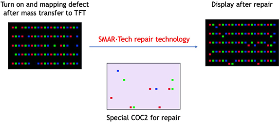
Figure 20. SMAR·Tech mass repair process with novel R/G/B chip-on-carrier step.
Download figure:
Standard image High-resolution imageThis novel R/G/B chip-on-carrier requires micro-LED chips to be arranged very precisely on the temporary carrier without local alignment key. We can make the spacing less than 2 µm by the equipment we developed. This equipment can achieve 99.9% yield of transfer process and less than 10% of current micro-LED chip cost. We did the repair process on this carrier. By replacing defect micro-LED chips by laser process, the yield on the carrier could achieve more than 99.99%.
It is unlikely to achieve ultrahigh yield after first transfer due to particles on LED wafer and backplane. Therefore, repair process is needed, and this chip-on-carrier concept also introduced to mass repair process after transferring micro-LED chips onto backplane. First, we confirmed the defect address and prepare for the repair chips with the correct arrangement. Then we could do the repair only one time. After this step, the yield could achieve to 99.9999%. If there were still some defects, we could use laser to repair each defect.
Concluding remarks
Micro-LED can be used in a variety of different application scenarios, and it provides the ultimate visual experience. The current mainstream technology to assemble a micro-LED based display is the pick-and-place technique with advanced substrate layout designs. Meanwhile, we saw an increasing demand to boost up the resolution of the display and the accuracy and precision that are involved to accomplish become a critical issue in the manufacturing process. In most cases, to transfer a large number of chips simultaneously and accurately becomes a prerequisite in this field for the next five years. Some basic practices, such as transfer printing [175], can be modified and fitted into the need for mass-production. They have to be versatile and simple to implement. A necessary understanding towards material properties, like interfacial forces and temperature variation, would be essential to master this technique. On the chip side, if the market is marching to the high resolution and high density solution, the scaling of the micro-LED chip is inevitable, and the improvement in its external luminous efficiency (cd A−1) is of paramount importance. A device with luminous efficiency higher than red 20 cd A−1, green 100 cd A−1, and blue 18 cd A−1 will suffice for most applications. This also means the chip has to give off an appropriate light output at relatively low current level. A good micro-LED should provide enough photons at the current density lower than 5 A cm−2. The major push in the next few years will be in the epitaxial quality and device design in order to achieve these goals.
In PlayNitride, we developed a novel R/G/B chip-on-carrier step to improve the transfer yield and process time. This helps the micro-LED display technology solve the challenges on transferring to non-flat surface and move to a production phase. Moving forward, hybrid solution of mass transfer should be adopted. Combination of stamp process and laser induced forward process on this novel R/G/B chip-on-carrier step could provide the production flexibility and efficiency of either large size display or high pixel density display. This will be the next topic for our mass transfer technology development.
12. Novel 2D materials for micro-LEDs
Wanqing Meng1,2, Haoliang Shen3, Bin Liu1,2 and Xinran Wang1,2,3,4
1National Laboratory of Solid State Microstructures, School of Electronic Science and Engineering and Collaborative Innovation Center of Advanced Microstructures, Nanjing University, Nanjing, People's Republic of China
2Jiangsu Provincial Key Laboratory of Advanced Photonic and Electronic Materials, Nanjing, People's Republic of China
3Suzhou Laboratory, Suzhou, People's Republic of China
4School of Integrated Circuits, Nanjing University, Suzhou, People's Republic of China
Status
Micro-LED is the ultimate display technology that could enable AR/VR experiences together with VLCs and sensing. Transferring individual LEDs to the pre-patterned backplane circuits, known as mass-transfer, is currently the most popular technique to make active-matrix micro-LED displays. This process is feasible for large pixel micro-LED displays, but not suitable for high-resolution near-eye displays due to the limitations of alignment accuracy and dense metal interconnections. Therefore, it is crucial to develop new integration processes for AR/VR applications. A promising route is the 3D heterogeneous integration of high-performance TFT backplane and micro-LED chip.
In particular, 2D materials show great potential as TFT or transparent electrode materials due to their unique properties and low-temperature back-end integration with micro-LEDs [194, 195]. Graphene, the most widely studied 2D material, has achieved remarkable progress in wafer scale growth and transfer [196], and demonstrated great potential in the GaN-based micro-LED as transparent electrodes [197]. Moreover, the epitaxy growth of GaN on sapphire suffers from a significant thermal expansion coefficient and in-plane lattice constant mismatch, which can be tackled by using graphene as the buffer layer (figure 21(a)) [198]. Other than graphene, 2D semiconductors such as MoS2 can serve as excellent TFT materials due to the following reasons. First, the monolithic fabrication of TFT on micro-LED can avoid the issues with alignment and electrical bonding in mass transfer, which improves the resolution and reduces the cost and process complexity [199]. Second, MoS2 TFT features mobility of over 100 cm2V−1s−1 and a saturation current density exceeding 1 mA μm−1, which is much superior than current TFT technologies (i.e. amorphous silicon, indium gallium zinc oxide, low-temperature poly-Si). This leads to high LED brightness at reduced power consumption. Third, the atomic thickness and flexibility of 2D materials enable new conceptual displays that are transparent and flexible [200]. To this end, Meng et al demonstrated a 3D monolithic micro-LED display at 1270 PPI driven by large-area MoS2 TFT (figures 21(b)–(d)) [181, 201]. Hwangbo et al demonstrated a direct growth of MoS2 on GaN-based epitaxial wafers, followed by patterning into TFT driving circuits [182]. These works showed the potential of 2D semiconductors to drive micro-LED displays at the ultimate resolution and brightness limit.

Figure 21. Applications of 2D materials for GaN-based micro-LED. (a), Atomic structures of GaN on atomic nitrogen irradiated graphene via the C-N-Ga-N (3) bonding structure. Insert: room temperature electroluminescence image of this N-polarity InGaN-based LED structure on GaN/Al2O3 template with atomic nitrogen irradiated graphene. [198] John Wiley & Sons. © 2020 WILEY-VCH Verlag GmbH & Co. KGaA, Weinheim. (b), Schematic illustration of the micro-LED display driven by MoS2 TFTs. Reproduced from [181], with permission from Springer Nature. (c), I–V characteristics of the individual micro-LED driven by MoS2 transistor (solid lines) and micro-LED only (red dashed line). Reproduced from [181], with permission from Springer Nature. (d), The pixel images of cartoon panda and corresponding design shown by green μ-LED display. © [2021] IEEE. Reprinted, with permission, from [201].
Download figure:
Standard image High-resolution imageCurrent and future challenges
Heterogeneous integration of 2D materials and micro-LED may revolutionize ultra-high resolution display. However, several challenges must be addressed before industrialization: high-quality 2D material growth, high-performance and scalable TFT fabrication and full-color display.
High-quality and large-area material growth is the foundation of 2D material applications. So far, only large-area graphene is available in industrial production among all the 2D materials (for example, the demonstration in Beijing Graphene Institute; www.bgi-graphene.com/). In terms of 2D semiconductors, the growth of 2-inch MoS2 single crystals [202] and 4-inch MoS2 films [203] has been demonstrated, both on GaN-compatible sapphire substrate. However, there is still a large gap between these academic research and industrial adoption, mainly in material uniformity, reproducibility, and wafer size (ideally 6–8 inches). These challenges are expected to be addressed by developing more controllable growth equipment and processes.
Other than materials quality, developing dedicated 2D material TFT processes is also critical. The challenges in 2D material TFT mainly include ultra-clean transfer from growth substrate to target substrate, Ohmic contact, dielectric integration and encapsulation. Some of the challenges already have solutions [204–207], but for TFT applications the process reproducibility and scalability, device variability and reliability remain to be examined.
Full-color displays need to have red, green, and blue subpixels. However, GaN-based red LEDs exhibit much lower QE than green and blue ones, making full-color micro-LED display a big challenge. While the industry is still seeking solutions to improve red QE through material and structural innovation, an alternative approach is to use CC by quantum dots (QDs). Existing QD patterning methods (e.g. mask-based photolithography, inkjet printing and transfer printing) still face the problems of efficiency, repeatability and accuracy, especially in high-resolution AR/VR applications. Therefore, it is pivotal to develop QDs patterning methods and CC technology that are reliable and compatible with micrometer resolution.
The development of 5G technology and the Internet of Things entails multifunctional systems that fuse display, sensing and communication. The 2D materials have been widely studied as photodetectors for their remarkable optoelectronic properties. We believe that the heterogeneous integration of 2D photodetectors with micro-LED can stimulate new conceptual devices such as biological signal detectors with displays. To this end, the hardware framework, the integration technique and the corresponding algorithms should be studied systematically, demanding multi-disciplinary cooperation among material science, physics, electrical engineering and computer science.
Advances in science and technology to meet challenges
To address the materials challenge, 4-inch wafer-scale 2D semiconductors have been grown on SiO2 and sapphire substrates, albeit with domain boundaries [208]. Single-crystal 2D semiconductors can be synthesized on Au foils by self-limited catalytic surface control, but the Au foil is expensive and incompatible with the foundry [209]. Industry-compatible and cost-effective substrates for single-crystal 2D semiconductors growth are urgently needed. Li et al reported epitaxial growth of 2-inch monolayer MoS2 single-crystal film by engineering the surface steps of sapphire (figure 22(a)). The single crystalline MoS2 has excellent wafer-scale uniformity, showing electron mobility of 102.6 cm2 V−1 s−1 [202] Wang et al found that single-crystal monolayer WS2, WSe2 and MoSe2 can also be synthesized on designed sapphire substrates. The low-cost sapphire is compatible with the foundry process and is scalable to 8 inches, which shows promise for mass production.

Figure 22. Advances in the heterogeneous integration of 2D materials and micro-LEDs. (a), 2-inch MoS2 single crystals on a C/A sapphire (0001) substrate. Reproduced from [202], with permission from Springer Nature. (b), The Au-assisted fabrication process of MoS2 transistors and the corresponding optical micrographs at each step. Reproduced from [181], with permission from Springer Nature. (c), Schematic of a 2D FET with semi-metal semiconductor contact. Reproduced from [205], with permission from Springer Nature. (d), QDs patterning process via selective electrophoretic deposition technique and the fluorescence images of multi-color QD patterns. Reproduced from [211]. CC BY 4.0.
Download figure:
Standard image High-resolution imageFor ultra-high resolution AR/VR applications, TFTs must have high driving current in limited space. The device performance highly depends on the number of scattering centers like cracks, wrinkles and impurities induced by 2D material transfer, calling for damage-free transfer techniques. Several attempts including Au-assisted transfer method (figure 22(b)) [181] and the supporting layer mechanically peelable transfer method [204] can protect 2D materials from organic solvents and residues. Nevertheless, more efforts are needed to develop polymer-, air- and solvent-free transfer techniques, ideally in vacuum. Contact resistance is another concern of semiconductor engineers due to the inherent van der Waals gap and MIGS [210]. Semi-metallic Bi contact has been reported to eliminate MIGS in MoS2 (figure 22(c)), enabling a contact resistance of 123 μm [209]. More recently, the contact resistance has been further reduced to 42 μm by enhanced band hybridization with Sb (), leading to on-state current of 1.23 mA μm−1 under 1 V drain bias [207]. This extremely high current density demonstrated the feasibility of driving micro-LEDs to the ultimate brightness and resolution limit.


Although QD printing works well for large-area displays, so far it cannot easily be extended to micro-displays due to several technical challenges. Zhao et al presented a selective electrophoretic deposition technique that patterns QDs uniformly down to 2 μm. The QDs are patterned on selective electrodes with a precisely controlled thickness (figure 22(d)) [211]. Transfer printing combined with Langmuir–Blodgett film technology is another QD patterning technique. The as-fabricated honeycomb QD patterns have an ultra-high pixel resolution of up to 25 400 PPI [212]. These strategies are expected to apply in full-color micro-LED displays driven by 2D TFTs in the near future.
Concluding remarks
In summary, the fusion of 2D materials and GaN-based micro-LEDs is a rapidly expanding field of nanotechnology. The 2D materials are not only crucial in the formation of transparent electrodes, heating dissipation layers, and epitaxy buffer layers in micro-LEDs but also have the potential to serve as robust driving components for micro-LED circuits and, in due course, as sensing units in multi-functional systems. It is worth noting that the recent advancements in 2D electronics, such as wafer-scale epitaxial growth, van der Waals contact fabrication, and high-quality dielectric deposition, have paved the way for the development of 2D TFTs technology. Researchers have successfully demonstrated prototypes of 2D TFT-driven micro-LED displays, which hold great promise for the future of display technology. Through the collaborative efforts of academia and industry, it is anticipated that within the next decade, 2D materials will achieve a significant milestone by attaining 12-inch wafer scale continuous film with high crystallinity. The advancement of 2D TFTs is expected to overcome critical technological challenges, including but not limited to ohmic contact, dielectric integration, and encapsulation, thereby leading to enhanced driving capability, uniformity, and reliability. Along with the maturation of system integration technology, it is believed that commercialized micro-LED display products will revolutionize the industry, bringing about significant contributions to the realization of the metaverse.
Acknowledgements
This work is supported by the National Key R&D Program of China (Grant Nos. 2022YFB4400100, 2021YFB3601000, 2021YFA0715600, 2021YFB3601600), the Leading-edge Technology Program of Jiangsu Natural Science Foundation (Grant No. BK20202005), the National Natural Science Foundation of China (Grant Nos. T2221003, 61927808, 61734003, 61851401, 91964202, 51861145202).
13. Semiconductor-based micro LED displays for augmented-reality applications
Kai-ling Liang, Cheng-Jhih Luo and Yen-Hsiang Fang
Industrial Technology Research Institute, Chutung, Hsinchu 310401, Taiwan
Status
AR/MR have attracted much interest due to their advanced capability of merging physical reality with digital virtuality, and they have found wide applications in gaming, entertainment, education and medical applications. In an AR device, the optical engine, which composes the main interface in the system and acts as an image projector, can generate a virtual image for our vision. The images are first emitted from the microdisplay, and then the light is coupled and guided to the eyeballs through an optical combiner. The optical engine can be a LCoS, micro-OLED, micro-LED, or LBS, whereas the optical combiners can be a reflective mirror or diffractive grating [213]. These components determine the FOV and diagonal PPD, two crucial factors that provide a better immersive experience to the users. The FOV is now mainly determined by the combiner form, while PPD alter with pixel pitch. Figure 23(a) shows the contour plot of theoretically achievable diagonal FOV at 60 PPD condition versus display size and PPI [214]. The 60 PPD corresponds to the human vision resolution limitation, and the theoretically achievable FOV can be derived from the product between PPD and FOV. Notably, it is hard to achieve high FOV and small-size displays simultaneously. The demand for higher PPI numbers is necessary; thus, the individual pixels must be smaller. Many studies have been devoted to this direction in the past two decades, as shown in figure 23(b). Full-colored OLED microdisplay has been announced since 2006 with a pitch size of 18 μm [215], and the pitch size was reduced to 6.3 μm in 2018 by Sony [216, 217]. On the other hand, semiconductor-based monochromatic displays were published in the early 2000s with a pitch of 50 μm in blue and 22 μm in green [218, 219], and were both minimized to 2.5 μm now by JBD. Traditional red micro-LED displays are more challenging due to their inherent high surface recombination. An AlGaInP-based active-matrix red micro-LED display with a pixel pitch of several tens of microns was presented in 2016 [220], and not until 2022 was a high-resolution red light micro-LED display with a pixel size of 8 μm released [221]. At the same time, red micro-LED with a single pixel size of 2 μm or less were fabricated with both AlGaInP and InGaN-based LED wafers [33, 222]. Full-color micro-LED displays were released later in 2020 with pitches of 150 μm, 24 μm and 5 μm, respectively, through various methods [114, 223, 224]. In figure 23(b), a pixel scaling trend can be fitted as ten times reduction every 17 years. These representative works as current achievements are also marked in figure 23(a) to demonstrate their optimized diagonal FOV at 60 PPD. A high-resolution microdisplay is the foundation of an AR/MR headset, and the optics and the hardware are heavily influenced by the microdisplay we adapted in the system.

Figure 23. (a) Theoretical contour plot of diagonal FOV at 60 pixel per degree (PPD) versus display size and PPI. (b) Pitch size of the full-colored OLED, full-colored micro-LED, blue light micro-LED, green light micro-LED and red-light micro-LED microdisplays.
Download figure:
Standard image High-resolution imageCurrent and future challenges
Before AR devices can be widely accepted, lightweight AR glasses with wide FOV and high PPD are required. However, the current optical design has difficulties to realize both wide FOV and compact volume together, and the PPD is limited by pixel size. The current combiners, such as the freeform optics, birdbath optics, waveguide, pin-mirrors and generic optics, all have pros and cons [109, 213, 225]. The freeform and birdbath designs provide good aberration performance but with a more extensive form and lower brightness. Diffractive waveguides are commonly used in AR due to their compactness and low cost; however, they tend to have low optical efficiency and have limitations in FOV. The FOV is governed by the refractive index of the lightguide material since the refractive index determines the total internal reflection's critical angle of the coupling light. Although several methods have been reported to increase the refractive index for broadening FOV, the refractive index of commercialized lightguide is currently available at 1.9. Additionally, the FOV, the refractive index, and the substrate's thickness further determine the maximum in-coupling grating dimensions and thus limit the combiners' etendue and the input pupil size. According to a previous report, the supporting etendue of current diffractive combiners is equivalent to a 0.34-inch display operating at f/2. To perform this display with 60 PPD retinal resolution under a 50° diagonal FOV will require a pixel pitch within 3 μm [214].
Based on the demand for fine pitch and low operating optical efficiency of waveguide systems, micro-LED displays become preferable due to their small pixel size, high brightness, and potential to reduce power consumption. JBD has released a 0.13'' semiconductor-based green micro-LED display with a pitch of 4 μm and a high brightness of over 4000 000 nits. Vuzix and TCL have integrated this micro-LED display into AR glasses and show significant performance in brightness and transparency. Vuzix presented a semiconductor-based micro-LED display AR device with a waveguide optical system in 2021 that offers a high brightness of 4100 nits and a high transparency of 90% (est). TCL also released RayNeoX2 this year with brightness over 1000 nits and transparency around 80%–95% (est). Both semiconductor-based micro-LED display AR devices show slim thickness and compact volume. Nevertheless, the micro-LED display still presents challenges when FOV and PPD need further optimization. As mentioned, while expanding the PPD, a much smaller pixel size is required. For semiconductor-based micro-LEDs, this reduction means a simultaneous decrease in EQE. Since the EQE of the device can be directly related to its power consumption, the system will suffer if the light emitters are in poor efficiency condition. The scaling in the pixels is ongoing, and the device efficiency is still sufficiently high to maintain the performance. But the situation will change once the devices' size starts approaching the one-micron regime. While the efficiency of the devices was the primary concern, the overall system performance is, however, the final match point. Besides the challenge of monochromic micro-LED, managing these small-size monochromic micro-LEDs to obtain a full-color display will be an advanced subject. As shown in figure 23(a), most works of micro-LEDs which are related to higher PPI and smaller panel sizes at the current stage are monochromatic results.
Advances in science and technology to meet challenges
To overcome these challenges (now and future), several technologies should be helpful. The FOV can be widened by the observation method or an alternative novel see-through optical module. The Maxwellian-type display can provide better vision comfort with great FOV by the eye-box enlarged techniques. NVIDIA demonstrate a projector-based Maxwellian-view display with an 85° x 78° FOV per eye [226]. Also, the Wu team exhibited AR with 100° FOV by coupling the Maxwellian view with a waveguide combiner [227]. Alternatively, a novel see-through optical module is proposed to replace the current light engine and optical combiner. Samoilova et al demonstrates a transparent optical module comprising a proprietary see-through near-eye display and proprietary micro-lens array, in which the user can view the real and virtual images simultaneously [228]. Through optical modeling using Zemax ray tracking, this module can display a macular image with 24° FOV by 5 × 5 pixel patch groups of micro-LEDs (3 x 3 of 3 μm micro-LEDs/pixel patch group). Once the pixel patch group number is enlarged, the FOV can be further increased. We also present a similar design idea with a further modification, as shown in figure 24. This see-through module includes a transparent micro-LED display, a layer of metalens and a set of optical sensor arrays which can track eye movement. The transparent micro-LED display provides high brightness and reduces the light engine volume. The meta-surface has been considered a potential solution for optical integration. Properly designing the sub-wavelength meta-atom structures on a surface reduces the volume of the optical lens. The design flexibility of the meta-surface is beneficial for polarization, aberration, and multi-function control [229]. The optical sensor-based eye trackers utilize photodiodes to gather eyeball information, which creates a slimmer design. These novel see-through optical modules present the potential of future AR to achieve wide FOV and compact volume simultaneously. Meanwhile, optical efficiency can be significantly increased since the etendue conversation is expanded with wider FOV and input pupil area, thus lowering the power consumption of the AR devices.

Figure 24. The conceptual illustration of a novel see-through optical module on the AR device.
Download figure:
Standard image High-resolution image
In parallel, the efficiency of the micro-LEDs can be significantly enhanced by using proper passivation on the sidewall to increase the brightness. Thin film technology, such as ALD, can provide a suitable dielectric material (SiO2, Al2O3, etc) to cover the sidewall and reduce non-radiative recombination. Wong et al reported an EQE boosted by 150% through Al2O3 ALD sidewall passivation of an AlGaInP red micro-LED device [12]. A rapid thermal annealing and an ammonium sulfide (NH4)2S chemical treatment can further improve the sidewall management before ALD passivation [230]. Chemical treatment of KOH followed by Al2O3 ALD and SiO2 PECVD has also been reported for an EQE increase of a small size InGaN/GaN micro-LED down to 2 μm [33]. Meanwhile, SiO2 PECVD passivation, an important passivation material in the semiconductor industry and commercially available, has been verified on small-size 2 μm AlGaInP red micro-LEDs [222]. To move forward, the production grade of thin film deposition is needed, and recently, several companies, such as Oxford Instrument®, Veeco®, and Picosun®, announces the availability of the ALD equipment for 200 to 300 mm wafers. The fabrication of miniaturized micro-LEDs can really benefit from this development in the industrial technology.
Another novel defect-free sidewall method was recently reported with epitaxy and cleanroom technologies [231]. Using selective area growth of MQW LED heterostructures on hexagonal boron nitride (h-BN) template, small-size micro-LED arrays with smooth crystalline sidewalls can be produced, and the arrays can be successfully lift-off and transferred due to comparably weak vertical van der Waal forces between LED and h-BN substrate. Besides these defect-free sidewall technologies, other novel small-sized pixelation method is also under development. Using tailored ion implantation to create a confined non-radiative region, Park et al successfully fabricated high-efficient electrically-driven pixelated InGaN micro-LEDs at the sub-micrometer scale [126]. These methods sometimes can combine with ALD coating to provide a much improved passivation for the devices. However, there are still difficulties need to be overcome. For the chemical treatment, the uniformity of the chemical etch/reaction is a great concern, and a several percent variation, which can easily cause damages of micron-sized devices, can be expected in general. The ion-implantation could be applied to a large area and is a mature technology to be worked with, and the current challenges will be the balance between electrical isolation and the luminance degradation in the ultrasmall devices [126]. The direct epitaxial growth method, which was applied in the traditional III–V based material growth, is very attractive and the recent demonstration on the ultrasmall devices is impressive. The device size defined by growth instead of etching could fundamentally reduce the sidewall recombination, but the average leakage currents demonstrated by various groups indicates more optimization is needed for the final adaptation of the technology.
Obtaining a full-color micro-LED display would be more challenging than a monochromic display since much fewer steps are involved for a single color display. People have been developing several methods to realize a full-colored microdisplay, which includes the optical combiner method, color conversion method and vertical stacking method. The optical combiner method couples emission light from separate blue, green and red micro-LED panels into full-colored images directly through a trichroic prism [232]. However, three panels and the prism enlarge the device's volume and weight. Also, the distance between the projection lens and panels reduces the FOV [109]. The color conversion method, as another full-color choice, integrates blue light micro-LED with quantum dot (QD) material to generate red and green photons. As the QD pattern size decreases, the color conversion efficiency declines due to insufficient thickness (thus optical path), resulting in blue light leakage. Hence, developing thin-film QD material with high optical density or applying a color purify layer such as DBR would be helpful [154]. In addition to these packaging integration thoughts, working on the chip itself also attracts lots of attention. The vertical stacking method assembles three colors of micro-LED vertically in the same pixel and shares the same optical aperture, and this design can greatly increase the density of the pixels. The vertical stacking micro-LED display with a pixel pitch of 5 μm was demonstrated by Ostendo Technologies Inc [224]. Similarly, researchers from Fudan University revealed a full-colored display with multi-wavelength MQWs. In such an epitaxial structure, each pixel can vary the light wavelength through the current control [233]. Both vertical stacking and multi-wavelength method can triple the resolution density and miniaturize the panel size. These advanced display technologies can greatly accelerate the transformation of monochromic micro-LED into full-colored displays.
Concluding remarks
With the rising interest for wider FOV and lighter HDMs, a higher resolution and higher PPI of full-colored microdisplays are in great demand. This article demonstrates the specification roadmap of pitch size from 2000 to 2022 and their relation with FOV at 60 PPD. The collected data from the past showed the lack of small-sized and high-resolution displays for wide-optimized FOV. The optics combiner system and the micro-LEDs must be greatly improved before we can finally realize the ultimate AR goggles. The challenges are significant, but we are also equipped with various technologies to help us reach the goal, including novel optics design in metalens and Maxwellian type system to widen the FOV, ALD to boost the EQE of the micro-LEDs, several technical methods to transform monochromic micro-LED to full-color. Together with the revolution in the materials and package methods, we hope the long-expected AR/XR world can finally arrive in the near future.
Acknowledgements
The work is supported by the Industrial Technology Research Institute (ITRI), HsinChu, Taiwan, with MOEA Contract No. 111-EC-17-A24-1579.
14. Conclusion and future perspectives
Chien-Chung Lin1, Yuh-Renn Wu1 and Hao-Chung Kuo2,3
1Graduate Institute of Photonics and Optoelectronics, National Taiwan University, Taipei 10617, Taiwan
2National Yang Ming Chiao Tung University, No. 1001, Daxue Road, East District, Hsinchu City 300093, Taiwan
3Semiconductor Research Center, Hon-Hai Research Institute, Taipei, Taiwan
A full-color, power-efficient, and cost-effective display is a much thought-after goal in the next phase of the development of display technology. In this roadmap, we collect critical viewpoints from experts worldwide and provide their forecasts for this micro-LED and its related field. We hope this information could be used as a guideline in the future.
The major driving forces of this technology are the semiconductor crystal growth and fabrication that have been in the industry for the past five or six decades. However, like its silicon counterpart, the pathway toward miniaturization is always tricky and painstaking. The epitaxial growth of the micro-LEDs with different colors, like UV and red, remains of paramount importance to the success of the field. Meanwhile, the novel epitaxy method or design, such as CSE, TJs, or nanowires, could greatly expand our view towards the scaling of the micro-LEDs due to their potential elimination of device defects. In the next 5 or 10 years, there should be considerable efforts for the active material with different bandgaps or with different structures by using the currently available semiconductor manufacturing facilities.
Meanwhile, novel materials, such as 2D materials, eutectic solders, and colloidal quantum dots, will be tested continuously to explore the unfulfilled demands of monolithic and semiconductor-based technology. A material platform for the high conductivity of transparent electrodes, integrated multi-functional sensing units, stretchable metal frames, and CC shall be ready in the next decade, where the monolithic epitaxy method might not be sufficient. Notably, the current pick and place method can be applied on a regular basis for mini-LED signage displays, and novel transfer technologies, such as electromagnetic transfer or laser transfer, will require new materials to comply with them. These new methods will lead the way to high-resolution pixel transfer.
Finally, a technology without applications or commercialization cannot sustained itself. The LED based outdoor signage has been on an uptick recently while other applications like smartwatches and AR/MR goggles are still under development. The color quality, power consumption, and resolution could be the breakthrough for the micro-LED-based display in the next few years, but the true turning point for the market acceptance would be the cost of the ownership. The broad penetration of micro-LED-based technology will eventually come true with better design, the advanced epitaxy mentioned earlier, and progress in material. This roadmap provides a stint of the micro-LED, its related technology, and a potential future direction for the next decade. We expect a broader engagement from academia and the industry, and their collaboration can foster a brighter future for micro-LEDs.
Data availability statement
The data cannot be made publicly available upon publication because they are owned by a third party and the terms of use prevent public distribution. The data that support the findings of this study are available upon reasonable request from the authors