

Abstract
This paper reviews the phase flicker associated with the phase-only liquid crystal on silicon (LCOS) technology. The phase response of the LCOS device often fluctuates with the driving waveforms. Such phase flicker can cause detrimental effect in applications operating on either holographic or non-holographic principles. The origin of the phase flicker and its impact on the performances of various LCOS-based optical systems are explained. Methods to characterise the temporal response of the LCOS device will also be presented. The efforts to reduce the phase flicker in LCOS devices were reviewed. Perspectives on the future directions are also given.
Export citation and abstract BibTeX RIS

Original content from this work may be used under the terms of the Creative Commons Attribution 4.0 license. Any further distribution of this work must maintain attribution to the author(s) and the title of the work, journal citation and DOI.
1. Introduction
Phase-only liquid crystal on silicon (LCOS) devices [1–5] are able to manipulate the optical field in a reconfigurable and efficient fashion. The technology was originally developed for information display applications including image projectors [6–9], augmented reality (AR) [10–12] and virtual reality (VR) [13, 14] displays. More recently, it has also been widely used as the optical engine in optical switches [15–20], optical tweezers [21, 22], laser pulse shaping systems [23, 24], optical coherence tomography [25], mask-less lithography [26, 27], optical microscopy [28] and 3D printing [29].
A typical LCOS device has a sandwich structure, which consists of a glass coverplate on the top, a thin liquid crystal (LC) layer in the middle and a silicon backplane at the bottom. The coverplate plate is coated with a layer of indium tin oxide (ITO) to act as the common electrode, while the silicon backplane based on the complementary metal-oxide-semiconductor (CMOS) technology has millions of individually addressable reflective electrodes, i.e. pixels. The LC molecules will respond to the voltage applied on the corresponding pixels [30]. As a result, the amplitude [31] or the phase [32] of the input optical beam can be spatially modulated, depending on the configurations of the LC. When the LC molecules are vertically aligned [33] or parallel-aligned [34, 35], the tilting angle of the LC molecule will change according to the voltage on the pixels. This leads to the change in the effective refractive index of the LC layer due to its birefringent nature. As a result, the LCOS device will only modulate the phase of the optical beam without affecting its amplitude. This type of LCOS device is often referred to as the phase-only device and has become the mainstream option in many applications, due to its high light efficiency and optical performance.
The phase response of the LCOS device needs to be stable in the systems operating on either holographic or non-holographic principles. In non-holographic systems, e.g. information display systems [7], the temporal fluctuation of the phase response, i.e. phase flicker, of the LCOS device can be filtered out by the human eyes and brains. However, the holographic systems are significantly less tolerant to the phase flicker. Holography relies on accurate representation of the phase information at any given time in order to reconstruct the intended light field. In other words, the phase information cannot be averaged with a root mean square (RMS) value. Therefore, the phase flicker of the LCOS device needs to be suppressed to an acceptable level.
In this review paper, the origin of the phase flicker in the LCOS device will be explained first. This will be followed by the impact of the phase flicker in various applications. Then, characterisation methods on the phase flicker will be presented. Efforts to reduce the phase flicker will be reviewed. In the end, perspectives on the future directions will be given.
2. Origin of the phase flicker
Figure 1 shows the generic structure of an LCOS device, which consists of a homogeneous-aligned nematic LC layer sandwiched between a glass coverplate and a piece of CMOS chip with millions of individually addressable reflective electrodes, i.e. pixels. The electrodes in LCOS devices are able to provide multiple voltage levels so that the LC molecules within the area of each electrode can be tilted into different angles. Due to the birefringence of the LC material, each pixel can exhibit various values of effective refractive indices between no and ne to a linearly polarised beam with its polarisation direction in paralleled to the LC alignment direction. The effective refractive index in this case is related to the tilting angle of the LC and the magnitude of both no and ne. Consequently, the phase delay experienced by such a linearly polarised beam, after entering the LC cell and being reflected can be controlled electrically.

Figure 1. The structure of an LCOS device.
Download figure:
Standard image High-resolution imageThe driver electronics for the LCOS device can be either analogue [36, 37] or digital [38]. In analogue LCOS devices, the pixel electrodes are driven by digital to analogue converters (DACs) and therefore are able to generate multiple voltage levels. In contrast, the pixels in the digital LCOS devices are only able to generate two voltage levels. The pulse width modulation (PWM) scheme is employed to generate multiple root mean square (RMS) voltage levels. In both types of the LCOS devices, the electrical field across the LC layer needs to be flipped on a regular basis to prevent the accumulation of ions on the electrode [39, 40]. Such accumulation of ions is undesirable because it will change the anchoring energy between the LC molecules and the alignment. As a result, the performance of the LC device will degrade over time. This DC-balanced driving scheme proves to be an effective way to improve the lifetime of the LC devices.
Both types of LCOS devices could exhibit phase flicker. However, the origin of the phase flicker can be different between them.
2.1. Analogue devices
The analogue LCOS devices are traditionally associated with higher optical performances, especially in terms of the phase flicker, when compared with the digital ones. The primary source of phase flicker in analogue LCOS devices is the field inversion process [41] that is necessary to ensure the lifetime of the LCOS device. Figure 2 illustrates two schemes to implement the field inversion in analogue LCOS devices. In the first scheme shown in figure 2(a), the voltage of the pixel electrode flips around the voltage of the ITO electrode, which remains fixed. It can be seen from figure 2(b) that the absolute electrical field across the LC layer, which the LC molecule responds to, is tuned by the voltage of the pixel electrode. While this scheme looks straightforward, it doubles the required the voltage range of the pixel electrodes. In the second scheme [42] illustrated in figure 2(c), the voltage on the ITO electrode is modulated too. Although this scheme is more complicated, the required voltage level is halved in this scheme.

Figure 2. (a) The waveforms on the pixel electrode and ITO electrode when using the first field inversion scheme; (b) the voltage drop across the LC layer in the first scheme; (c) the waveforms on the pixel electrode and ITO electrode when using the second field inversion scheme; (b) the voltage drop across the LC layer in the second scheme.
Download figure:
Standard image High-resolution imageIn both schemes, the voltage level on the ITO electrode needs to be set precisely. It can be seen from figures 2(b) and (d) that a slight offset of the ITO voltage from the target level will introduce fluctuation of voltage drop across the LC layer, which will further lead to the phase flicker. However, the pixel electrode and the common ITO electrode are made of different materials with different electrical properties. The difference in electrode work function produces a potential difference between the electrodes [33, 43]. This potential difference is sensitive to surface and interface properties and therefore often varies across the device area. As a result, it is impossible to have a universal ITO voltage setting that is ideal for all the pixel electrodes.
Each pixel electrode in the analogue LCOS devices are embedded with a storage capacitor, which will be refreshed on a regular frame basis. The storage capacitor should be able to hold the voltage level between the refreshing cycles. Due to leakage current, however, the storage capacitor will discharge slowly discharge, which will further lead to a drop in the voltage on the pixel electrode. As the LCOS devices progress towards to smaller pixel sizes, it becomes increasingly challenging to embed storage capacitors with sufficient capacitance under the pixel electrodes as the area available for each storage capacitor gets smaller. As a result, it is difficult to maintain the voltage on the pixel electrode between the refreshing cycles and phase flicker will become an issue for the analogue LCOS devices. This is one of the fundamental challenges for the analogue LCOS devices to scale towards smaller pixel sizes.
2.2. Digital devices
To overcome the complexity of the electronics for the pixel electrode in analogue LCOS devices, digital driving based on the PWM scheme is proposed for the LCOS device. Storage capacitors are no longer required for the pixel electrodes in the digital LCOS devices. In addition, the digital electronics are also simpler and faster than the analogue ones. Therefore, this type of LCOS devices has better scalability towards higher pixel resolutions and frame rate. The digital LCOS devices also promise to deliver lower power consumption and costs. However, the digital LCOS devices are traditionally associated with relatively large phase flickers, which prevents its applications in the holographic systems.
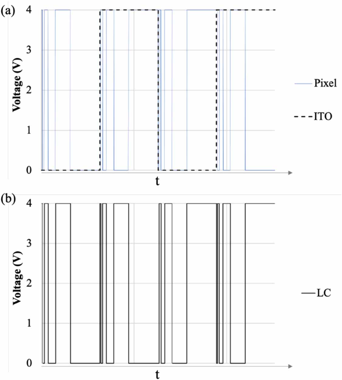
As illustrated in figure 3, the field inversion is usually realised by modulating the ITO electrode in digital LCOS devices. Similar to the analogue LCOS devices, this field inversion process will contribute to the phase flicker in the digital LCOS devices. However, the primary source of the phase flicker is the PWM driving waveforms. It can be seen from figure 3(b) that the absolute electrical field across the LC layer in the digital LCOS device is oscillating between the two possible levels. The tilting angle of LC molecule will respond to this waveform and result in the severely phase flicker. Therefore, it is traditionally believed that the digital LCOS devices are not suitable for holographic applications.
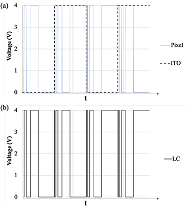
Figure 3. (a) The waveforms on the pixel electrode and ITO electrode in digital LCOS devices; (b) the corresponding voltage drop across the LC layer.
Download figure:
Standard image High-resolution image3. Impact of phase flicker
The phase flicker of the LCOS devices can affect the optical performance of the systems in different ways. Depending on the optical setup and the application requirement, some systems are more tolerant to the phase flicker than others. This section will present the impact of the phase flicker in the LCOS devices in different systems.
3.1. Non-holographic systems
The LCOS technology was originally developed for the image projectors. Figure 4 shows a typical architecture for the LCOS-based image projectors. The polarisation beam splitter (PBS) acts as crossed polarisers. The LCOS device is operating on the phase-only mode with their LC directors aligned 45° with respect to the crossed polarisers. In this case, the LCOS device act as a variable waveplates and is able to modulate the spatial amplitude of light that is projected to the screen. When the LCOS device introduces even multiples of λ/2 phase delay to the incoming beam, it will not rotate the polarisation director of the incoming beam. Therefore, the light will not be able to pass through the PBS on the return path and a dark image is delivered. When odd multiples of λ/2 phase delay is introduced to the incoming beam, its polarisation director will be rotated by 90°. As a result, a bright image is delivered.

Figure 4. A typical architecture for the image projector based on the LCOS devices.
Download figure:
Standard image High-resolution imageThe phase flicker in the LCOS device will result in the temporal variation in the brightness of the projected images as shown in figure 5. However, the human brains are able to filter out such flicker as long as its frequency is above a certain threshold [44], e.g. 60 Hz. As a result, the perceived image can have the correct brightness. Even if the flickering frequency is above 60 Hz, however, recent studies [45, 46] indicated that such systems could negatively affect human's vision. It should be noted that the image used in this test is from McGill Calibrated Colour Image Database [47].

Figure 5. Temporal variations in the brightness of the projected images and the filtering effect of human brains.
Download figure:
Standard image High-resolution imageIn addition, the phase flicker needs to be carefully managed in order to achieve high contrast ratio [48]. In order to deliver an extremely dark image, the phase response of the LCOS device needs to be fixed to even multiples of λ/2. The phase flicker in the LCOS device will cause temporal deviation from this phase level and brighten up the image. Therefore, high-end image projectors with ultra-high contrast ratio relies LCOS devices with minimal phase flicker.
3.2. Holographic systems
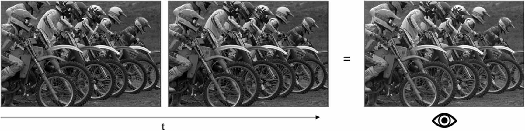
In the holographic image projection systems, the crossed polarisers are no longer required. The phase-only LCOS device modulates the wavefront of input beam and, with the help of optics, generates a 2D or 3D light field that presents the target image. For the simplicity, the analysis on the impact of the phase flicker in this section will be based on a holographic 2D image projection system. In the example given in figure 6, figure 6(a) is a phase-only hologram for the image shown in figure 6(b). This hologram was calculated by the Fienup algorithm [49] and showed decent image quality. To simulate the effect of the phase flicker, two phase-only holograms were generated and shown in figures 6(c) and (e). The phase levels in these two holograms randomly deviate from the one shown figure 6(a) on the pixel basis. However, the average between these two holograms equalled to the figure 6(a) on the pixel basis. Their corresponding relay fields were shown in figures 6(d) and (f), respectively. The perceived image shown in figure 6(g) was derived by averaging the figures 6(d) and (f). It can be seen that the image quality was severely degraded. Such noise will not be filtered out the human brains. Therefore, the phase flicker needs to minimise in the holographic image projection systems to ensure a good perceived image quality.

Figure 6. Impact of the phase flicker in holographic 2D image projection system.
Download figure:
Standard image High-resolution imageThis example shows that the phase flicker in the LCOS device will have a negative impact on the quality of the reconstructed light field in the applications operating on the holographic principles. The degradation of the reconstructed light field will further affect the key performance specifications in the respective applications, although holograms are considered relatively tolerant to the noise. In the 2D or 3D information display applications, the degraded light field results in poor image quality [50]. In the optical tweezer applications, the phase flicker can affect the accuracy and stability of the optical manoeuvre [51–53]. In the holographic optical switches, the phase flicker in the LCOS device can result in the temporal variation of the insertion loss and the elevated crosstalks [54]. The temporal variation of the insertion loss imposes a modulation on the optical signal. This will reduce the signal to noise ratio, which is undesirable. In the holographic laser processing applications, the phase flicker in the LCOS devices can have significant adverse effect on the outcome of short-pulsed and high-repetition-rate laser machining [55].
Similar to the non-holographic system, the phase flicker in the LCOS device can also result in the temporal fluctuation of intensity in the reconstructed light field [56]. The impact is more significant for the binary holograms. When the multi-level phase holograms were displayed by the LCOS device, the resulted temporal variation in the intensity is less severe. It has been demonstrated in [57] that a RMS phase flicker of 20° will only introduce <5% variation in the temporal diffraction efficiency of the blazed grating phase patterns.
In some cases, the phase flicker can also impact the performance indirectly even though it may not be the primary source of the problem. In the holographic optical switches, the crosstalk is primarily due to the fringing field effect [58, 59] of the LCOS device. Due to the elasticity of the LC material and crosstalk between the neighbouring pixel electrodes, the LCOS device is unable to display abrupt phase change properly. This is often referred to as the fringing field effect. The fringing field will distort the ideal beam-steering hologram loaded to the LCOS device and leads to elevated crosstalk levels. Iterative algorithms [60, 61] are often used to optimise the holograms to suppress the crosstalk. During the optimisation, the algorithm uses the measured performance as the system feedback at the end of each iteration. This feedback will be used to decide how to update the phase-only holograms for the next iteration. The accuracy of the feedback is often the key for such algorithms to progress effectively. In the presence of the phase flicker, the feedback signal becomes noisy and therefore less reliable. As a result, the high-quality beam steering holograms cannot be retrieved, and stringent crosstalk requirement may not be met. In the example shown in figure 7, the simulated annealing algorithm [62] was used to suppress the −1st diffraction order of a blazed grating hologram with a period of 7 pixels. The fringing field effect was simulated by a Gaussian filter function on the grating profile. The effect of the phase flickering was simulated by introducing <±0.5 dB uncertainty to the power of the −1st diffraction order. It can be seen that the phase flicker increased the crosstalk by ∼8 dB in this specific case.
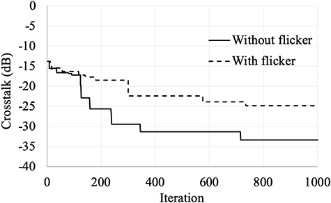
Figure 7. The progression of the simulated annealing algorithm for crosstalk suppression with and without the influence from the phase flicker.
Download figure:
Standard image High-resolution image4. Characterisation of the phase flicker
The phase response of the phase-only LCOS devices cannot be measured directly. With the help of optical systems, the phase response of the LCOS device can be translated into the change in the intensity. Therefore, the phase response can be derived from the intensity change. This section will describe the most common principles for the characterisation of the phase response and flicker of the LCOS devices. It should be noted that these methods are only suitable for the phase-only LCOS devices, in which the LC molecules are either parallel-aligned or vertically aligned. They should not be used to characterise the responses of LCOS devices with different LC configurations, e.g. twisted nematic LCOS devices.
4.1. Polarimetric system
Figure 8(a) shows the optical setup of LCOS characterisation system based on the polarimetric principle [63, 64]. This is one of the most widely used setup for the LCOS characterisation. In this setup, the LCOS device was placed in between a pair of crossed polarisers, i.e. P1 and P2. The polarisation director of the LCOS device was aligned 45° with respect to each polariser. Similar to the non-holographic projector system shown in figure 4, the change in the phase response of the LCOS device will be translated into the intensity change at the detector when a laser is used as the light source. The relationship between the total phase delay introduced by the LCOS device and the intensity at the detector can be described as:


where I is the detected intensity; Io is the intensity of the input light;  is the phase delay introduced by the liquid crystal layer; neff is the effective refractive index of the liquid crystal molecule, which is dependent on its tilting angle; d is the thickness of the LC layer;
  is the wavelength of the input light. By measuring the intensity at each grey level, the corresponding phase response of the LCOS device can be derived based on equation (1). Figure 8(b) shows a typical measured relationship between the grey level and the intensity at the detector. It should be noted that the intensity level at Grey Level 0 depends on the LC property and the thickness of the LC layer. When a high-speed photo detector is used, the temporal variation in the intensity as shown in figure 8(c) can be converted into the phase flicker of the LCOS device under the test as shown in figure 8(d).
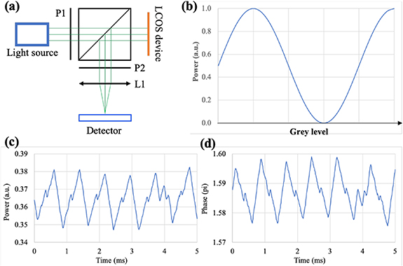
Figure 8. (a) the optical setup of the polarimetric system for phase characterisation of the LCOS device; (b) a typical measurement result; (c) an example of the temporal response measured by the high-speed photo detector; (d) the calculated phase flicker.
Download figure:
Standard image High-resolution imageIn addition to its simplicity, one of the key advantages of this setup is its ability to characterise the phase response on the pixel basis. When a high-speed camera is used as the detector and a microscopic lens is used as L1, the phase flicker of each pixel can be measured by the camera. This is useful when the pixels flicker in an asynchronised way. Figure 9 shows an example of the spatial phase flicker of an LCOS device measured by such system. In this specific example, a hologram with two different grey levels are loaded to the LCOS device. The high-speed camera captures the spatial and temporal response of the LCOS device at a rate of 600 frame per second. It can be seen that pixels with the same grey levels are not flickering in a synchronised manner. This behaviour normally happens in the digital LCOS devices, where the driving waveforms for the pixels at the same grey level are not necessarily in phase.

Figure 9. The spatial phase flicker measured by the crossed polarisation microscopic system with a high-speed camera.
Download figure:
Standard image High-resolution imageIt should be noted that there will be uncertainties in deriving the phase response and flicker around the turning point of the measured intensity curve. In some cases, this will make the calculated phase flicker artificially high. This is because a small power fluctuation can be translated into a relative larger phase variation in those circumstances. As a result, the noise from the high-speed photodetectors would play a significant role.
In order to address this issue, Martínez et al [65, 66] proposed an extended linear polarimeter for the phase characterisation as shown in figure 10. In this setup, two detectors are used. The linear polariser placed in front of each detector was aligned at the different angles with each other. An analytical model was built to derive the actual phase flicker around the turning points of the measured curves. This approach also made it possible to analyse the de-polarisation effect of the LCOS device.
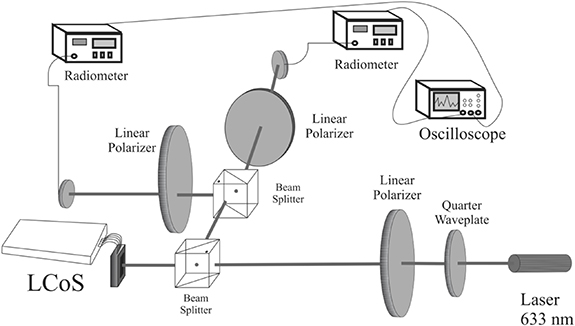
Figure 10. The extended linear polarimetric systems for the phase response and flicker characterisation. Image courtesy of [66].
Download figure:
Standard image High-resolution image4.2. Diffractive system
The static and temporal phase response of the LCOS device can also be measured by using a diffractive optical system [67, 68]. In the example shown in figure 11(a), the input laser beam and the LCOS device are placed at the front and back focal plane of the collimating lens (L1), respectively. A series of binary grating phase patterns (as shown in figure 11(b)) with a fixed period of T but variable peak-to-valley phase depth (Δ(t)) are loaded into the LCOS device. The corresponding power of +1st or −1st diffraction order is measured. The relationship between the peak-to-valley phase depth and the power of ±1st diffraction order can be described by equation (3).

where Po equals the maximum power possible for the ±1st diffraction orders. This relationship was also plotted in figure 11(c). A high-speed photo detector can be placed at the position of either the +1st or −1st diffraction order to measure the average power and the temporal power fluctuation. The measured results can be converted back into the average and temporal phase response of the LCOS device.
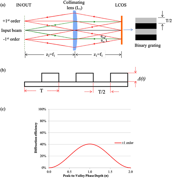
Figure 11. (a) a diffractive optical system for measuring the phase flickers in the LCOS device; (b) the cross-section of the binary grating; (c) the power response of the ±1st diffraction order to the peak-to-valley phase depth in the binary grating. Image courtesy of [69].
Download figure:
Standard image High-resolution imageSimilar to the standard polarimetric system, there will be uncertainties in deriving the phase response and flicker around the turning point of the measured intensity curve in the diffractive system.
Unlike the polarimetric system, the photo detector in this system will not receive any signal when the voltage is not applied to the LC. This makes the data processing more straightforward. However, it should also be noted that the measurement results could be unreliable if the pixels with the same grey level flicker in an asynchronised way.
4.3. Interferometric system
The phase response of the LCOS device can also be measured by the interferometric system. In [70], Twyman-Green interferometer (as shown in figure 12(a)) was used to measure the temporal phase fluctuation of the LCOS device under the test. As shown in figure 12(b), the light reflected from the LCOS device and the reference mirror will form interference patterns at the camera plane. By analysing the captured interference pattern, the phase response of the LCOS device can be derived. The temporal fluctuation in the phase response of the LCOS device will lead to temporal shift in the interference pattern. This can be used to calculate the phase flicker in the LCOS device. A typical phase flicker result is presented in figure 12(c). When properly designed, this system is also able to analyse the phase flicker of the LCOS device on the pixel basis. When compared with the two setups described in the above, however, it is more complicated to set up the interferometric system. It also requires high-speed camera and sophisticated image processing algorithm to derive the phase response and flicker of the LCOS device with high accuracy.
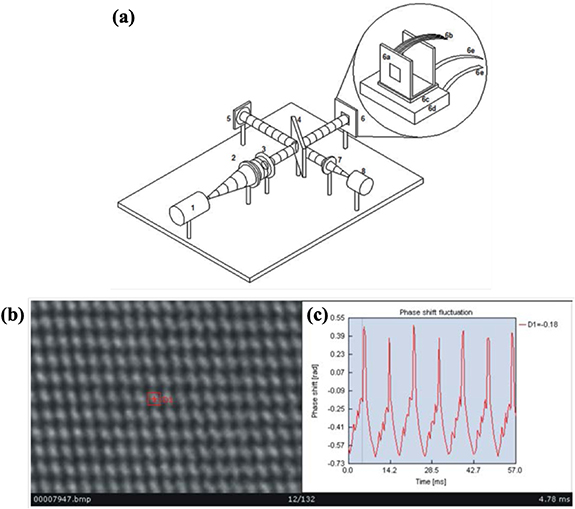
Figure 12. (a) Twyman-Green interferometer used to measure the temporal-phase fluctuations, (1) He-Ne laser, (2) collimator, (3) pupil, (4) beam splitter, (5) flat mirror, (6) LCOS-SLM and temperature controller, (7) focusing lens, (8) high-speed CCD; (b) the interference pattern captured by the camera; and (c) derived phase fluctuation. . Image courtesy of [70].
Download figure:
Standard image High-resolution image5. Phase flicker minimisation
In this section, various methods to suppress the phase flicker in the LCOS devices will be presented. Their pros and cons will also be discussed.
5.1. High-frequency field inversion
The phase flicker in the analogue LCOS devices can be effectively suppressed by increasing the frequency of field inversion. In the early versions of the LCOS backplanes, the field is inverted on the frame basis, as shown in figures 13(a) and (b). Recently, the field inversion frequency is decoupled from the frame rate as illustrated in figures 13(c) and (d). Although the amplitude of the temporal fluctuation in the electrical field across the LC layer will not be reduced by the increased field inversion frequency, it shortens the duration that the LC molecules can tilt towards either directions. This can be effective in minimising the phase flicker. With increased field inversion frequency, the capacitor embedded under each pixel electrode will also be refreshed more frequently. This will limit the voltage drop due to the current leakage between the refresh cycles and therefore further reduce the phase flicker.

Figure 13. (a) and (b) standard analogue driving waveforms; (c) and (d) the corresponding high-frequency analogue driving waveforms.
Download figure:
Standard image High-resolution imageState-of-art analogue LCOS devices implement the field inversion by modulating the voltage on the ITO electrode, as most of the digital LCOS devices do. The modulation frequency for the ITO electrode can be as high as several kilohertz [71, 72]. This is much faster than the response speed of most nematic LC materials. Therefore, the residual high-frequency variation in the electrical field across the LC layer will not be translated into the phase flicker. This proves to be the most effective and practical way to minimise the phase flicker in the analogue LCOS devices. As the field inversion rate is different to the frame rate, this driving scheme requires more complicated circuit structure for the pixel electrodes[42].
5.2. DC-balancing
As explained in the first section of this paper, the voltage on the ITO electrode needs to be fine-tuned to minimise the temporal variation in the absolute electrical field across the LC layer and therefore the phase flicker. This will also help to prolong the lifetime of the LCOS device. However, the correct ITO voltage setting can be area dependent because the potential difference between the pixel electrode and ITO electrode are sensitive to the interface properties between the electrodes and the LC material. Therefore, it is impossible to optimise the ITO voltage across the whole device area. Nevertheless, the ITO voltage needs to be set correctly at least for some part of the LCOS device in order to the suppress the phase flicker as much as possible.
This method is most useful for analogue LCOS devices with low-frequency drivers. In the state-of-art analogue devices and most digital devices, the high-frequency field inversion minimises the impact of non-ideal ITO voltage on the phase flicker. The fine-tuning of the ITO voltage can only lead to marginal improvement on the temporal stability of the LCOS device.
5.3. Temperature tuning
Phase flicker can also be suppressed by lowering the operation temperature [70, 73, 74] of the LCOS devices. This method is applicable to both analogue and digital LCOS devices. The LC material becomes more viscous at lower temperature. Therefore, it will respond to the change in the electrical field more slowly [75]. When the electrical field fluctuates significantly faster than the response of the LC material, its temporal variation is effectively filtered out by the LC. As a result, the LCOS device will not exhibit significant phase flicker. As shown in figure 14 [70], the phase flicker has been reduced by at least one order of magnitude when the LCOS device was cooled from 25 °C to −8 °C.
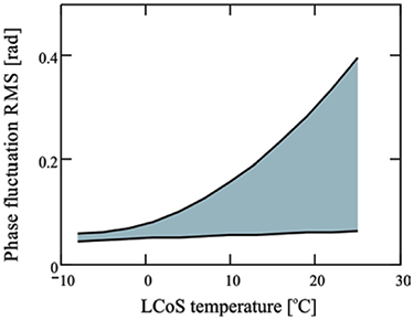
Figure 14. The relationship between the phase flicker of the LCOS device and its operating temperature. Image courtesy of [70].
Download figure:
Standard image High-resolution imageIt should be noted that this method is not suitable for every application. The reduced operation temperature of the LCOS device also leads to increased respond time [75] of the LCOS device. This could be an issue for the systems that require fast response. For example, the image projection system requires a framerate of at least 60 Hz. It is difficult for LCOS device to achieve this when it is operating at 0 °C. This method is not suitable for optical switches based on the LCOS technology either. The operation temperature of the LCOS device in these applications is usually raised to 50 °C or even higher so that the optical switches can pass the Telcordia qualification and be deployed in the harsh environment. It should also be noted that cooling the LCOS device to sub 10 °C also requires significant energy. This may not be acceptable in many applications where the power consumption is the key.
5.4. LC material
It can be seen from the discussion in sections 5.3 that the viscosity of the LC materials can have a significant impact on the level of the phase flicker in LCOS devices. By using the LC material with high viscosity, the phase flicker in the LCOS device can be reduced. However, this will also lead to slow response and elevated fringing field effect, which are undesirable in many applications.
5.5. LC cell thickness
The phase flicker in the LCOS device can also be reduced by increasing the thickness of the LC layer. The mechanism of this method is similar to that of operating the LCOS device at lower temperature. The response of the LCOS device becomes slower as the thickness of the LC layer increases [76]. As a rule of thumb, the response time of the LCOS device would quadruple if the thickness is doubled. As a result, the temporal fluctuation of the electrical field will result in less phase flicker. Compared with the temperature tuning, this method requires significantly less energy as the power-hungry cooling system is no longer required.
However, this method is still not suitable for applications where the response time is critical for the obvious reasons. In some of the wavelength selective switches (WSSs) [77], LCOS devices with a total phase depth of > 3.5π instead of > 2π [78] is used to address the phase flicker. This is possible because WSSs can allow a response time of ∼1 s in many scenarios. But the increased cell thickness also leads to significantly stronger fringing field effect, which can distort the phase hologram loaded to the LCOS device. The most pronounced side effect is elevated level of higher diffraction orders, which is particularly undesirable for LCOS-based optical switches, e.g. WSSs. Advanced hologram optimisation schemes [79] need to be used to suppress the higher orders and meet the stringent crosstalk requirement.
5.6. PWM optimisation
Recent effort on the phase flicker suppression focuses on the optimisation of the PWM driving sequences for the digital LCOS devices. In the analogue LCOS devices, only the DC balancing could be fine-tuned once the silicon backplane and the driving electronics have been designed. In contrast, the digital LCOS devices give operators more freedom in the optimisation of the driving waveforms. The change the pulse width and the sequence of the pulses can result in significantly different temporal phase responses. State-of-art digital LCOS devices can support tens of billions of the possible driving waveforms. This also makes the optimisation process challenging as it is impossible to experimentally verify each waveform.
In order to address these issues, our previous work [69] experimentally evaluated the LC's response to ON or OFF pulses width different durations as shown in figure 15. The experimental results were used to analyse the rise and decay characteristics of the LC molecules to different pulses. The findings were further used to construct an empirical model that was able to predict LC's temporal phase response to any PWM driving waveforms. As shown in figure 16, a decent match between the predicted and experimentally measured responses were achieved.
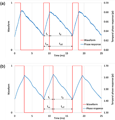
Figure 15. (a) and (b) LC's temporal phase responses to ON or OFF pulses with different duration. Image courtesy of [69].
Download figure:
Standard image High-resolution image
Figure 16. The comparison between the predicted and measured temporal phase response to a PWM driving waveform. Image courtesy of [69].
Download figure:
Standard image High-resolution imageSubsequently, this empirical model was used to select the PWM driving waveforms with minimum phase flicker from a subset of the possible pulse combinations without the need for further experimental works. This significantly improves the speed of optimisation. In the end, 256 PWM driving waveforms were generated to realise phase modulation between 0 and 2π. As shown in figure 17, the peak-to-peak phase flicker was reduced from ∼0.15π to 0.03π.
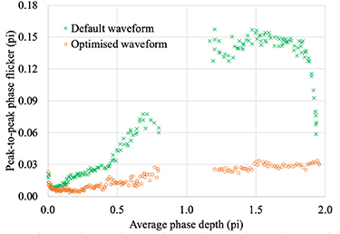
Figure 17. The phase flicker comparison between the default PWM waveforms and the optimised waveforms at different phase depths. Image courtesy of [69].
Download figure:
Standard image High-resolution imageIn another recent work [50], the PWM driving waveforms were further optimised for lower phase flicker as well as better phase linearity. It can be seen from figure 18 that the optimised driving waveforms were able to realise 256 linearly spaced phase levels between 0 and 2π. The RMS phase flicker is further reduced to ∼0.003π.
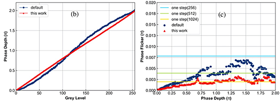
Figure 18. The phase response and flicker of the digital LCOS device under test. Image courtesy of [50].
Download figure:
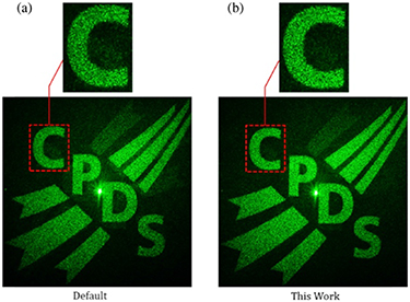
Standard image High-resolution imageIt was also demonstrated in this work that the reduction of the phase flicker in the LCOS device can result in the improvement in the image quality in the holographic image projections due to the precise display of the LCOS device. As shown in figure 19, the brightness and the uniformity of the reconstructed image has been noticeably improved by the optimised PWM driving waveforms with better linearity and lower phase flicker.
Figure 19. The phase response and flicker of the digital LCOS device under test. Image courtesy of [50].
Download figure:
Standard image High-resolution image
Both works mentioned in the above were carried out on 2 k LCOS devices for 1550 nm. Recently, Yang et al [80] also characterised the phase flicker in a 4 k LCOS device for 633 nm. The standard deviation values of the temporal phase response of the tested device was measured to be ∼0.02π. However, this value should not be compared with the work done on the 2 k LCOS devices due to the significant difference in the cell thickness. As explained in the previous section that thinner LCOS devices respond to the change in the electrical field much faster and therefore tend to have larger phase flicker.
A comparison between different phase flicker minimisation methods is given in table 1.
Table 1. Comparison between different methods for phase flicker minimisation.
| Method | Applicable devices | Advantages | Disadvantages | |
|---|---|---|---|---|
| High-frequency field inversion | Analog & Digital LCOS devices | Most effective | Requires complicated LCOS backplane design | |
| DC balancing | Useful for legacy LCOS backplanes | Challenging to implement for the whole device area | ||
| Temperature tuning | Simple to implement | Slow response Large fringing field effect | High power consumption | |
| LC material | ||||
| LC cell thickness | ||||
| PWM optimisation | Digital only | Effective for digital LCOS devices Reprogrammable | Time-consuming optimisation process | |
6. Future perspectives
Recently, the development of the LCOS devices was boosted by the emerging AR and VR applications. The key requirement for the LCOS devices in such systems is higher frame rate and pixel density. This will be the future direction for the next-generation LCOS devices and therefore stimulate the development of high-frequency driving electronics [81, 82]. It can be envisioned that those fast drivers can help further reduce the phase flicker in the LCOS devices, particularly analogue LCOS devices due to the reason explained in section 5.1. However, faster LCOS devices also rely on LC materials [83] with fast response. These LC materials would be more sensitive to the fluctuation of the electrical field across the LC layer, leading to high phase flicker. Therefore, the balance between the response time and phase flicker need to be carefully considered in the development of LC materials and driving electronics.
The pixel size of the LCOS device needs to be further reduced in order to realise LCOS devices with 4 k or 8 k resolutions [80] in a cost-effective manner. For the analogue LCOS devices, this means that the area available for the capacitor embedded under each pixel becomes increasingly smaller. Without further innovations in the capacitor structure and material, the capacitor may not be able to hold voltage level between the refreshing cycles due to the leakage current. As a result, the fluctuated electrical field across the LC layer will inevitably lead to phase flicker.
The phase flicker in the digital LCOS devices still needs further reduction, especially when operating at elevated temperatures. The works presented in section 5.5 only tested a small subset of the tens of billions of waveforms made possible by the state-of-art digital LCOS devices. As a result, it is believed that there is still huge potential for further reduction in the phase flicker of the digital LCOS devices. However, this also requires more efficient and intelligent methods to test and identify PWM driving waveforms with minimum phase flicker.
The phase retrieving algorithms can also be further developed for the holographic system based on the LCOS device to minimise the impact of phase flicker. Most of the phase retrieving algorithms were developed without consideration of phase flicker. However, the phase flicker does not only affect the performance of the retrieved phase hologram but also affect the effective progression of the algorithms. Therefore, phase flicker needs to be incorporated into the phase retrieving algorithms.