

Abstract
Semi-transparent solar cells are the next step for photovoltaics into our daily life. Over the last years, kesterite-type material has attracted a special attention to be used as an absorber in thin-film solar cells because of its low toxicity and earth abundant constituents. Here, Cu2ZnGeSe4 (CZGSe) thin films are grown by co-evaporation and subsequent annealing at a maximum temperature of 480 °C or 525 °C onto Mo/V2O5/FTO/glass stacks. The goal of this work is to investigate the influence of the annealing temperature on the composition, morphology, vibrational properties, and transmittance of CZGSe layers, the formation of secondary phases, and distribution of elements within the absorber layer as well as on the optoelectronic properties of the corresponding solar cell devices. Raising the annealing temperature to 525 °C leads to a more uniform distribution of Cu, Zn, Ge and Se throughout the absorber layer, a reduction of the presence of the GeSe2 secondary phase, which is mainly detected at 480 °C, a larger grain size and the formation of a thicker MoSe2 layer at the CZGSe/back contact interface. The strategy of increasing the annealing temperature allows for improved J–V characteristics and higher spectral response resulting in an enhanced device performance of 5.3% compared to 4.2% when using 525 °C and 480 °C, respectively. Both absorber layers present an optical band gap energy of 1.47 eV. Furthermore, higher annealing temperature has beneficial effect to the CZGSe-based devices without losses in total transmitted light because of the higher diffuse transmittance. This work shows first promising semi-transparent CZGSe-based solar cells possibly open up new routes of applications.
Export citation and abstract BibTeX RIS

Original content from this work may be used under the terms of the Creative Commons Attribution 4.0 license. Any further distribution of this work must maintain attribution to the author(s) and the title of the work, journal citation and DOI.
1. Introduction
Kesterite-type material Cu2ZnSn(S,Se)4 (CZTSSe) has gained interest to be used as absorber for thin-film solar cells in the last years. This material has the advantage of consisting of elements of low toxicity and high abundancy in the Earth's crust, having a high absorption coefficient, and a tunable band gap energy Eg between 1.0 eV (Cu2ZnSnSe4) and 1.6 eV (Cu2ZnSnS4). Efficiencies of 12.5% and 12.7% have been achieved for Cu2ZnSnSe4 (CZTSe) [1] and CZTSSe [2, 3], respectively. However, these are still very low compared to other materials used in thin film photovoltaic devices, as e.g. Cu(In,Ga)Se2 and CdTe [4]. The main limitation of the kesterite technology is its rather high VOC deficit (Eg/q− VOC) [5]. The formation of a deep Sn-related defect has been postulated as one of the reasons of the high VOC deficit of these solar cells [6–8]. The partial substitution of Sn by Ge increases the band gap energy of the Cu2ZnSn1−x Gex Se4 (CZTGSe) [9], leading to an enhanced VOC and increase in device performance for low concentrations of Ge (x around 0.22) [10]. However, the increase in the Ge content led to a decreased efficiency due to higher VOC deficit [10]. Recently, Choubrac et al [11] have shown the full potential of the total substitution of Sn by Ge in kesterite-based photovoltaic devices, achieving an efficiency of 8.5% and VOC values reaching 65% of the theoretical limit for Cu2ZnGeSe4 (CZGSe) solar cells. To achieve such high VOC, different strategies were implemented, i.e. chemical etching of the surface of the absorber layer and a heat treatment of the final device. Previously, an efficiency of 7.6% was achieved by the optimization of the CdS buffer layer to enhance the buffer/CZGSe interface [12]. Benhaddou et al [13] have shown the importance of the annealing conditions and surface treatments on CZGSe grown by selenization of sputtered metallic precursors improving the suppression of secondary phases formation and crystalline quality, obtaining a maximum efficiency of 5.6% [13], and later of 6.5% [14].
Very recently, Khelifi et al [15] have investigated the possible use of CZGSe-based devices as top cell in a tandem solar cell. They determined that the optimal Eg of the kesterite-based top cell for a four-terminal tandem device with crystalline Si as a bottom cell would be in the range of 1.5–1.7 eV. Furthermore, CZGSe-based top cells with Eg around 1.45 eV to 1.55 eV would be well suited together with CISe bottom cells with Eg of 1.0 eV [16] posing to be an option for S-free tandems, reducing the chalcogen-need to only Se in a potential chalcogenide thin-film tandem device. For that purpose, it is important to increase the transparency of the top cell maintaining a high performance. Additionally, semi-transparent kesterite solar cells start to attract the attention of the community, not only to be used for a cost-efficient tandem device, but also for bifacial solar cells and advanced building integrated photovoltaic (BIPV) concepts, further increasing their range of applications. Espindola-Rodriguez et al [17] reported bifacial CZTSSe solar cells with an efficiency of 7.7% and Eg = 1.09 eV using FTO as back contact and a Mo nanolayer between the kesterite and FTO. Later, the use of a transition metal oxides, such as TiO2 and V2O5 together with a Mo:Na nanolayer improved the back interface of CZTSe, CZTS and CZTSSe solar cells deposited on FTO, obtaining efficiencies of 6.1%, 6.2%, and 7.9%, respectively [18]. Following this idea, we recently prepared CZTGSe thin films by co-evaporation onto Mo/V2O5/FTO/glass and subsequently annealed in Se-atmosphere, achieving a device performance of 5.6%, Eg = 1.28 eV and a transmittance of 30% in the near-infrared range [19]. Other groups also investigated semi-transparent kesterite solar cells grown on ITO. However, in the latter devices, in-diffusion towards the CZTSSe absorber layer and the formation of SnOx seem to limit the conversion efficiency [20].
In this work, we propose to combine wide band gap CZGSe thin films and transparent FTO substrates. CZGSe thin films are deposited by co-evaporation onto Mo/V2O5/FTO/glass back contact structures followed by a thermal annealing treatment. We investigated the influence of the annealing temperature of the absorber layer on its transparency, structural, morphological, vibrational and compositional properties, as well as on the properties of the completed solar cells. To the best of our knowledge, a record efficiency of 5.3% (active area: 5.8%) for a 1.47 eV band gap CZGSe-based solar cells grown on FTO substrates is achieved.
2. Experimental section
2.1. Deposition of Cu2ZnGeSe4 thin films and device fabrication
Cu2ZnGeSe4 (CZGSe) thin films were deposited onto Mo/V2O5/FTO/glass by co-evaporation of Cu, Ge, ZnSe and Se at a nominal substrate temperature of 150 °C. The substrate was rotated during deposition to improve the film uniformity. Commercially available FTO (Sigma Aldrich) with a sheet resistance of 7 Ω sq−1 and an optical transmission of 80%–82% in the visible range was used. As reported in [19], a Mo (12 nm)/V2O5 (15 nm)/FTO/glass substrate structure was used to reduce the series resistance that could result in inefficient semi-transparent solar cells. The V2O5 layer was grown by thermal evaporation (Oerlikon Univex 250) using a W boat, a deposition rate of 0.5 Å s−1 and a base pressure of 4 × 10⁻⁵ mbar. The Mo-layer was deposited by DC-magnetron sputtering (Alliance Concept CT100) using 4.2 W cm−2 power density, at 1.3 × 10⁻³ mbar and at room temperature.
Because of the well-known beneficial effect of Na on kesterite-based devices [21], and the fact that FTO blocks the Na diffusion from the glass into the absorber layer [22], a 6 nm thick NaF layer was evaporated just before the co-evaporation of CZGSe thin films in the same vacuum chamber.
The co-evaporation process consisted of three stages. First, all four elements were co-evaporated simultaneously. In order to achieve a Cu-poor composition, subsequently only Ge, ZnSe, and Se were co-evaporated. Finally, only Ge and Se were evaporated for 2 min to avoid the presence of ZnSe phases at the surface of the absorber layer. A similar procedure was used to deposit Cu2ZnSnSe4, as reported previously in [23]. The used low substrate temperature was chosen to minimize the loss of Ge. A Se capping layer of around 500 nm was evaporated at room temperature in the same vacuum chamber to homogenize the kesterite surface and protect it against possible oxidation [19]. The base pressure in the vacuum chamber was of 10−7 mbar, while the working pressure was in the range of 10−6 mbar. As-grown CZGSe thin films were treated by two different thermal annealing processes in Ar atmosphere. In the first thermal process, the samples were annealed at 330 °C for 45 min at a pressure of around 4 × 10⁻¹ mbar and at 480 °C for 15 min at 900 mbar. A second annealing process was carried out, at 330 °C for 45 min at 4 × 10⁻¹ mbar, at 480 °C for 15 min at 900 mbar and at 525 °C for an additional 15 min at 920 mbar. The annealing process was performed in presence of 22 mg of pure elemental selenium (99.999%) and of 5 mg of GeSe2 placed in a partially closed graphite box and inserted into a quartz tube furnace. The heating rate was set to 20 °C min−1 and the cooling rate to 10 °C min−1.
Solar cells devices were fabricated by using a CdS buffer layer of around 50 nm deposited by chemical bath deposition followed by 50 nm i-ZnO and 350 nm of In2O3:SnO2 (ITO) layers deposited by DC-pulsed sputtering to act as a transparent conductive window layer. Before the CdS deposition, the absorber surface was etched with 2 wt % KCN for 1 min. The devices had neither grids nor antireflection coating layer. Moreover, no thermal treatment was carried out after finishing the solar cell devices.
2.2. Characterization techniques
The chemical composition was measured by energy dispersive x-ray spectroscopy (EDX) (Oxford instruments, model INCAx-sight) inside a Hitachi S-3000N scanning electron microscope (SEM). EDX measurements were carried out at 10 and 25 kV operating voltage, and the Cu K, Zn K, Ge K and Se K lines were used for quantification. Glow discharge optical emission spectrometry (GD-OES) was used to measure the in-depth element distribution through the CZGSe thin-film. The measurements were performed in a Spectruma GDA 650 spectrometer with argon plasma in a pulsed RF mode for sputtering and a CCD-array for the optical detection. The GD-OES measurements are shown in arbitrary units since they were performed without a calibration sample [24]. Grazing incidence x-ray diffraction (GIXRD) was performed to investigate the structural properties of the CZTGSe thin films. GIXRD data were collected with a PANAlytical X´Pert Pro MPD diffractometer, using CuKα radiation and a multilayer mirror to produce a parallel beam. Detector scans with incident angles of 1° and 4° were carried out. The morphology of the CZGSe/Mo/V2O5/FTO/glass structure was investigated by SEM using a SEM FEI VERIOS 460, operating at 2 kV. Raman scattering measurements of the CZGSe solar cells were performed using FHR640 and iHR320 monochromators from Horiba Jobin-Yvon, both coupled with CCD cameras. The measurements were performed in a backscattering configuration through the probe designed at IREC using gas (442 nm) and solid state (532 and 785 nm) lasers as excitation source. The laser power density did not exceed 150 W cm−2. The spectral position was calibrated by imposing the main peak of monocrystalline Si to 520 cm−1. Transmittance of the CZGSe/Mo/V2O5/FTO/glass structure was measured with a Cary Varian 5000 spectrophotometer in a range from 300 to 1200 nm. The diffuse transmittance was measured using the integrating sphere implemented in the diffuse reflectance accessory DRA-2500.
I–V characteristics were measured using a Sun 3000 class solar simulator (Abet Technologies Inc., Milford, CT, USA). Measurements were carried out at 25 °C and under air mass AM1.5 and 100 mW cm−2 illumination. External quantum efficiency (EQE) measurements were performed using a Bentham PVE300 system (Bentham Instruments Ltd, Berkshire, UK) calibrated with a Si and Ge photodiode. Internal quantum efficiency (IQE) was determined from EQE and reflectance measurement of the solar cells. Reversed voltage-biased EQE curves were collected by connecting a Keithley 2400 source meter (Keithley Instruments Inc., Cleveland, OH, USA) directly to the primary coil of the transformer and biasing the device at the desired voltage.
3. Results and discussion
Table 1 summarizes the composition of CZGSe thin films after the two different thermal treatments. The increase of maximum annealing temperature up to 525 °C has an important impact on the composition of the CZGSe layers. The increase of temperature influences the [Cu]/([Zn] + [Ge]) and [Zn]/[Ge] atomic ratios significatively. The sample annealed at 480 °C presents a Zn-poor and Cu-poor composition, which is more pronounced at the surface region of the absorber layer. However, the samples heated at 525 °C are characterized by a Cu-poor and Zn-rich composition, optimal conditions to achieve high-efficient kesterite solar cells [25].
Table 1. Composition of CZGSe thin films measured by EDX after the two different annealing processes.
| Sample | kV | Cu (at. %) | Zn (at. %) | Ge (at. %) | Se (at. %) | [Cu]/([Zn] + [Ge]) | [Zn]/[Ge] | [Se]/[M] |
|---|---|---|---|---|---|---|---|---|
| 480 °C | 25 10 | 17.2 15.3 | 12.5 9.9 | 13.7 16.3 | 56.6 58.5 | 0.66 0.59 | 0.91 0.60 | 1.31 1.41 |
| 525 °C | 25 10 | 19.1 21.8 | 13.5 12.1 | 11.9 11.6 | 55.5 54.5 | 0.75 0.91 | 1.14 1.05 | 1.25 1.20 |
Note: M = Cu + Zn + Ge.
In order to evaluate the effect of the maximum temperature on the diffusion of the elements through the absorber layer, GD-OES depth profiles were measured (see figure 1). A significant impact of the annealing temperature on the distribution of elements throughout the CZGSe/back contact structure becomes apparent as well. CZGSe annealed at 480 °C presents a very inhomogeneous distribution of all the elements, while the absorber heated at 525 °C is characterized by a very uniform distribution of Cu, Zn, Ge and Se. The sample annealed at the lowest temperature presents a significant drop of Cu and Zn and an increase of Ge, Se and Na signals in a region near the surface. The Na depth-profiles of both samples are characterized by a higher Na concentration near the back contact and the surface of the absorbers, following a U-shape, with the exception of a slightly higher Na content near the region where a significant drop of Cu signal is observed in the absorber treated at lower temperature. This effect is in agreement with the affinity of Na for Cu vacancies, VCu, which is widely observed before in CIGSe solar cells [26]. In addition, the surface of the sample annealed at 480 °C is characterized by increased Se and Ge contents and decreased Zn and Cu signals. The Sn-signal in the GD-OES-profiles comes from the FTO back contact.
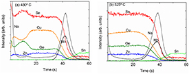
Figure 1. GD-OES depth profiles of the elements through the CZGSe/Mo/V2O5/FTO structure.
Download figure:
Standard image High-resolution imageFigure 2 shows the GIXRD patterns of both CZGSe samples. For comparison, a diffraction pattern of FTO is also plotted in figure 2(a). As it can be observed in figure 2(a), CZGSe (00-052-0867) is the main phase formed together with FTO corresponding to the back contact. In addition, the presence of a MoSe2 (04-004-8782) phase at the back interface cannot be ruled out, especially for the sample heated at 525 °C. Diffraction peaks at around 13.7°, 14.9°, 25.4°, 35.4° and 41.4° are assigned to a monoclinic GeSe2 (04-003-1033) secondary phase in case of the sample annealed at 480 °C. The sample heated at 525 °C only presents the 002 Bragg peak of this phase at around 15° with much lower intensity. Taking into consideration the EDX and GD-OES measurements, the presence of a GeSe2 phase was expected in the case of the 480 °C sample, which is now confirmed by the GIXRD patterns. Figures 2(b) and (c) show an enlarged plot of the GIXRD patterns in the range of 10°–29° diffraction angle measured at GI angles of 1° and 4° of each sample, clearly identifying the Bragg peaks corresponding to the GeSe2 phase. More Bragg peaks with higher intensities related to GeSe2 can be distinguished in figure 2(b) showing that this phase is segregated at the surface of the sample annealed at 480 °C. However, the presence of that secondary phase is not enhanced at the surface of the sample annealed at 525 °C, which is in good agreement with the EDX measurements. Due to the higher volatility of GeSe2, the excess of GeSe2 evaporates away from the film at the highest temperature, forming almost only CZGSe phase for the absorber annealed at 525 °C. There is a Ge/Se incorporation/loss phenomena caused by the excess Se and GeSe2 present in the annealing atmosphere. In contrast to results presented in [13], no more secondary phases are segregated at temperature higher than 480 °C.

Figure 2. (a) GIXRD patterns of CZGSe annealed at 480 °C and 525 °C using a grazing incidence angle of 4°. Zoom of GIXRD patterns of CZGSe using GI angles of 1° and 4° annealed at (b) 480 °C and (c) 525° C. The different Bragg peaks corresponding to GeSe2 are indicated. In (a) the PDF files of Cu2ZnGeSe4 (00-052-0867) and MoSe2 (04-004-8782) have been added in vertical solid and dashed lines respectively. Experimental FTO diffraction pattern is also plotted in (a).
Download figure:
Standard image High-resolution imageA multiwavelength Raman scattering analysis was performed in order to further assess the formation of kesterite and possible secondary phases. For the latter, the spectra were recorded with excitation wavelengths of 442 nm and 785 nm, and no peaks of any secondary phases were found. Measurements under the 532 nm excitation allowed to assess the kesterite phase under non-resonant conditions and avoiding overlap with any possible secondary phases (figure 3). Moreover, the semi-transparent contacts enable to excite the absorber from both the front side (through the ITO layer) and the back side (through the FTO layer), allowing to obtain information about the surface and the back interfaces, similar as performed in [17, 19]. The spectra measured from the front side showed only relatively sharp CZGSe peaks, denoting the good crystalline quality of both absorbers independent of the annealing temperature. It is worth noting, that the strong changes in the cation's ratios of the two analysed samples that were found in the EDX measurements are expected to have significant influence on the Raman spectra, as they indicate changes in the type and quantity of point defects, as was previously found in similar CZTSe compounds [27, 28]. However, no such changes were found, which implies that the chemical compositions of the kesterite phase of both samples are in fact quite similar, while the main difference in the EDX results seems to be associated to the presence of the secondary GeSe2 phase that was found by XRD.
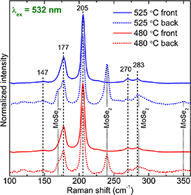
Figure 3. Raman spectra of CZGSe-based solar cells with absorbers annealed at 480 °C and 525 °C measured under 532 nm excitation wavelengths from the front and back side of the devices. Here the peaks indicated with the numbers (peaks positions) belong to the CZGSe phase.
Download figure:
Standard image High-resolution imageTherefore, we conclude that the annealing temperature does not significantly influence the formation of the CZGSe kesterite phase itself but the segregation of extra Ge and Se in secondary phase, which only appears at low temperature. The spectra measured from the back side of the absorber show intense peaks attributable to the MoSe2 phase [29], formed at the back interface of the absorber, together with peaks of CZGSe. The relative intensity of MoSe2 Raman peaks is higher in the sample annealed at 525 °C, indicating a thicker MoSe2 layer at this back interface (see dotted spectra in figure 3). As detected by GD-OES, the Na-signal is also higher compared to the Mo-signal in the sample heated at higher temperature in comparison to the sample annealed at 480 °C. The higher Na content near the Mo contact might enhance the formation of a thicker MoSe2 layer in this region. Previously, Na was found to act as a catalyst, promoting the formation of MoSe2 layer at the back interface of CIGSe-based solar cells [30], which is also observed in the previous work with CZTGSe-based devices [19].
Comparison of the Raman spectra of the CZGSe phase measured at the front and the back side of the absorber layers did not show any significant difference for either sample. This implies that the CZGSe kesterite phase is quite homogenous throughout the sample depth, while the changes in elemental distribution found from GD-OES, mainly for the sample annealed at 480 °C, are related to the formation and inhomogeneous distribution of GeSe2.
Figure 4 shows cross-sectional SEM images of both samples. The most striking observation is the larger grain size for the absorber annealed at higher temperature, as expected because the growth of the grains is thermally activated [31]. Apart from that, in both samples the absorber morphology is characterized by a compact structure, free of pin-holes.
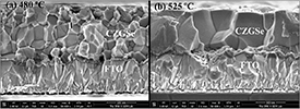
Figure 4. Cross-sectional SEM images of CZGSe/Mo/V2O5/FTO/glass structure with the absorber layer annealed at (a) 480 °C and (b) 525 °C.
Download figure:
Standard image High-resolution imageSolar cell devices were finished using the absorber layers investigated. Figure 5 shows J–V characteristics of the best CZGSe-based solar cells with the absorber layers deposited at 480 °C and 525 °C measured in the dark and under illumination. It can be observed that the device annealed at 480 °C presents a more significant cross-over between the illuminated and dark curves at Jcross = 5.5 mA cm−2, while Jcross increases up to 6.6 mA cm−2 when CZGSe was annealed at 525 °C. Mitzi et al [32] reported that this cross-over can be linked to a current blocking back contact between Mo and CZTSSe, which can suppress the hole transport. As stated above, we observed that the higher annealing temperature resulted in a higher accumulation of Na near the Mo back contact that allows for a thicker MoSe2 layer. The different MoSe2 layer formed at the back interface in both devices might therefore be responsible for the different behaviour of these J–V curves. The fact that the cross-over in the dark and illumination curves is still present in the 525 °C sample might indicate that the back contact is not completely optimized yet. On the other hand, this cross-over behaviour could also be due to a non-optimal kesterite/buffer interface. It has been observed that the presence of GeSe2 secondary phase becomes more important at the surface of the CZGSe annealed at 480 °C, which presents the most significant cross-over.

Figure 5. Light and dark J–V data of the best CZGSe-based solar cells deposited onto semi-transparent back contacts.
Download figure:
Standard image High-resolution imageTable 2 shows the PV parameters of the best devices shown in figure 5. A higher efficiency of 5.3% is obtained for the device with CZGSe deposited at 525 °C, mainly due to a higher VOC and fill factor FF. The lower cross-over effect and the improved VOC in this device can explain the better FF. A maximum performance of 4.2% is achieved for the CZGSe-based device with the kesterite layer annealed at 480 °C. Therefore, the improvement of the device interfaces (increase of the thickness of MoSe2 layer at the back and reduction of the GeSe2 secondary phase at the front) and the higher quality of the bulk absorber layer (larger grain size and significant decreased of GeSe2 phase) by increase of the annealing temperature, are fundamental to further enhance the device performance.
Table 2. PV parameters of the best CZGSe-based solar cells using kesterite absorber layer annealed at 480 °C and 525 °C. The Jsc determined from EQE spectra as well as the efficiency calculated using this value (active area) appear in bracket.
| Absorber | VOC (mV) | JSC (mA cm−2) | FF (%) | η (%) |
|---|---|---|---|---|
| 480 °C | 516 | 13.9 (13.6) | 58.8 | 4.2 (4.1) |
| 525 °C | 585 | 14.7 (16.1) | 61.4 | 5.3 (5.8) |
Figure 6(a) shows EQE spectra of the devices shown in figure 5 and table 2. A higher EQE starting from approximately 490 nm is measured for the CZGSe annealed at higher temperature, in agreement with the higher short circuit current density JSC. The integrated JSC determined from EQE appears in table 2, leading to an active area efficiency of 5.8% for the device annealed at 525 °C. EQE curves start to decrease starting from around 500 nm in both devices, indicating losses due to optical reflection and/or carrier collection suggesting that the CdS/CZGSe interface and CZGSe bulk material are not fully optimized, especially for the absorber synthesized at lower temperature. The stronger drop of EQE in the case of the CZGSe layer annealed at 480 °C can be related to the significant presence of GeSe2 secondary phase, being detrimental for the carrier collection. IQE was also determined from the reflectance measurements of the solar cells. An increased spectral response until 800 nm wavelength is observed for both solar cells (see figure 6(a)). Short circuit current densities of 15.5 mA cm−2 and 17.8 mA cm−2 are calculated from IQE measurements for CZGSe-based solar cells with the absorber layer annealed at 480 °C and 525 °C, respectively. Therefore, these results suggest that the use of an antireflection coating could enhance the device efficiency up to 4.7% and 6.4% for CZGSe heated at 480 °C and 525 °C respectively. EQE spectra were measured under reverse bias (−1 V), increasing the EQE response in the range above 500 nm accordingly (see figure 6(b)). The difference between the EQE spectra without bias and with the reversed bias indicates a poor carrier collection, because of the increased depletion width under −1 V [33], which is more significant for the device with the absorber layer annealed at 480 °C with smaller grain size. This implies that the collection efficiencies are probably limited by very low carrier lifetime, which is found to be a more general problem limiting the VOC in kesterite-based devices [32].
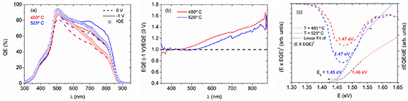
Figure 6. (a) EQE spectra without and under reverse bias of the best devices using CZGSe annealed at 480 °C and 525 °C. IQE spectra is also plotted for both devices. (b) EQE (−1 V)/EQE (0 V) ratio. (c) Determination of band gap energy of the CZGSe from EQE measurements using the linear fit of (E × EQE)2 and the inflection point of EQE at the long wavelength (minimum of the derivative dEQE/dE).
Download figure:
Standard image High-resolution imageThe optical band gap energy Eg of CZGSe has been determined from EQE using two methods (figure 6(c)). The first one was from the linear fit of (E × EQE)2 versus E, and the second from the inflection point of EQE at long wavelengths (minimum of dEQE/dE), as shown in figure 6(c). As reported in literature [34], the derivative method gives similar values to that obtained by optical absorption measurements, while the values obtained by the linear fit method are more accurate in samples with band gap energy gradient, which is not the case here. Slightly higher Eg are obtained by using the linear fitting method for both devices, but all the values are very consistent and lie between 1.45 and 1.47 eV. Therefore, the band gap energy of both absorber layers is not responsible for the difference in VOC between both devices. As mentioned before, the presence of high amounts of GeSe2 was detected in the CZGSe synthesized at lower temperature, which could influence the lower absorption in the bulk of the absorber layer and limit the VOC and final device performance. The lower VOC of this device agrees with the higher difference in EQE (−1 V)/EQE (0 V); however, more investigation is necessary to conclude about the origin of that.
Figure 7 shows the total, straight-through and diffuse transmittance measurements of both CZGSe absorber layers grown on Mo/V2O5/FTO/glass structure. Although the straight-through transmission is lower for the absorber annealed at 525 °C, the diffuse one is higher because of its larger grain size, leading to a higher total transmittance. The larger grain size increases the roughness of the surface leading to an increase of the light scattering. It should be noted that this scattered light can be still absorbed by the bottom solar cell in tandem devices, and therefore it is not lost. This result shows that higher annealing temperature has beneficial effect to the CZGSe-based devices without significant losses in total transmitted light.

Figure 7. Total, straight-through and diffuse transmission measurements of CZGSe/Mo/V2O5/FTO/glass structure.
Download figure:
Standard image High-resolution image
Obviously, highly transparent kesterite-based solar cells are desirable to be used for a tandem device, for bifacial cells or for BIPV applications. Therefore, it is necessary to find an optimal compromise between high efficiency and high transparency, which is a great challenge. Different strategies can be envisioned to enhance device performance and transparency. Among others, we point out the following strategies:
- Consideration of other back contact configurations, as investigated by Espindola-Rodriguez et al [17].
- Optimization of the Na-supply, for example, the thickness of the NaF layer, which probably plays an important role in the development of an optimized back interface, as observed in CIGSe-based solar cells [35].
- Optimization of the kesterite absorber layer: reduction of the thickness that allows for higher transparency without losing device efficiency [36], alternative thermal processes, increase of Eg by addition of S [37, 38] to gain in transparency.
- Alternative buffer layers to enhance the buffer/kesterite interface and band alignment [39].
- Optimization of the window layer (reduced absorption).
- Introduction of an anti-reflecting coating to reduce optical losses.
The optimization of these parameters can be crucial to achieve the goal of high performance and transparency together. This work has shown some first steps, indicating the potential of semi-transparent CZGSe-based devices with a promising future, but there is still much to do and investigate.
4. Conclusions
CZGSe thin films have been grown by co-evaporation followed by an annealing process at maximum temperature of 480 °C or 525 °C. The effect of the annealing temperature on the transmittance, compositional, structural and vibrational properties of the absorber layer grown on a semi-transparent Mo/V2O5/FTO/glass structure has been investigated. The CZGSe layer annealed at 525 °C is characterized by a larger grain size, a Cu-poor and Zn-rich composition and a uniform distribution of the elements throughout the absorber layer. However, the CZGSe treated at 480 °C presented a Zn-poor composition, the co-existence of kesterite with a GeSe2 secondary phase, the latter also being present in the absorber annealed at higher temperature, but in less proportion. Raman spectroscopy confirmed the formation of a MoSe2 layer at the back interface, with a higher thickness for the CZGSe annealed at 525 °C. Moreover, good crystalline quality of the kesterite phase was found for both samples from the spectra measured at the front and back side of the absorber. This yields that annealing temperature was mainly influencing the size of the grains, the formation of the secondary phase at the front interface and a MoSe2 phase at the back, rather than had a significant influence to the CZGSe kesterite phase itself. J–V characteristics of the solar cells showed a reduced cross-over between the illuminated and dark curves, as well as a higher spectral response when CZGSe was synthesized at the highest temperature. The origin for that could be in the differently thick MoSe2 layers formed between the kesterite and the back contact; however, other explanations as e.g. a reduction of the amount of the GeSe2 phase in the bulk and at the surface region of the absorber layer and the larger grain size can play an important role as well. A higher total-area efficiency of 5.3% (active area: 5.8%) and Eg = 1.47 eV was achieved for the CZGSe annealed at 525 °C. A higher total transmittance was also obtained for the absorber heated at the highest temperature. Presenting the first efficient semi-transparent CZGSe-based solar cell is a crucial first step of the development.
Acknowledgments
This work was supported by Spanish Ministry of Science, Innovation and Universities Project WINCOST (ENE2016-80788-C5-2-R), Project RTI (2018-096498-B-I00, AEI/MICINN/ERDF) and European Project INFINITE CELL (H2020-MSCA-RISE-2017-777968). Authors from IREC belong to the SEMS (Solar Energy Materials and Systems) Consolidated Research Group of the 'Generalitat de Catalunya' (Ref 2017 SGR 862). MG and MP acknowledge the financial support from Spanish Ministry of Science, Innovation and Universities within the Juan de la Cierva (IJC2018-038199-I) and Ramón y Cajal (RYC-2017-23758) Fellowships respectively. MGP also acknowledges funding from AEI/MICINN (PTA2019-016763-I). The authors acknowledge the service from the MiNa Laboratory at IMN-CSIC, and funding from CM (project S2018/NMT-4291 TEC2SPACE), MINECO (project CSIC13-4E-1794) and European Union (FEDER, FSE). The authors would also like to thank Professor Rosalia Serna from IO-CSIC for helpful discussion.
Data availability statement
All data that support the findings of this study are included within the article (and any supplementary files).