

Abstract
The emergence of hybrid metal halides (HMH) materials, such as the archetypal CH3NH3PbBr3, provides an appealing material platform for solution-processed spintronic applications due to properties such as unprecedented large Rashba spin-splitting states and highly efficient spin-to-charge (StC) conversion efficiencies. Here we report the first study of StC conversion and spin relaxation time in MAPbBr3 single crystals at room temperature using a spin pumping approach. Microwave frequency and power dependence of StC responses are both consistent with the spin pumping model, from which an inverse Rashba–Edelstein effect coherence length of up to ∼30 picometer is obtained, highlighting a good StC conversion efficiency. The magnetic field angular dependence of StC is investigated and can be well-explained by the spin precession model under oblique magnetic field. A long spin relaxation time of up to ∼190 picoseconds is obtained, which can be attributed to the surface Rashba state formed at the MAPbBr3 interface. Our oblique Hanle effect by FMR-driven spin pumping technique provides a reliable and sensitive tool for measuring the spin relaxation time in various solution processed HMH single crystals.
Export citation and abstract BibTeX RIS

Original content from this work may be used under the terms of the Creative Commons Attribution 4.0 licence. Any further distribution of this work must maintain attribution to the author(s) and the title of the work, journal citation and DOI.
1. Introduction
The ability to transduce and manipulate an electric charge current into a corresponding spin current, and vice versa, is central to the field of spin-orbitronics [1, 2]. To this end, a great deal of research has focused on the generation [3–6], manipulation [7–11], and detection [12–14] of the electron spin by means of spin–orbit coupling (SOC). Interconversion between electron spin and charge is typically accomplished via the spin Hall effect (SHE) and inverse spin Hall effect (ISHE), in which a three-dimensional (3D) charge current ( ) is injected into a nonmagnetic material with strong SOC, resulting in the generation of a transverse 3D spin current (
 ) with orthogonal spin polarization direction S [14]. The efficiency of this conversion is proportional to the strength of the SOC in the nonmagnetic material, and is represented by the spin Hall angle (
 ), where
  and
and  [15]. Recently, a more efficient spin-to-charge (StC) conversion mechanism has also been discovered in strong SOC materials that lack inversion symmetry, known as the Rashba–Edelstein effect (REE) and inverse Rashba–Edelstein effect (IREE) [16–18]. This process occurs due to the formation of an interfacial 'Rashba splitting state', wherein spin degenerate bands are split in the presence of both strong SOC and the local breaking of inversion symmetry. Unlike the bulk 3D spin-to-charge conversion that occurs in ISHE, under the IREE a 2D charge current (
 ) is generated when there is a sufficient presence of spin accumulation injected from an adjacent ferromagnet into the Rashba interface. In direct analogue to the ISHE conversion relation, the IREE process could be described by
  [19], wherein
  is the IREE 'coherence length' that determines the conversion efficiency through the relation
  where
where  is the Rashba coefficient and
  is the momentum scattering time at the Fermi contour [20]. These Rashba states have been studied in two-dimensional electron gas (2DEG) systems [21] and 3D topological insulators [22], showing great promise for next generation spin-to-charge transduction applications at room temperature.
The recent debut of spintronic studies using hybrid metal halide (HMH) materials [23–27], such as the prototypical material methylammonium lead bromide (CH3NH3PbBr3, MAPbBr3), have attracted an immense amount of research interest beyond their exciting optoelectronic properties for applications in solar cells [28–32], light-emitting diodes [33–35], lasers [36–38], and photodetectors [39–42] etc. They are remarkably defect tolerant, and the presence of heavy elements such as Pb in their inorganic framework leads to exceptionally strong SOC. In addition, they possess broad chemical tunability through chemical substitution of the halide anions and organic cations [43], allowing for synthetic control of the SOC strength, lattice constant, dimensionalities, bandgap, as well as emergent Rashba splitting states [44–47]. These advantageous properties have made the family of HMHs a prime solution-processed material candidate for StC transduction applications. However, the exact description of the Rashba effect in these materials has remained elusive as most studies have utilized thin films whose polycrystalline nature [45], where inversion symmetry is broken not only at film surfaces but also at grain boundaries, complicates the data analysis [48].
One way to unravel the role of the Rashba state in HMH materials is through measurements of the spin lifetime. For this, it is best to study them in their single crystalline form as it is the most pristine embodiment of crystalline matter where properties are more directly related to the presence of SOC from the heavy elements or spin-momentum relations induced by the Rashba state, and less related to the presence of defects such as grain boundaries. A precise and reliable technique for measuring this parameter in HMH materials is the electrical 'Hanle' effect [20]. However, it is impractical to apply the traditional nonlocal magnetoresistance and electrical Hanle measurements in metals, which require solvent-based photo-/e-beam lithography procedures [49], to HMH materials. For this reason, no conventional electrical Hanle measurement has been demonstrated in HMHs at room temperature except for the ultrafast magneto-optical studies that is severely limited to cryogenic temperature operation for the clear demonstration of the Hanle precession in a handful of HMH materials [50]. Measuring the spin lifetime in such HMH materials without the aid of cryogenic environment is an extremely arduous endeavor. The electrical detection of the oblique Hanle effect by a ferromagnetic resonance-driven spin pumping technique—the change of StC conversion corresponds to a suppression of spin accumulation via spin precession under an oblique magnetic field [51]—enables us to obtain the crucial information about spin lifetime at room temperature and convincing proof of spin accumulation without involving destructive nanofabrication processes, and is particularly suitable for the HMH single crystal samples.
Here we demonstrate for the first time a complete spin pumping study on a macroscopic MAPbBr3 single crystal using ferromagnetic resonance (FMR) and spin pumping techniques. The obtained StC signals change as a function of field orientation angle because of the spin-precession under the oblique magnetic field, enabling a first-order estimate of the spin lifetime in the MAPbBr3 single crystal and providing strong evidence for the presence of a surface Rashba state. The application of oblique Hanle spin pumping provides a reliable metrology to study the spin lifetime in the family of solution processed HMH materials, which has been technically challenging for the conventional electrical Hanle measurement due to the inevitable conflicts between solution-based material preparation and nanofabrication procedures.
2. Experimental details
Figure 1(a) shows an optical image of the MAPbBr3 single crystal used for spin pumping measurements. The crystal was grown using an inverse temperature crystallization technique [52] and has approximate dimensions of 3 × 3 × 2.5 mm. 15 nm of Ni81Fe19 (99.99% purity, Angstrom Engineering) was deposited on the top surface of the single crystal using electron beam evaporation with a base chamber pressure of 1 × 10⁻⁷ Torr and deposition rate of 0.2 Å s−1. Silver paste (Ted Pella, Inc.) was applied to the both sides of the crystal to provide electrical contacts for spin pumping voltage measurements, as shown schematically in figure 1(b). X-ray diffraction was used to check the phase purity of the prepared single crystal. Figures 1(c) and (d) show the diffraction patterns obtained for both the single crystal and its powdered form, respectively, revealing a high quality single crystallinity.

Figure 1. (a) Optical image of a MAPbBr3 single crystal with ruler for scale. The sample size is approximately 3 × 3 × 2.5 mm. (b) Schematic illustration of the NiFe/MAPbBr3 single crystal device used for spin pumping measurements, where M denotes the magnetization direction and V is the measured voltage. (c) and (d) X-ray diffraction spectra obtained for MAPbBr3 in both powder and bulk single crystal forms, respectively.
Download figure:
Standard image High-resolution imageFerromagnetic resonance (FMR) was performed at room temperature from 2 to 16 GHz using a commercial NanOSC PhaseFMR spectrometer with a coplanar waveguide, while an GMW electromagnet was used for applying an external magnetic fields. For the spin pumping measurements, microwaves are generated by a Keysight X-Series Microwave Analog Signal Generator at an excitation frequency of 2–16 GHz and microwave power of 50 mW. A transverse dc voltage is electrically detected between two silver paste contacts at opposite ends of the single crystals, recorded by a Stanford SRS530 Lock-In Amplifier. Oblique Hanle effect measurements are performed by rotating the sample and coplanar waveguide with respect to the applied magnetic field using a precision goniometer, by which both the transverse dc voltage and FMR signal can be recorded simultaneously. All the measurements were taken at room temperature.
3. Results
3.1. Broadband ferromagnetic resonance and spin pumping
Figure 2(a) shows the typical FMR spectra obtained at different microwave frequencies for the Ni81Fe19/MAPbBr3 single crystal device, from which values for α, the damping factor, γ, the gyromagnetic ratio, and Ms, the saturation magnetization, are derived. Ms and γ are obtained from the HFMR versus ƒ plots shown in figure 2(b), by fitting to the Kittel equation:  [53], where HFMR is the resonant field. Values for 4πMs and γ for a bare Ni81Fe19 reference sample deposited on a glass substrate are found to be 0.627 T and 191.64 GHz T−1, respectively, which are consistent with those reported in the literature [54]. Damping factors are extracted using the relation,
  where ΔH is the FMR linewidth (HWHM) and ƒ is the microwave frequency.
  is the frequency-independent linewidth contribution arising from inhomogeneities in the ferromagnetic film and single crystal surface. The intrinsic damping parameter, α0, for the bare NiFe reference sample is found to be 5.4 × 10⁻³, while the damping parameter of the Ni81Fe19/MAPbBr3 is found to be 2.1 × 10⁻², as shown in figure 2(c).

Figure 2. (a) FMR spectra of the NiFe/MAPbBr3 bilayer obtained between 2 and 16 GHz. (b) Microwave frequency f plotted as a function of the resonant field HFMR, where the solid curve represents a fit to the Kittel formula. (c) FMR linewidth plotted as a function of microwave frequency for the NiFe/MAPbBr3 (blue) and NiFe reference sample (red).
Download figure:
Standard image High-resolution imageWhen an in-plane magnetic field is applied, the vertical spin current density ( ) that is injected into the NiFe/MAPbBr3 interface under the ferromagnetic resonance may be calculated via the relation [54]:

where  is the spin mixing conductance at the interface determined by
  where
where  is the thickness of the ferromagnetic layer,
  is the microwave field,
  is the effective saturation magnetization of NiFe,
 is the electron charge, and
  is the Planck constant.
Spin pumping measurements are performed at room temperature using the same experimental setup used for the FMR measurement. The voltage generated across the Ni81Fe19/MAPbBr3 device is measured as a function of applied magnetic field at different microwave frequencies and microwave powers, as shown in figures 3(a) and (b), respectively. The obtained dc voltage signal can be decomposed into two parts, a symmetric and an antisymmetric voltage component given by [12]:  where VSym is the spin pumping voltage generated from the StC conversion and VAsym is the Anomalous Hall effect (AHE) contribution from the Ni81Fe19 layer [12]. Flipping of the voltage polarity upon the reversal of the applied magnetic field from +Hres to −Hres provides a strong evidence that the signal is indeed originated from the spin pumping process rather than that from the heating induced artifact which is magnetic field independent [55]. Here, we take the average of VSym for +HFMR and –HFMR as the actual VSP, where
 ![${V}_{SP}=\left[{V}_{Sym}\left(+{H}_{FMR}\right)-{V}_{Sym}\left(-{H}_{FMR}\right)\right]/2.$](https://content.cld.iop.org/journals/2515-7639/3/1/015012/revision2/jpmaterab69b0ieqn25.gif) Figure 3(c) shows the microwave frequency dependence of VSP can be fitted with the equation
Figure 3(c) shows the microwave frequency dependence of VSP can be fitted with the equation ![${V}_{SP}\propto {\left[{\left({M}_{eff}\gamma \right)}^{2}+{\left(4\pi f\right)}^{2}\right]}^{-1/2},$](https://content.cld.iop.org/journals/2515-7639/3/1/015012/revision2/jpmaterab69b0ieqn26.gif) in good agreement with spin pumping model [51]. The decrease in the magnitude of VSP with increasing microwave excitation frequency further proves that the observed Vsp signal does not stem from heating induced artifact, but rather the actual spin pumping induced signals. Figure 3(d) shows the linear dependence of VSP with microwave power, consistent with the spin pumping model in the linear-response regime [56].
in good agreement with spin pumping model [51]. The decrease in the magnitude of VSP with increasing microwave excitation frequency further proves that the observed Vsp signal does not stem from heating induced artifact, but rather the actual spin pumping induced signals. Figure 3(d) shows the linear dependence of VSP with microwave power, consistent with the spin pumping model in the linear-response regime [56].

Figure 3. (a) Spin pumping voltage VSP measured as a function of external magnetic field H for different microwave frequencies (b) VSP measured as a function of H for different microwave excitation powers at a frequency of 6 GHz. (c) Data (symbols) and theoretical fit (line) for VSP measured as a function of microwave frequency. (d) Data (symbols) and theoretical fit (line) for VSP measured as a function of microwave power. The inset shows the calculated IREE length versus microwave power.
Download figure:
Standard image High-resolution image3.2. Oblique Hanle spin precession
We have conducted both field angular dependent FMR and spin pumping measurements, namely performing the spin pumping measurement when applied external magnetic field, H is applied oblique to the film plane by an angle  from 0° to 180°, as shown schematically in figure 4(a). Under the oblique magnetic field, the relation between the external magnetic field angle
  and the angle of the magnetization–precession axis
  is calculated using the Landau–Lifshitz–Gilbert equation, which can be described by [51, 57]:


where  is the applied magnetic field strength under the resonance condition. Figures 4(b) and (c) presents the obtained angular dependence of the FMR and VSP signals, respectively. The resonant fields,
  from the FMR spectra are plotted as a function of
  in figure 4(d). The relation between
  and
and  calculated from equation (2) with the measured value of
  is shown in figure 4(e) [51].

Figure 4. (a) Schematic illustrations of the NiFe/MAPbBr3 bilayer during spin pumping experiments when the external field H is applied out-of-plane by an angle θ. M and Vsp denote the magnetization vector for NiFe and spin pumping voltage, respectively. (b) FMR spectra normalized by resonant field plotted for different magnetic field angles θ. (c) Spin pumping voltage VSP normalized by resonant field plotted for different magnetic field angles θ. (d) HFMR plotted as a function of θ (e) magnetization angle φ plotted as a function of θ according to the Landau–Lifshitz–Gilbert equation with the measured HFMR values. (f) VSP plotted as a function of θ. Fit curves with four different spin-relaxation times (τsf) are shown using equation (4). The solid circles represent experimental data while the solid curve represents the best fit obtained with τsf = 189 ps. The inset shows the same fitting applied to a sample of NiFe (15 nm)/SiO2 where τsf ∼ 18 ps.
Download figure:
Standard image High-resolution image
The oblique magnetization M( ) of the NiFe film at the ferromagnetic resonance injects the pure spin current
  into the MAPbBr3 layer of which spin polarization direction follows the oblique magnetization direction (figure 4(a)). Due to the misalignment between
  and
and  the injected
  in the MAPbBr3 layer under the oblique static external magnetic field precesses and results in a decrease of transverse IREE voltage because of the suppressed spin accumulation via spin precession and dephasing, i.e. the Hanle effect [58, 59]. By increasing the angle of the applied magnetic field, the in-plane component of
  senses a larger out-of-plane field strength that further suppress the spin accumulation, giving rise to a typical characteristic of field angular dependence of the spin pumping voltage [51] if the spin relaxation time, τsf is considerably comparable to or larger than the Larmor precession time
  (
( is the Larmor frequency under the oblique magnetic field). The spin pumping voltage, VSP, is plotted as a function of out-of-plane angle,
  in figure 4(f), allowing us to determine the spin lifetime, τsf, in the MAPbBr3 layer using the Hanle precession model with both ISHE and IREE contributions [51, 60]:
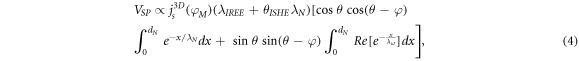
where  is the angular dependent injected spin current density at the interface under the oblique FMR condition given by equation (1) [54], dN is the thickness of MAPbBr3 single crystal (i.e. 2.5 mm) for the bulk ISHE contribution or the nominal thickness of the Rashba surface state (taken as 2 nm) [61],
  is the spin diffusion length in the MAPbBr3 crystal, and
  [51].
[51].
It is noteworthy that equation (4) was originally derived from an equivalent circuit model for the interpretation of field angular dependent ISHE measurements [51]. For simplicity, here both bulk ISHE contribution and surface Rashba induced IREE contribution share the same Hanle precession model but with different nominal thickness and spin diffusion length parameters. The reasoning is that in ISHE, the entire thickness of the NM (i.e.  can be up to 2.5 mm for the thickness of single crystal) contributes to the generated transverse dc voltage: the spin current at a certain depth into the material is related to the spin diffusion length, resulting in a gradual increase of StC conversion when the thickness increases until it saturates [62]. In contrast, at a Rashba surface state, the StC conversion occurs with a constant conversion efficiency only at the surface state as detailed in previous reports [62, 63]. Thus, a constant StC conversion coefficient in the form of IREE coherence length will be assumed. Specifically, at the surface state, the produced 3D spin diffusion will be limited at the 2D surface state, in which the spin diffusion length is simply equivalent to the value of the nominal thickness of the surface state as used in other topological insulator systems [64], i.e.
Four fit curves using different spin-relaxation times (τsf) are shown in figure 4(f) to illustrate how the fitted model curve changes with 
 IREE contribution, and only bulk ISHE contribution with expected low spin lifetime at room temperature (
 [51]), respectively. The best fit curve is produced with τsf = 189 ps, which is determined using the spin lifetime for the Ni81Fe19/MAPbBr3 single crystal with only IREE contribution. For comparison, a similar measurement for the NiFe/SiO2 control sample was also performed (the inset of figure 4(f)). A much smaller spin lifetime of τsf = 18 ps is obtained in stark contrast to the long spin lifetime observed in the MAPbBr3 sample, indicating that the magnetoresistance artifacts from the NiFe layer do not play a dominant role in our measurement. This is further corroborated by a subtle anisotropic magnetoresistance (AMR) signal (ΔR/R < 0.2%) measured in the NiFe layer using the same set up, showing that the AMR contribution to the angular-dependent IREE voltage is negligible.
4. Discussion
Bulk MAPbBr3 forms a disordered cubic structure at room temperature with an average space group symmetry of  This centrosymmetric structure possesses inversion symmetry, and thus should lack any bulk Rashba type effects. However, at the surface or interface this inversion symmetry is necessarily broken and therefore allows for the formation of a surface Rashba state. Indeed, it has been proposed that the giant Rashba splitting previously observed in MAPbBr3 stems from this surface state and not the bulk [27, 65, 66] and recently experimentally proven in the MAPbrBr3 polycrystalline thin film [62]. It is thus tremendously advantageous to utilize single crystals in the analysis of the surface Rashba state, where a single material surface may be isolated and probed and the effects of defects such as grain boundaries is minimized.
In our spin pumping experiments, we use microwave excitation of the NiFe thin film at its ferromagnetic resonance for the generation of a 3D spin current that is subsequently injected into the adjacent MAPbBr3 single crystal. If the predicted surface Rashba state is present at this interface, the spin current may be converted into a corresponding 2D charge current by the IREE process. For FMR measurements, this should manifest as spin current dissipation across interface, namely spin sink behavior resulting in an increase in the damping factor of the bilayer with respect to the isolated ferromagnetic film. This expected phenomenon is confirmed in figure 2(c), where we see that the damping factor obtained for NiFe/MAPbBr3 (2.1 × 10⁻²) is almost four times larger than that of the bare NiFe film (5.4 × 10⁻³). This large increase in damping for the bilayer system is indicative of the presence of a strong spin to charge conversion process, which is further reinforced by IREE measurements. The transverse charge current generated at the interface in response to the injected spin current can be estimated by the relation  where
where  is the length of the device (3 mm) and
  is the total device resistance calculated as
 ![$R=\tfrac{1}{\left[{\sigma }_{MAPbBr3}{d}_{MAPbBr3}+{\sigma }_{NiFe}{d}_{NiFe}\right]},$](https://content.cld.iop.org/journals/2515-7639/3/1/015012/revision2/jpmaterab69b0ieqn57.gif) where
where  is the conductivity of the MAPbBr3 single crystal,
  (1.17 × 10⁻⁵ Ω cm) is the conductivity of the NiFe layer,
  is the thickness of the MAPbBr3 single crystal and
  (15 nm) is the thickness of the NiFe layer. As described by the relation
  by comparing the
  obtained from FMR and
  obtained from IREE, we may extract the IREE coherence length which we find to be
  that remains constant as a function of microwave power (inset of figure 3(d)). This value is comparable to the coherence lengths found in YIG/Bi2Se3 (∼35 pm) and NiFe/Bi2Se3 (60 pm), although it is much smaller than those found in systems such as Bi/Ag (100–400 pm) and α-Sn (2100 pm) [18, 19, 67, 68].
To provide further evidence for the presence of an interfacial Rashba state in our NiFe/MAPbBr3 bilayer, we directly determine the spin lifetime τsf and compare it to other systems. We accomplish this by performing both FMR and IREE measurements as a function of external magnetic field angle θ. By plotting the obtained spin pumping voltage as a function of θ and fitting the result to equation (2), we are able to extract a numerical value for the spin carrier relaxation time at the interface. The spin relaxation time of τsf = 189 ps obtained for the NiFe/MAPbBr3 system is much larger than that in the NiFe sample (SiO2/NiFe) alone, where τsf = 18 ps (see the inset of figure 4(f)), or even in the NiFe/Pt bilayer sample, where τsf = 33 ps. Whereas a larger spin relaxation time in the NiFe film is probably ascribed to the self-ISHE response originated from the potential surface state formed between the NiFe and SiO2 substrate (τsf (NiFe only) = 0.025 ps would be expected for the pure NiFe film [51]), the results from these control samples further confirm that the obtained transverse voltage signals in the NiFe/MAPbBr3 is unlikely originated from the self-ISHE response from the NiFe film or from spin-rectification effects [69–71].
The large increase in spin relaxation time for NiFe/MAPbBr3 can be attributed to the presence of a surface Rashba state formed at the NiFe/MAPbBr3 interface where the breaking of inversion symmetry leads to the formation of two degenerate spin contours with opposite helicity. A spin carrier injected into this environment is unable to undergo rapid spin relaxation when a strong correlation between momentum and spin is locked within these helical contours. In contrast to a usually short spin lifetime if the spin flip increases with the scattering rate increasing following the Elliott–Yafet mechanism [72], a long spin lifetime would be anticipated if the Rashba state dominates the StC interconversion where the spin lifeime is likely to be inversely proportional to the momentum scattering time (τp) via the D'yakonov–Perel mechanism [73]. Therefore, the spin lifetime in HMHs obtained by both the FMR-driven spin injection is much longer than the momentum relaxation time τp ∼0.5 fs [74]. This comparison also provides additional support for the presence of an interfacial Rashba state, where we would expect similar relaxation times if the signal were coming from a pure ISHE process. We note that this spin relaxation time is also much longer than what would be expected if the relaxation process was dominated by SOC from Pb atoms in the perovskite's inorganic framework, where ultrafast optical measurements have estimated values of  [23, 61].
We are unaware of any other reports on the spin lifetime in MAPbBr3 single crystals at room temperature with which we could compare our experimentally obtained value of τsf = 189 ps. However, there have been some reports on polycrystalline MAPbBr3 thin films measured at low temperature as well as several recent theoretical studies on MAPbBr3 and MAPbI3 single crystals [27, 65, 66, 75, 76]. Wang et al used partial circularly polarized photoluminescence (CPL) to measure spin lifetime via the optical Hanle effect in MAPbBr3 thin films at low temperature, with measured relaxation times of τsf = 240 ps at 77 K that reduces by an order of magnitude at 110 K [76]. Wang et al similarly measured optical Hanle responses in MAPbBr3 thin films at low temperature using CPL, finding that τsf = 491 ps at 10 K [75]. In addition, they measured electrical Hanle responses for the thin film in a spin valve configuration to obtain a spin relaxation time of τsf = 936 ps at 10 K [75]. The large reduction in spin lifetime with increasing temperature has also been considered theoretically [66], where it is shown that τsf may be reduced by over two orders of magnitude between 10 and 300 K. Thus, our obtained value of τsf = 189 ps for MAPbBr3 at 300 K is eminently remarkable. Please note this estimated value could be larger since the dynamical spin injection method used in this paper, the spin lifetime may be reduced by coupling of the spins at the surface of the MAPbBr3 single crystal to the adjacent NiFe layer [77, 78].
By considering the presence of a surface Rashba state where the signals measured during spin pumping experiments will be coming from the dominant IREE process, the corresponding Rashba coefficient  could be calculated by combining the obtained IREE length (
 ) with a previously calculated value for the spin-momentum scattering time at the Fermi contour
  [77] using the relation
  Using these parameters, we derive a value for the Rashba coefficient of
  This value is comparable in magnitude to the
  obtained from previous spin pumping measurements performed on polycrystalline MAPbBr3 films measured at room temperature [62], although it is lower than the massive
  previously reported based on ARPES measurements of MAPbBr3 single crystals [44].
5. Conclusion
In summary, we report the first spin pumping study on the NiFe/MAPbBr3 single crystal device at room temperature. The obtained IREE coherence length  is comparable in order of magnitude to IREE lengths measured in several topological insulator and 2D systems by similar spin pumping approaches [19, 79–82]. By measuring both FMR and spin pumping signals as a function of out-of-plane external magnetic field angle, an unprecedentedly long spin lifetime τsf = 189 ps at room temperature is obtained, exceeding the presumable short spin lifetime induced by heavy elements in HMH materials. The enhanced spin lifetime is attributed to the presence of an interfacial Rashba state at the NiFe/MAPbBr3 interface. We hope that these results will initiate additional studies of interfacial Rashba effects in various HMH single crystals for future solution-processed spin-to-charge transduction applications.
Acknowledgments
SY, EV and DS are grateful for support from the startup funds provided by North Carolina State University and NSF Grant No. ECCS-1933297. Sample preparation and characterization were partially supported by NC State University-Nagoya Research Collaboration grant.
Author Contribution
D S and A A conceived this study and the experiment. S Y and E V fabricated the devices, measured the FMR, spin pumping, oblique Hanle effect, and calibrated rf field. T W provided the single crystals. E V, S Y, and D S wrote the text. D S and A A were responsible for the project planning and group managing. All authors discussed the results, worked on data analysis and manuscript preparation. The authors declare no competing financial interests.