

Abstract
Two-dimensional (2D) materials have emerged as the ideal candidates for many applications, including nanoelectronics, low-power devices, and sensors. Several 2D materials have been shown to possess large Seebeck coefficients, thus making them suitable for thermoelectric (TE) energy conversion. Whether even higher TE power factors can be discovered among the ≈2000 possible 2D materials (Mounet et al 2018 Nat. Nanotechnol. 13 246–52) is an open question. This study aims at formulating selection rules to guide the search for superior 2D TE materials without the need for expensive atomistic simulations. We show that a 2D material having a combination of low effective mass, higher separation in the height of the step-like density of states, and valley splitting, which is the energy difference between the bottom of conduction band and the satellite valley, equal to 5 kBT will lead to a higher TE power factor. Further, we find that inelastic scattering with optical phonons plays a significant role: if inelastic scattering is the dominant mechanism and the energy of the optical phonon equals 5 kBT, then the TE power factor is maximized. Starting from a model for carrier transport in MoS2 and progressively introducing the aforementioned features results in a two-orders-of-magnitude improvement in the power factor. Compared to the existing selection rules or material descriptors, features identified in this study provide the ability to comprehensively evaluate TE capability of a material and helps in identifying future TE materials suitable for applications in waste-heat scavenging, thermal sensors, and nanoelectronics cooling.
Export citation and abstract BibTeX RIS
Increase in demand for energy sources inspired a vigorous search for new and efficient technologies that can maximize the utilization of existing resources. Recovering waste heat to generate electricity using thermoelectric (TE) materials is a viable path to increase efficiency in existing power generation methods, power wearable sensors, and even supply some of the energy needs in buildings [1]. However, doings so will require materials with high TE power factor that will maximize TE energy conversion efficiency. The efficiency of TE conversion is measured in terms of the dimensionless figure-of-merit [2] ZT = S2σ T/(κe + κp), where σ is electrical conductivity, S is Seebeck coefficient, κe is electronic thermal conductivity, and κp is lattice (phonon) thermal conductivity. Controlled engineering of materials by introducing grain boundaries [3, 4], surface roughness [5–7], interface scattering [8–10], and alloy mass disorder [11–13] reduces κp without significantly changing the electronic transport properties. For maximum enhancement, all of these techniques can be combined in hierarchical nanostructuring [14, 15]. Many TE materials studied thus far rely on some variant of this strategy for reducing κp to improve ZT.
On the other hand, the product S2σ is referred to as power factor and it is mostly dependent on the electronic band structure of material; increasing the power factor or discovering new materials with intrinsically high power factors also improves ZT. To achieve that, a broad swath of approaches, ranging from band-engineering techniques like moving to low-dimensional materials [16–18], to modulation doping [19, 20], electron filtering [21], and electrostatic gating [22] have been proposed. One of the factors that limits our ability to improve power factor by band engineering is the strong coupling between S and σ. Especially in semiconductors, they have opposite behavior with respect to the carrier density and cannot be tuned independently:  so increasing carrier concentration to boost σ also brings the Fermi level closer to the band edge, lowering S. Hence, careful selection of materials with desired properties is required in order to discover new materials with an intrinsically higher power factor. Once such materials are discovered, their ZT could be further improved via aforementioned extrinsic techniques to lower the lattice thermal conductivity; materials with both a large power factor and a large lattice thermal conductivity can be often be further engineered with minor impact on the electronic properties. Towards this end of identifying new materials with high power factors, previous studies proposed simple material property criteria to narrow the search time for identifying the bulk materials or compounds. Among them, the widely accepted criteria for bulk materials are low effective mass [23, 24], a band-gap ≈10 kBT [24–26], high band degeneracy [24, 27], and a carefully tuned composition [28] or a complex unit cell [29]. Mahan and Sofo derived that a delta-function TDF is ideal [17]. Subsequently, Zhou et al showed that, for low dimensional materials, a window-like TDF with a narrow transport bandwidth [30] ≈5 kBT is favorable; however, the optimal bandwidth [31] and bandgap [32] depend on how scattering processes were modeled.
More sophisticated material descriptors or parameters have been proposed to combine different material properties that can be used to evaluate a material's TE capabilities. One of the first is the B-factor introduced by Chasmar and Stratton [33], that can be used as a material descriptor independent of the carrier density (therefore independent of the Fermi energy). B-factor, sometimes also denoted by β, is a material dependent parameter that combines the intrinsic electronic and phononic properties, including mobility, thermal conductivity, and effective mass, into a single parameter that can be used to evaluate a material's TE capability. It is related to ZT via ZT = uβ/(vβ + 1), where u and v depend on the carrier concentration of the material, which is normally optimized via doping to maximize ZT. A material with a larger β and optimal carrier density was shown to provide higher ZT. Subsequently, to understand the anisotropy contribution to TE performance, the b-factor [34, 35] was defined by expanding the B-factor (β) to include any form of band structure and band degeneracy. The b-factor is defined as ![$b={{BF}}_{1/2}\left[({E}_{F}-{E}_{C})/({k}_{B}T)\right]$](https://content.cld.iop.org/journals/2515-7639/3/1/015005/revision2/jpmaterab4600ieqn2.gif) , where F1/2 is a Fermi–Dirac integral of order 1/2, EF is the Fermi energy and EC is the conduction band edge. The higher band degeneracy requirement for high performing TEs [24, 28] is often proved using a simple constant relaxation time approximation or constant mean-free-path approximation. First principles band structure calculations, along with comprehensive electron–phonon scattering rates, improved our understanding of the effect complex band structures and band engineering on TE properties [36, 37]. In a material with multiple anisotropic valleys, the relative strength of intra- versus inter-valley electron–phonon scattering was shown to control the TE performance more than the degeneracy alone [34]. Parameters such as the Fermi surface complexity factor was then proposed to quantify the effect of anisotropy and band degeneracy on TE performance in complex band structure materials [38].
, where F1/2 is a Fermi–Dirac integral of order 1/2, EF is the Fermi energy and EC is the conduction band edge. The higher band degeneracy requirement for high performing TEs [24, 28] is often proved using a simple constant relaxation time approximation or constant mean-free-path approximation. First principles band structure calculations, along with comprehensive electron–phonon scattering rates, improved our understanding of the effect complex band structures and band engineering on TE properties [36, 37]. In a material with multiple anisotropic valleys, the relative strength of intra- versus inter-valley electron–phonon scattering was shown to control the TE performance more than the degeneracy alone [34]. Parameters such as the Fermi surface complexity factor was then proposed to quantify the effect of anisotropy and band degeneracy on TE performance in complex band structure materials [38].
In an effort to formulate a metric that can help to identify materials with single cut-off energy, as originally proposed by Mahan [39], the shape factor (SF) was proposed as a measure of the asymmetry in the density of states (DOS) [40]. SF, for which we give the explicit formula later in the text, is closest to unity when the DOS has abrupt changes and lower when the DOS is smooth and gradual, which follows the conventional wisdom that abrupt changes near the Fermi level lead to better TE properties. A high throughput search among the known compounds confirmed that the SF should approach unity to maximize ZT [40]. The required shape for the DOS to achieve it resembles a step function, which is also the shape of the DOS in 2D materials with a parabolic bandstructure. With the advent of new 2D materials like graphene and single-layer transition metal dichalcogenides (TMDCs), the TE efficiency of these materials has garnered increasing interest. Even though reports suggest an improvement in the power factor of these materials [41–43], with some of the highest power factors ever reported being in graphene encapsulated with hexagonal boron nitride (hBN) [44], high lattice thermal conductivity restricts materials like graphene from achieving higher ZT. Apart from graphene, hBN, and TMDCs, there are many other 2D materials that have exceptional electronic and thermal properties, with the total number of potentially stable 2D van der Waals materials approaching 2000, and a few exhibit good power factor as well. But it is neither obvious which among them are good starting points for TE studies nor is it feasible to synthesize and test every 2D material. We need more insight into the relation between material parameters and TE efficiency, which can help in formulating the material selection rules for new efficient TE materials. Using publicly available material databases, studies [45–47] have predicted numerous new materials with weak van der Waals forces that can be exfoliated into single-layer forms With this extensive and growing knowledge, there is a need to explore the possibility of their use in future TEs.
In our recent study [18], we simulated transport in the inversion layer of a gated silicon-on-insulator device, where the DOS was two-dimensional due to confinement of carriers. We found that inelastic scattering from optical phonons and transitions between subbands are the dominant mechanisms and operating the device in a regime where both equal 5 kBT significantly enhances the TE power factor. There is a need for further research aimed at formulating more complete material descriptors in 2D materials to identify potential candidates with high power factors. The main aim of this study is to use the distinct features of 2D materials and formulate simple yet powerful material selection rules that can provide guidance and identify candidates with high intrinsic power factor for further computational study, synthesis, and measurements. We focus on those material parameters, such as effective mass and deformation potentials, that are easily available in existing 2D materials databases or that require relatively computationally inexpensive first principles calculations in order to reduce the time required for initial evaluation and screening of materials for higher TE performance. Our focus is on semiconducting parabolic-band 2D materials with a step-like DOS and strong inelastic and intravalley scattering. We identify combinations of materials properties that lead to improvements in the power factor by restricting the energy 'bandwidth' of those electrons that contribute to transport but do not have enough energy to participate in inelastic and intervalley scattering. Our approach is one avenue through the vast field of new 2D materials toward more efficient TEs with higher intrinsic power factors and does not eliminate other complementary avenues via extrinsic modification, such as reducing lattice thermal conductivity or forming vertical and lateral heterostructures [48].
Improving the power factor requires identifying the material parameters that simultaneously effect the Seebeck coefficient and electrical conductivity. Starting from the Boltzmann transport equation under the relaxation time approximation and assuming a small deviation from equilibrium, S and σ are be related to the transport integrals as [22]


where L(α) is the transport integral and σn(E) is the transport distribution function (TDF), sometimes referred to as the differential conductivity; furthermore, EF is the Fermi energy, En is the energy of the bottom of valley n, Dn(E) is DOS of that valley, τn(E) is the energy-dependent relaxation time, and vn(E) is the group velocity of the carriers. The Fermi window ∂f0/∂E is symmetric about EF and has a spread of about 10 kBT. The relaxation time of the carriers depends on dominant scattering mechanisms in the material and has varying dependency on energy (E). Assuming that the scattering completely randomizes the transport, the relaxation time is calculated by taking an inverse of the sum of all the scattering rates.
In the effective mass approximation, both carrier velocity and the DOS can be obtained from the effective mass of a particular (main or satellite) valley and the carrier energy. Now observing the transport integral, it is apparent that TDF has to be maximized to improve σ. On the other hand, it was shown that a δ-shaped [17] or narrow-bandwidth [30] TDF is needed for maximum achievable S. But in realistic conditions, a delta-shaped or even narrow TDF is not feasible in 3D materials due to the square-root dependence of both the relaxation time (τn) and DOS (Dn) on energy, stemming from the parabolic bands, which cancel each other's gains (as τn ∝ 1/Dn). In our previous work, we proposed an alternative approach [18] using an extrinsic 2D material, in which quantum confinement in the material plane causes a step-like DOS with a separation of Ecs between subbands. We further found that this effect is enhanced when inelastic scattering is the dominant mechanism. The delay in the onset of inelastic scattering, where  , creates a window of energies from the bottom of the conduction band up to Eph where only elastic scattering occurs. The sharp onset of inelastic processes above Eph means that scattering, and with it the TDF is much higher for carriers below Ecs = Eph and lower for energies above this cut-off, which results in a narrow TDF function with a limited energy bandwidth (E < Ecs = Eph) over which most of the transport occurs. This, in addition to
  in the parabolic bands, gives a narrow window-like shape to the TDF, where most of the transport occurs in a restricted range of carrier energies, as illustrated schematically in figure 1. To simultaneously improve S and σ, the Fermi window should coincide with the TDF. Maximizing this overlap of the half-window width of 5 kBT around EF requires TDF to be 5 kBT wide and
  . Using this approach, we showed a peak enhancement [18] in S at low temperatures in an inversion layer created by confinement that has a step-like DOS.

Figure 1. Schematic to show the parameters defined by the band structure and DOS of a 2D material. The step-like DOS along with the inelastic scattering of carriers results in window-shaped TDF with a restricted energy bandwidth. The approach used in our study is to maximize the power factor by matching window-shaped TDF and Fermi window.
Download figure:
Standard image High-resolution imageHere we extend our approach to intrinsic 2D materials and formulate selection rules that can be used to shortlist candidate 2D materials with potentially higher power factors. As discussed above, the important components to be optimized are TDF (which include  (E), Dn(E), and vn(E)) and the Fermi window. Table 1 summarizes the contributing factors to TDF for single valley in two different band profiles possible in 2D regime: a Dirac material (graphene) and a semiconducting material (such as MoS2). The electronic band structure of a Dirac material can be defined using massless Dirac equation with a Fermi velocity of vF, while for the semiconducting 2D material, we use the effective mass approximation (effective mass of
  ) with elliptical valleys in the conduction band. This results in massless DOS for Dirac material, and an effective-mass-dependent DOS for semiconducting material with a band degeneracy of
  . Also,
  (E) is constant for Dirac materials and linearly dependent on energy (
 ) for the semiconducting material with parabolic bands.
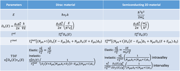
Table 1. Comparison of important material parameters between a Dirac material and a semiconducting 2D material.
|
The scattering of carriers especially from phonons determines the relaxation time (τn) used to calculate TDF. Carrier scattering from phonons can occur in two forms: elastic and inelastic scattering. Elastic scattering, where there is little or no change in the energy of carriers, is generally from acoustic phonons due to their low energy. The elastic scattering rate (Γel) is proportional to the density of final states, which depends on Dn(E) of the band, and a pre-factor Γ0, which is proportional to deformation potentials (Ξ0). On the other hand, inelastic scattering (Γinel) involves emission or absorption of phonons by carriers, resulting in a change of their energy. Controlling the relative strength of these two processes by targeting materials with a small acoustic and large optical phonon deformation potentials helps in achieving a narrow TDF. Δ1 (for emission) and Δ2 (for absorption) are used to make sure that the energy conservation is achieved in inelastic scattering. In this work, we seek to identify the properties of 2D materials that are intrinsically good candidates for TE applications. We include acoustic phonons as the source of quasi-elastic scattering; however, in realistic 2D materials, the presence of charged impurities can be another source of elastic scattering. Its impact on TE performance is detrimental as it reduces mobility without enhancing the Seebeck coefficient, somewhat analogous to our acoustic phonons. Ongoing developments of fabrication techniques, better substrates, and encapsulation by hexagonal boron nitride (hBN) [44] have been shown to reduce the effect of impurities and could be applied to future 2D materials as well. As shown in table 1, inelastic scattering in 2D materials can occur in the form of intervalley and intravalley transitions. Intervalley transitions require carriers from one valley (with DOS of Di(E)) to other valley (with DOS of Df(E) and Z represents number of available valleys).
In Dirac materials, inelastic scattering from both intravalley and intervalley is proportional to the ratio of initial and final Dn(E), while in a semiconducting material, intravalley scattering is independent of Dn(E), but intervalley scattering has the same dependence as a Dirac material. The linear DOS and a constant vn(E) in Dirac materials result in a linear TDF. Graphene, when encapsulated by hBN to improve mobility, has been shown to have a high TE power factor [44], about four times higher than MoS2. While both Dirac and semiconducting 2D materials can exhibit good TE performance, our focus here is on the further enhancements that could be observed in 2D materials in which inelastic phonon scattering is strong and leads to a restricted transport bandwidth. Inelastic scattering, primarily from electron–electron interactions, has been shown to play a role in enhancing the thermopower of graphene [49] beyond values expected based on the Mott formula, valid for transport dominated by elastic processes. The bipolar nature of the transport near the Dirac point, stemming from the absence of a band-gap, somewhat limits their Seebeck coefficient; the record-high power factor of graphene stems largely from high carrier mobility after encapsulation by hBN to mitigate impurity scattering. Since Dirac materials lack a bandgap and typically do not have satellite valleys near the Dirac point, optical phonon emission is always possible while intervalley scattering rarely occurs. Consequently, the type of enhancements that we study in this work are less effective in identifying Dirac materials with even higher power factors. Hence, the rest of our analysis is focused on semiconducting 2D materials with parabolic bands.
Consolidating the variables to be analyzed, we divide them into two categories: parameters that control (a) the width and (b) the height of the TDF. The width of the TDF depends on the onset of inelastic scattering: optical phonon emission is significantly more likely than absorption by a ratio  , where Nph is the Bose–Einstein distribution function of phonons. An electron must have at least E > Eph kinetic energy to emit the phonon, the onset of emission causes a sharp drop in the TDF which can be tuned by phonon energy. In addition to step-like DOS and Eph, the separation between main and satellite valleys (Ecs) also determines the width of TDF through scattering into the satellite valley, as shown schematically in figure 1. Along with controlling the width of TDF, Eph and Ecs help to maximize the Fermi window utilization. Dn(E), which depends on the effective mass
  and band degeneracy
  , controls the height of TDF. The impact of intervalley scattering of carriers depends on the ratio of initial and final state DOS (Di/Df). Here, to effectively understand the effect of Di/Df the total DOS (
 Dn) is kept constant using mtot =
 . Now using these parameters to tune the power factor, our model uses MoS2 [50] as prototype material, where Ecs = 70 meV ≈ 2.7 kBT, Eph = 47 meV ≈ 1.8 kBT,
  = 6,
= 6,  = 6, mtot = 1.4, D1/D2 = 0.8, and isotropic circular valleys are assumed for conduction band. We chose MoS2 far our starting point as it has been shown to have a high TE power factor [51] and vary the material parameters and find the optimum combination of properties for a 2D material that can provide further increases in the power factor at room temperature (T = 300 K).
To obtain the window-shaped TDF by delaying the onset of scattering in a material, inelastic scattering should be dominant over the elastic processes. In general, we would seek materials with small acoustic phonon deformation potentials; here we achieve this favorable feature indirectly by reducing the elastic scattering by 50% through lowering the Γ0. This results in an improvement in the power factor, as shown in figure 2(a), mainly due to the increase in σ. We plot our resulting Seebeck coefficients S on the vertical axis and conductivity σ on the horizontal axis, while varying the carrier concentration from 1011 to 3 × 1013 cm−2. Doing so emphasizes the fundamental trade-off between S and σ and allows us to visualize the peak power factor: further toward the top-right corner the S versus σ curve extends, higher the power factor. Next, the optical phonon energy is tuned to shift the onset of inelastic scattering to create a window-shaped TDF and to maximize the Fermi window utilization. By increasing the energy (Eph) of phonons that participate in inelastic scattering a maximum in power factor is observed when Eph = 5 kBT. Any increase in Eph further resulted in little or no improvement in power factor. This is a consequence of better overlap of window-shaped TDF and Fermi window (which has a half width of 5 kBT). Once a window shape for TDF is achieved in the material with Eph = 5 kBT, the DOS is tuned to further improve the height of TDF. By keeping the mtot constant, the ratio of D1/D2 is varied. This is possible due to the linear dependence of DOS on effective mass in 2D materials. As seen in figure 2(b), a lower D1/D2 results in higher power factor. This shows that the higher separation between D1 and D2 is desirable to maximize power factor. Next, while keeping D1/D2 constant, the mtot is varied and we found that lower mtot gives higher power factor. Lower effective mass reflects higher velocity of carriers that improves the height of TDF function (TDF  ). This requirement has already been established in 3D materials [27]; we show here that it applies to 2D materials as well.
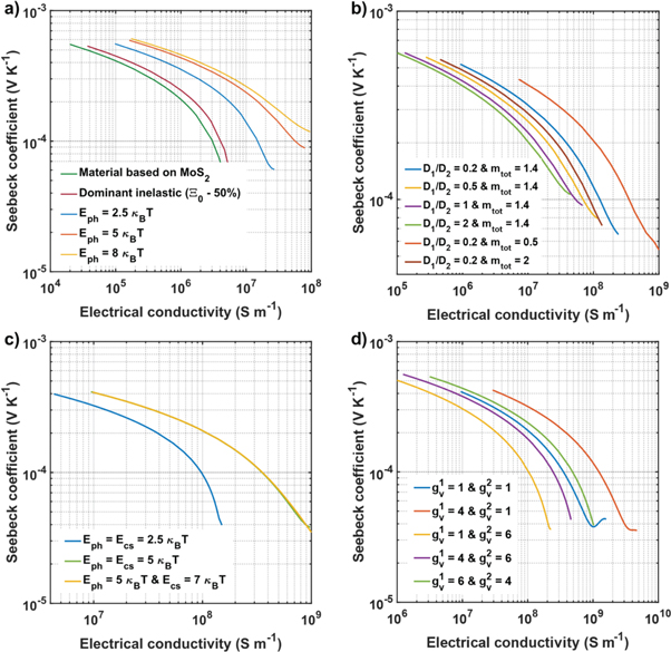
Figure 2. Material features identified in this study that can improve the power factor and their effect on power factor. (a) Effect of inelastic dominant material and the corresponding phonon energy (Eph) on power factor enhancement. (b) Power factor is calculated by changing the total DOS and relative height difference (D1/D2) in DOS of valleys. (c) Matching the valley splitting (Ecs) and phonon energy (Eph) to 5 kBT maximizes the power factor along with the Fermi window utilization. (d) Valley degeneracy ( ) and its effect on power factor of the material. Higher degeneracy in the main valleys maximizes the power factor.
Download figure:
Standard image High-resolution imageOur approach tries to create a rectangular shape for the product of relaxation time (τn) and DOS (Dn) using the step-like DOS. The valley splitting (Ecs) controls the width of first step, which in turn decides the width of TDF. We already know that the ideal shift in the onset of scattering occurs when Eph = 5 kBT. Now by further matching this with the width of the first step (when Ecs = Eph), transport can be effectively restricted to first step or valley. By calculating the power factor in a 2D material in which inelastic scattering is dominant with D1/D2 = 0.2 and mtot = 0.5 when varying the valley splitting, a maximum is observed when Ecs = Eph = 5 kBT as shown in figure 2(c). Further increase in Ecs beyond 5 kBT while limiting Eph to 5 kBT, does not help since the width is limited by Eph. Till now, we studied the effect of different material parameters on power factor assuming the degeneracy of the valleys to be 1 (circular valleys). Now to study the effect of valley degeneracy,  is varied but D1/D2 is still maintained at 0.2 by adjusting the
  . As shown in figure 2(d), high valley degeneracy for D1 (the valley that contributes to transport the most) improves the power factor. However, a higher degeneracy for the secondary valley deteriorates σ, thereby reducing the power factor. This is due to the availability of more states in the second (satellite) valley to scatter into from the first valley. A related strategy of increasing band degeneracy by valley alignment was studied to demonstrate an improvement in the power factor of half-Heusler alloys, showing that including intervalley processes is critical in obtaining accurate results [37]. While our approach also relies on inelastic scattering, we observe largest improvements when both intervalley and optical phonon emission are aligned (Eph = Ecs).
Figure 3(a) shows the step-by-step contribution towards Seebeck coefficient and electrical conductivity from each material selection criteria proposed here that can be achieved or maximum achievable power factor enhancement. The power factor gains seen by introducing these selection criteria and the influence of carrier concentration is shown in figure 3(b). The dominance of inelastic processes along with the optimal optical phonon energies provide at least ten-fold increase in power factor. A low D1/D2 along with low effective mass gives a further six-fold increase in power factor. Implementing the rest of the proposed selection criteria can boost the overall power factor by two orders in magnitude. Finally, to understand the correlation between TDF and the power factor achieved, TDF is plotted in figure 3(c) for each of the identified selection criteria. The progression in figure 3(c) shows that implementing these selection criteria results in narrowing transport bandwidth, with increasing proportion of transport contributed by states between the bottom of the conduction band and 5 kBT (0.13 eV at room temperature), corresponding to increases in power factor. To compare the material selection criteria with already defined metrics, SF is calculated while introducing the features identified in this study (as shown in figure 3(d)). The value of the SF is calculated by finding a cut-off energy E* that maximized the  consequently, the SF is independent of carrier concentration. Comparing the SF values (y-axis in figure 3(d)) with our calculated power factors (x-axis), shows the inability of SF to predict the power factor enhancement seen here. In 2D systems, the SF can be approximately reduced to D2/(D1 + D2) due to their step-like DOS. Since SF is only controlled by the asymmetry in the DOS, it is not able to completely capture the changes that occur in the TDF, primarily those related to inelastic scattering. Instead, SF is only affected by D1/D2 and increases when D1/D2 is reduced. Using only SF as a selection criterion will result in a broad spectrum of 2D materials due to their intrinsic step-like DOS. Hence there is a need to look beyond SF for the features like the ones identified in this study, that can be used as material selection rules for 2D materials for better power factor prediction.

Figure 3. (a) Material selection criteria (differentiated by the color) identified in this study, their effect on Seebeck coefficient and electrical conductivity. (b) The power factor enhancement achievable by introducing these material selection criteria at different carrier densities. By introducing these features there is a two-orders-of-magnitude improvement in the power factor of MoS2. This shows that any highly degenerate 2D material with high effective mass, low D1/D2 and valley splitting of 5 kBT improves power factor. Power factor will be further boosted if scattering is predominantly by inelastic processes with phonon energies of 5 kBT. be just(c) Corresponding transport distribution function (TDF) at different material selection criteria shows that improving TDF improves power factor. (d) Shape factor is calculated for the material features identified in this study to show the power factor enhancement achievable that is not reflected in the shape factor. Note: the color of each curve represents the corresponding selection criteria as labeled in (a) and all the simulations are performed at T = 300 K.
Download figure:
Standard image High-resolution image
Using the simple transport model as described here along with the recent development of 2D databases [47] that are comprehensive, identifying higher power factor materials could be done at a faster pace, especially if materials databases add transport properties such as deformation potentials, which can be obtained from first principles calculations. To corroborate the trends we predict, we contrast two popular TMDCs, MoS2 and WSe2. Experimental observations showed a larger power factor MoS2 (around 8.5 mW m−1 K−2) [51] than in WSe2 (3.2–3.7 mW m−1 K−2) [52]. Using the selection criteria proposed here and properties calculated from first principles, we can predict this decrease in WSe2, even though the two have similar electronic bandstructure [53]. With small valley separation of 16 meV in WSe2 versus 70 meV in MoS2, coupled with smaller optical phonon energies (28.5 versus 47 meV) hurts the power factor despite low elastic scattering (due to lower acoustic deformation potential) and smaller effective mass of WSe2 [53]. While our model produces higher power factors (44 and 6 mW m−1 K−2 for MoS2 and WSe2, respectively) than what was measured, mainly due the presence of impurities in the experiments, the relative ordering is reproduced correctly.
In conclusion, the search for new highly efficient TE materials requires that we identify candidates that have a high power factor. Here, a novel approach is proposed to ease the process of this material search by identifying those materials properties that ensure high power factor. A simple numerical model based on the widely-used effective mass approximation is implemented; the model captures inelastic scattering in 2D semiconducting materials with step-like DOS. We find that inelastic processes delay the onset of scattering, thereby maximizing the utilization of the Fermi window for transport. Our simulations show that materials where inelastic processes are dominant (or elastic processes are suppressed), specifically when optical phonon energy Eph equals 5 kBT, improve the power factor. A further enhancement is possible if the separation between the DOS of valleys is large (lower D1/D2), the effective mass is low, and the conduction-band valley that participate in transport have high degeneracy. By introducing this combination of material features in our prototype material, based initially on MoS2 for comparison, the power factor is boosted from 0.044 Wm−1 K−2 in MoS2 to 22 Wm−1 K−2 in a hypothetical material that has all of the aforementioned features, which is an increase of more than two orders in magnitude. We believe the material selection rules formulated here can help researchers to reduce the time and resources in the process of predicting and preselecting 2D materials that have high power factor.