

Abstract
In this work, we investigate polycrystalline Ni and FeGa magnetostrictive microstructures on pre-poled (011)-cut single crystal [Pb(Mg1/3Nb2/3)O3]1−x-[PbTiO3]x (PMN-PT, x ≈ 0.31) with linear strain profile versus applied electric field. Magnetostrictive microstructure arrays with various geometries are patterned on PMN-PT. Functionalized magnetic beads are trapped by localized stray fields originating from the microstructures. With an applied electric field, the magnetic domains are actuated, inducing the motion of the coupled particles with sub-micrometer precision. This work shows promise of using energy-efficient electric-field-controlled magnetostrictive micro- and nanostructures for manipulating magnetic beads via a linear strain response. The work also demonstrates the viability of cells suspended in solution on these structures when subject to applied electric fields, proving the cytocompatibility of the platform for live cell sorting applications.
Export citation and abstract BibTeX RIS
1. Introduction
The continuously increasing interest in nanoscale magnetic devices has encouraged researchers to develop new methods of controlling magnetism at the nanoscale. One such method involves artificial multiferroic heterostructures, where strain induced in piezoelectric materials is transferred to a magnetoelastic material layer to enable control of magnetism via an electric field. Compared to conventional electric current-control of magnetism, electric-field-driven control of magnetism in multiferroic heterostructures has several advantages. For example, the multiferroic approach allows for reduction of power dissipation in small scale applications, and the accompanying potential for highly arrayed and localized device actuation. This multimodal control holds promise in the development of new energy-efficient applications, including nonvolatile memory devices [1, 2], actuators and transducers [3], and miniature antennae [4]. Furthermore, the potential of electric-field-controlled magnetism in biomedical applications has been explored in the manipulation of magnetic particles [5]. Recently, manipulating magnetic particles with local magnetic fields has emerged as an appealing method for transporting bio-particles labeled with these magnetic beads [6, 7]. While extended exposure to dielectrophoretic traps [8] or optical tweezers [9] could damage cells, transport and trapping via magnetic particle manipulation is a nondestructive alternative. In addition, magnetic particle affinity to particular proteins, introduced through antibodies or other recognition elements conjugated to the particle surface, provides cell-type specificity to manipulations.
While using localized magnetic forces for manipulating magnetic microbead motion (e.g. magnetic tweezers [10]) allows remote control, the prevalent approaches for controlling the movement of magnetic beads along with bound bio-particles are not capable of operating with a large array of individually addressable elements. Previous approaches involve either external rotating magnetic fields or microfabricated electromagnets, with the former being bulky and de-localized [5] and the latter posing problems such as on-chip heating [11]. On the other hand, using an electric field to control magnetic domain motion arises as a viable solution which not only benefits from magnetic force control with high precision, but also avoids problems such as joule heating and the need for bulky external magnets.
Moreover, it is of paramount importance to separate and manipulate cells and other bio-particles individually and in parallel for rapid biological analyses [12, 13]. By employing magnetic domain walls whose motion is tunable via electric-field using multiferroic heterostructures and combining the device with microfluidics, 'lab-on-chip' devices can be developed that are capable of controlling the movement of detected entities with high precision, for downstream sorting, sequential reaction, and analysis. Controlling the coupling of the beads to the domain wall movement along with parallel optical imaging and analysis technologies [14] opens up opportunities to a myriad of applications for rapid cell analysis in sorting based on complex phenotypes [15]. Large arrays of individually addressable cells are particularly important for sorting rare cells in a population that may be useful diagnostically (e.g. antigen-specific T-cells, circulating tumor cells, etc) or for selecting rare clones with useful properties for cell therapies or cell-based bio-manufacturing.
[Pb(Mg1/3Nb2/3)O3]1−x-[PbTiO3]x (PMN-PT) is one of the most commonly used ferroelectrics in such multiferroic heterostructures. PMN-PT with composition close to the phase boundary (x ≈ 0.32–0.34) will undergo a morphotropic phase transformation [16, 17] with giant electromechanical response. Sohn et al [5] have previously demonstrated strain-mediated deterministic domain wall motion in Ni rings on single crystal (011) [Pb(Mg1/3Nb2/3)O3]1−x-[PbTiO3]x (PMN-PT, x ≈ 0.34) with morphotropic phase transformation, which induces a large hysteretic strain jump at an electric field of ∼0.5 MV m−1. Such strain change induces domain motion in the ring structures, which subsequently results in abrupt particle motion. Magnetoelectric Ni/(011) PMN-PT heterostructures with different compositions have been extensively researched [18–22] with magnetization reorientation controllable by electric-field, providing the groundwork for further optimization and applications. While Ni (λs(Ni) = −33 × 10−6) has been a popular choice for the ferromagnetic component in these systems, FeGa with an order of magnitude higher magnetostriction (λs(FeGa) = 350 × 10−6) is attracting more attention due to the potential enhanced magnetoelectric coupling figure of merit applicable to a broad range of uses, such as being a promising candidate for memory devices [2].
In this work, we describe the fabrication process for magnetostrictive Ni and FeGa microstructures on piezoelectric PMN-PT. We chose Ni because it has been widely investigated in multiferroic systems in spite of the fact that it possesses only a moderate magnetostriction coefficient. We also include results on FeGa because its higher magnetostriction coefficient enables greater control of its magnetic state. We then demonstrate tuning of the magnetic state of nanoscale structures using electric fields, as shown by x-ray microscopy. The device behavior was also examined with nanoscale superparamagnetic beads, and the electric-field-driven steady speed bead motion with response to the linear strain variation was captured by a high-speed camera.
Compared to the work of Sohn et al [5] using PMN-PT with morphotropic strain transformation, this work features PMN-PT with a linear strain. The benefit of actuating the particle movement using PMN-PT with linear strain is that it allows us to operate in a regime where the particle displacement is proportional to the applied electric field. The domain motion is activated at a comparable smaller strain with the applied field in the range of 0.16–0.32 MV m−1. While recent work has demonstrated the inhomogeneous nature of strain distribution in the single crystal PMN-PT [18], this response of the bead's continuous rotational behavior along the perimeter of the ring corresponds well to the linear macrostrain profile of the [Pb(Mg1/3Nb2/3)O3]0.69-[PbTiO3]0.31. Localized capture of single particles with nm to μm diameters at the onion state domain wall of Ni and FeGa rings, and at the corners of squares with partial closure domain are observed by optical and fluorescence microscopy [23]. The advantage of using these microstructures with localized domains is to enable single particle capture at specific locations rather than agglomerates of beads. In addition, a successful attempt to settle cells to the surface of the device were demonstrated, and cell viability under applied electric field from 0 to 0.8 MV m−1 was confirmed.
2. Experimental methods
2.1. Fabrication of microstructures on piezoelectric substrate and magnetization state initialization
The multiferroic heterostructure consists of a (011) cut [Pb(Mg1/3Nb2/3)O3]1−x-[PbTiO3]x (PMN-PT, x ≈ 0.31) single crystal substrate (Atom Optics Co., Ltd, Shanghai, China). The piezoelectric coupling coefficient d33 of the substrates is between 800–1200 pC/N when poled in the [011] direction, and the d31 is −410 pC/N. 5 nm Ti and 50 nm Pt thin films are deposited on both sides of the 1 cm × 1 cm × 500 μm thick substrate as electrodes to actuate the substrate in a parallel plate capacitor geometry. Electron beam lithography defines sub-micron features in PMMA A2 resist onto the Ti/Pt surface. Prior to deposition, the PMN-PT is electrically pre-poled in the out-of-plane direction with an electric field of 0.4 MV m−1. A 5 nm Ti adhesion layer and a 15 nm polycrystalline Ni layer were deposited by e-beam evaporation using a CHA Solution electron beam evaporator, with a deposition rate of 0.3 Å s−1. FeGa (20 nm) was deposited via magnetron sputtering using an Ulvac JSP 8000 (base pressure less than 4 E-7 Torr) at 100 W and a sputtering pressure of 1.0 mTorr. Films were then patterned by a lift-off process, leaving a continuous Ti/Pt layer covering the PMN-PT substrate and sub-micron magnetic features defined on top of this metal layer.
Prior to applying an electric field through the substrate, magnetization states in the ring and square microstructures are initialized by applying and subsequently removing an in-plane external magnetic field (Hinit) of 0.5 T. The magnetic field is applied in the direction bisecting the directions of the principal strain axes, [100] and [01-1] of the PMN-PT substrate. After the removal of Hinit, the rings of interest will form 'onion states' [5, 24–26] with the two onion state domains aligned along the direction of Hinit, as a result of competition between exchange energy and demagnetization energy. Depending on the aspect ratio between the ring width and ring diameter, the stabilized onion state has two forms of domain walls: transverse or vortex [5]. On the other hand, the microsquares will fall into a full Landau state, or a partial Landau state due to physical imperfections [18, 27, 28]. The direction of Hinit is so chosen in order to allow a 45° deterministic rotation of the initialized magnetic state, once the electric field is applied to the substrate [5, 18]. A schematic of the sample with its setup is shown in figure 1.

Figure 1. Schematic of the sample and the relative orientations between the initial field direction and the PMN-PT principal strain axes. After the initialization field, Hinit, is removed, an electric field is applied through the thickness of the ferroelectric PMN-PT via the top and bottom electrodes made of Pt thin films, inducing a differential in-plane strain.
Download figure:
Standard image High-resolution image2.2. XMCD-PEEM for magnetic domain imaging
X-ray magnetic circular dichroism-photoemission electron microscopy (XMCD-PEEM) at beamline 11.0.1.1 of the Advanced Light Source of the Lawrence Berkeley National Laboratory is used to image the magnetization contrast in our magnetic structures. Apart from high resolution imaging, other advantages of XMCD-PEEM include element-specificity and non-invasiveness during electric-field sweeps [29]. For this study, XMCD-PEEM is mainly used to characterize the initialized magnetization states in the Ni and FeGa microstructures of different dimensions on PMN-PT at room temperature.
2.3. Nanomagnetic particle preparation
Superparamagnetic (SPM) beads with diameter of 0.6 μm and 2 μm (Spherotech, Libertyville, IL) are suspended in distilled water in a 1.5 ml eppendorf tube. The surface of the superparamagnetic microbeads is functionalized with streptavidin to enable bioconjugation for future cell applications.
As shown by this part of the study, using the micro- and nanoscale SPM beads is a powerful method to detect the location of the domain walls on a magnetostrictive microstructure based on the magnetic stray field emanating from it. When methods such as XMCD-PEEM are not easily accessible, this alternative method provides a lab-based tool to image the magnetic domain wall distribution in a straightforward manner. With fluorescent beads, this method allows for imaging with a large field of view where, in this case, arrays of microstructures can be imaged simultaneously. Figure 2 shows the normalized magnetic hysteresis loop of the SPM beads 0.6 μm in diameter, measured by superconducting quantum interference device (SQUID) magnetometry (Quantum Design MPMS 3). For preparation, a drop of beads suspended in the solution was dried on a plastic chip prior to the SQUID measurement.
2.4. Trapping of superparamagnetic beads by stray field from Ni and FeGa microstructures
Nanomagnetic particles provide a simple detection method of the magnetic stray field of microstructures. The surface of the nanoparticles is functionalized by different chemical groups to react with specific biological elements. In contrast to conventional methods to detect magnetic domain wall at the nanoscale such with XMCD-PEEM or magnetic force microscopy (MFM), this technique is highly accessible, non-invasive and compatible with in vitro downstream applications.
SPM sub-micron sized beads were introduced to the patterned sample after passivating the surface with pluronic F-127 to prevent non-specific interactions. The beads were allowed to settle and sediment to the sample surface. Non-magnetically attached SPM beads (i.e., non-specific adhesion) were washed off with low flow rates. In the experiments with electric-field induced strain in the PMN-PT, the SPM solution is applied at the center of the sample surface.
2.5. Electric-field-driven particle motion
Samples were initialized in an electromagnet and then mounted on a custom chip carrier, after which a droplet of fluid containing SPM beads was placed on the sample surface. Sedimentation and trapping of beads at magnetic domain walls was observed. Upon confirmation of the bead capture, the voltage was increased in steps of 40 V from 0 to 200 V, corresponding to a 0.0–0.4 MV m−1 electric field within the piezoelectric PMN-PT substrate. When an electric field is applied to the substrate, the induced strain will alter the magnetic energy landscape, which determines the preferential magnetization direction in either the Ni or FeGa. When a sufficient strain is applied, the magnetization states in both magnetostrictive materials will be modified. Since the magnetostriction coefficients, λs, of Ni and FeGa have opposite signs, the easy axis in Ni will be reoriented towards the compressive strain direction [100], while the easy axis in FeGa will be reoriented towards the tensile strain direction [01-1] of (011)-cut PMN-PT.
2.6. Optical microscope and Fluorescent microscope imaging and data analysis
The device was viewed using an inverted microscope Nikon Ti-U (Nikon, Melville, NY) illuminated by a mercury arc lamp with 40× and 100× objectives. Fluorescent SPM nanobeads captured on a magnetic array were imaged with a CCD Coolsnap HQ2 camera (Roper Scientific, Evry, France). Images were processed by NIS Elements software (NIS-Elements Package Ver. 4.00, Nikon) to locate in high resolution the trapping location on the domain wall. High-speed videos of microstructures to capture Brownian motion and electric-field-driven motion experiments were recorded using a Fastec IL3 high-speed camera at 1000 frames per second under bright field illumination.
2.7. Microfluidics integration
A PDMS device was fabricated with standard soft-photolithography to form a channel (H = 100 μm, W = 0.5 cm, L = 0.5 cm), as shown in figure 2. The master wafer was patterned with KMPR 1050 (Microchem Corp., Woburn, MA, USA). PDMS (Sylgard 184, Dow Corning, Midland, MI, USA) was mixed with a curing agent at a 10:1 weight ratio. The mixture was poured onto the master wafer and degassed to remove air bubbles. The PDMS was cured at 100 °C overnight. Microchannel devices were cut out and aligned on the surface of Ni/(001)-PMN-PT and FeGa/(001)-PMN-PT multiferroic heterostructures after an inlet and outlet were punched connecting to upstream and downstream portions of the channel. The bonded microchannels are capable of steering the flow and perform washing steps to test multiple SPM bead trapping events on the same device. Figure 3 shows the integration of the microfluidic chip on the surface of the magnetoelectric device.

Figure 2. Magnetization hysteresis loop measured by SQUID magnetometry for a suspension of the superparamagnetic nanobeads (∼600 nm in diameter) used for the fluorescent imaging.
Download figure:
Standard image High-resolution image
Figure 3. Microfluidic chip integrated on the top surface of the magnetoelectric device. Arrays of magnetostrictive micropatterns are located at the center of the device, viewed by optical microscopy.
Download figure:
Standard image High-resolution image2.8. Cell viability test
Jurkat leukemia cells (ATCC, Manassas, VA) were grown in RPMI 1640 media containing 10% fetal bovine serum (Invitrogen, Carlsbad, CA). Cells are cultured at 37 °C in a humidified atmosphere of 5% CO2. Cell viability is determined by Calcein AM green fluorescence stain (Thermo Fisher, Waltham, MA).
3. Results and discussion
3.1. XMCD-PEEM imaging of the microstructure arrays and localized fluorescent bead trapping
Upon removal of the initializing magnetic field (Hinit), Ni and FeGa rings relaxed into onion state domains while squares relaxed into Landau states due to energy minimization between exchange and demagnetization contributions. XMCD-PEEM characterized the domain configuration in the microstructures by spatially resolving the magnetization contrast, where black and white indicate the magnetic orientation pointing to the right (0°) or to the left (180°), respectively, in the figures below.
Figure 4(a) displays the XMCD-PEEM images of Ni microstructures at initialization, showing onion states in rings. Fluorescent SPM micro- and nanobeads are used to pinpoint the location of the onion state domain walls, which are local sources of magnetic stray field, and bead trapping locations using the same magnetic initialization protocol as used for the XMCD-PEEM samples. As an overlay of bright field and fluorescent microscope images, figure 4(b) presents arrays of Ni rings of outer diameters 2 μm–6 μm capture fluorescent beads at the DWs location of the onion state. A series of time-lapse images of an array of Ni rings with OD of 4 μm, and w of 350 nm capturing beads is shown in figure 4(c).
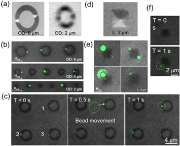
Figure 4. Fluorescent beads of 0.6 μm (green) trapped and localized on the magnetic domain walls of the Ni microstructures. (a) XMCD-PEEM images of Ni rings. (b) Overlay of bright field and fluorescent microscope images of fluorescent beads coupled to rings of 6 μm, 4 μm, and 2 μm in diameter. (c) Time-lapse images of 4 um Ni rings capturing fluorescent bead (0.6 μm in diameter) in the microfluidic channel, corresponding to the location of the DWs of Ni rings, as shown in the PEEM images. (d) XMCD-PEEM images of Ni squares with 2 μm in length. (e) Overlay of bright field and fluorescent microscope images of fluorescent beads captures at the corners of 2 μm squares. (f) Time-lapse images of FeGa squares of 2 μm in length capturing fluorescent bead at the corner. Dashed circle highlighted the position of the fluorescent bead.
Download figure:
Standard image High-resolution imageFigure 3(d) shows the XMCD-PEEM images of Ni square forming a Landau flux-closure state with four triangular domains (magnetic vortex state [18]). Although the Landau state forms to minimize the demagnetization energy, the magnetization at the center of such vortex state points out of the plane to avoid drastic increase in exchange energy. Both Hall micromagnetometry and micromagnetics simulation studies on Landau state by Breitenstein et al [30] suggested that the z-component of the stray field from the vortex core with a few nm in size becomes completely masked by the stray field from the domain walls from the four triangular domains at around 90 nm in their permalloy squares of 2 μm in length and 20 nm in thickness. This helps to explain that with magnetic particles with diameter more than 0.5 μm, the trapping by the vortex core with only a few nanometers in diameter and limited z-direction stray field range was not observed. Instead, consistent trappings occur at multiple corners of the squares (see figure 4(e)), indicating the partial flux-closure domain state produces high stray fields at the corners. Furthermore, according to a recent XMCD-PEEM study based on Ni microsquares on PMN-PT [18], the squares do not always form 'perfect' flux-closure Landau state (see figure 4(d)). Figure 4(f) shows the time-lapse images of a square of 2 μm in length capturing a bead at the corner. Combined with the bead trapping experiment, it can be observed that the initialized magnetic vortex state produces strong stray field at the corners of the squares. Such partial closure domain occurs due to several reasons: (1) physical imperfections of the fabricated micron scale structure with 15–20 nm in thickness, and (2) initial non-uniform magnetic uniaxial anisotropy could also contribute to the deviation from a perfect Landau state.
When no flow is applied and particles are simply allowed to sediment, high-speed camera footage of the trapping event shows that motion stops quickly upon interaction of the particle with the domain wall of a Ni ring (see supplementary video 1 is available online at stacks.iop.org/MFM/1/014004/mmedia), confirming the strong magnetic interaction between the bead at the domain wall that has sufficient energy to overcome thermal energy. In particular, prior to the moment of capture, the particle moves randomly (see figure 5), suggesting that the observed motion is from Brownian diffusion and/or environmental vibration. The sudden decrease of the amplitude of this motion upon encountering the domain wall and its failure to reoccur thereafter must be from a localized pinning potential the particle experiences, in this case due to the magnetic field gradient from the domain wall.

Figure 5. (a) Representative particle trapping event in the absence of flow (1 μm particle, 4 μm diameter ring. Left: particle path overlaid on image of 4 μm Ni ring. (b) Particle displacement relative to position at time 0 (Euclidean distance) vs time over the course of the trapping event. Trapping occurs around 1.5 s and most random motion ceases.
Download figure:
Standard image High-resolution imageTo investigate whether higher magnetostrictive FeGa microstructures follow similar paradigm of Ni microstructures, microstructures of similar dimensions are also examined. Figure 6(a) shows the XMCD-PEEM images of individual FeGa rings with outer diameters (OD) of 6 μm, 4 μm, and 2 μm, and widths (w) of 300 nm, 350 nm and 300 nm, respectively. With the desired onion states confirmed by XMCD-PEEM, fluorescent SPM micro- and nanobeads are used to confirm the one-to-one correspondence between the location of the onion state domains (see figure 6(b)). For FeGa squares of 2 μm in length, the beads are observed to be trapped on the corners, as shown in figure 6(c). Figure 7 shows the time-lapse images of an array of FeGa rings capturing beads, along with the process of bead capturing by the rightmost No. 3 ring. The three rings shown here have a diameter of 2 μm and width of 300 nm.

Figure 6. (a) Initialized onion states in polycrystalline FeGa rings of varied width and diameter, with a thickness of 20 nm, observed by XMCD-PEEM. (b) Rings of various sizes in (a) trapping fluorescent nanoparticles via the magnetic stray field emanating from the onion state domain. (c) Squares of 2 μm in length trapping fluorescent particles on the corners.
Download figure:
Standard image High-resolution image
Figure 7. Time-lapse images of 2 μm ring (No. 3) capturing a fluorescent bead in the microfluidic channel, corresponding to the location of the DWs of FeGa rings, as shown in the PEEM images. Ring No. 1 and No. 2 have captured beads prior to No. 3. All the three rings trapped beads locally along the x direction, in which Hinit was applied.
Download figure:
Standard image High-resolution image3.2. Strain profile characterization
Previously, Sohn et al [5] demonstrated the morphotropic transformation when PMN-PT transitioned from rhombohedral to orthorhombic in (011)-cut PMN-PT, inducing a large, nonlinear strain jump to the substrate at 0.5 MV m−1 [5]. The transformation initiated abrupt particle motion to a full 45° rotation instantaneously. This study focuses on a PMN-PT with a different composition, resulting in a linear strain profile with electric field, as shown in figure 8. The strain profile was measured by attaching a biaxial strain gauge onto the surface of the sample. As we apply electric field of various magnitudes, the induced strain will result in a change in the electrical resistance that is proportional to the strain magnitude. With a linear strain profile, we expect a smoother modulation of the magnetic particle position along the perimeter of the ring as the electric field is applied across the substrate.

Figure 8. (a) Magnetoelectric device is mounted on a leadless chip carrier (LCC), and a biaxial strain gauge is mounted on the surface of the device for strain profile characterization. (b) Linear strain response along the [01-1] and [100] directions of the PMN-PT substrate to the applied electric-field is measured using the strain gauge.
Download figure:
Standard image High-resolution image3.3. Electric-field-driven particle displacement
Though electronically actuated particle motion in multiferroic heterostructures like these has been demonstrated previously using PMN-PT substrates with a nonlinear strain response [5], actuation using linear strain response is more desirable due to the potential for controllable, continuous particle motion. Due to the linear strain, within a certain range of applied fields the particle displacement is also expected to be proportional with respect to the electric field. However, as the magnitude of the strain response is lower in these linear strain samples, it was necessary to demonstrate that actuation of domain wall motion is still possible at nondestructive electric field strength. To this end, stepwise voltage was applied to PMN-PT substrate with Ni microstructures after particle trapping. (See supplementary video 2).
Successful, electrically driven continuous particle motion was observed for particles trapped on Ni rings, wherein a trapped magnetic particle rotated through several intermediate angles as the applied voltage was increased until aligned with the compressive strain axis [100] of the PMN-PT substrate (see figure 9). No other motion of the trapped particles during this process was observed, including any reoccurrence of the random diffusive motion described above, suggesting that the particles remain trapped during the domain wall motion. This distinguishes these motions from the large, nonlinear strain-mediated displacements observed in Sohn et al [5], in which the particles were moved in one step or even ejected from the domain wall due to the sudden DW rotation.

Figure 9. Continuous magnetic bead movement, driven by applied electric field to the PMN-PT with linear strain response, along the perimeter of the Ni ring, 4 μm in diameter and 600 nm in width, captured by optical microscope. The diameter of the bead is 1 μm.
Download figure:
Standard image High-resolution imageInterestingly, however, magnetic beads trapped at the corners of the squares of 2 μm, either in Ni or FeGa, remain stationary after the application of electric field, with an example of a Ni square shown in figure 10. Lo Conte et al [18] has recently reported more details of electrical-field induced domain state change in Ni 2 μm squares. One explanation is that as the magnetic vortex state (figure 10(a) left) becomes a two-domain state whose domain wall aligns with the compressive strain axis in [100], the high energy density of the magnetic stray field still exists at the diagonal corners of the square. Taking into account the non-uniformly distributed strain in the substrate and imperfections from fabrication, the domain wall of the two-domain state does not always overlap perfectly with the diagonal of the square, leading to the locations of the bead trapping laying slightly away from the corner of the square. However, compared to the particle motion with respect to the ring, the particle captured by the corner of the square stabilizes at the same location. The different responses of magnetic particles to the two different geometries of the microstructures suggest a way to pattern various microstructures on the same device with different degrees of freedom for strain-mediated particle control, when compared to micropatterned magnetic arrays without such multiferroic control.
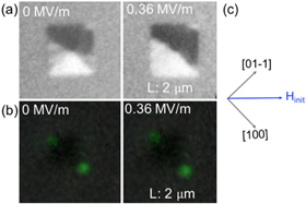
Figure 10. (a) XMCD-PEEM images of a Ni square with a magnetic vortex state at zero electric field, and evolves into a two-domain state at 0.36 MV m−1, (b) a Ni square of 2 μm in length trapping fluorescent beads on the corners before and after applying voltage and (c) Sample orientation with respect to the initialization magnetic field direction.
Download figure:
Standard image High-resolution image3.4. Cell viability on magnetoelectric devices
To investigate the cell viability [31] on the magnetoelectric devices with applied electric fields up to 0.8 MV m−1, live Jurkat cells are stained with Calcein AM green fluorescent dye. Cell membrane damage causes the green dye to escape, indicating cell death. Stained cells were settled on the Pt electrode covering the PMN-PT substrate. Cells remained viable when voltage was applied up to 400 V, corresponding to an electric field of 0.8 MV m−1 (figure 11). This indicates cytocompatibility of the platform for in vitro cell biomedical applications while actuating a magnetoelectric device with adequate packaging. (See supplementary video 3 & 4).

Figure 11. Viability test on multiferroic heterostructure platform using Calcein AM stain (a) stained viable cells, (b) stain leakage of damaged cells, (c) before applying voltage and (d) after ramping up the voltage to 400 V applied to the top and bottom electrodes, with corresponding electric field up to 0.8 MV m−1, the cells are viable for downstream bio-applications.
Download figure:
Standard image High-resolution image
4. Conclusions
In summary, we have demonstrated the trapping of sub-micron magnetic particles by magnetostrictive Ni and FeGa microstructures at specific locations, including onion state domain wall of the ring structures, and partial flux-closure domain at the corner of squares. XMCD-PEEM shows the magnetic domains in both Ni and FeGa microstructures, while optical and fluorescent microscope captures how the beads interact with the domain walls, highlighting an alternative nondestructive method of indirectly visualizing the domain wall locations in these magnetostrictive microstructures. The linear strain response when electric field is applied through the thickness of the PMN-PT substrate enables a steady and continuous translational movement of the magnetic bead to the newly electrically introduced magnetic easy axis. The cytocompatible device provides a promising pathway to develop multiplex particle and cell manipulation platforms with sub-micron precision.
Acknowledgments
We acknowledge the use of fabrication facility at the Integrated Systems Nanofabrication Cleanroom at the California Nanosystems Institute. This work was supported by the NSF Nanosystems Engineering Research Center for Translational Applications of Nanoscale Multiferroic Systems (TANMS) under the Cooperative Agreement Award (EEC-1160504). The work at the Advanced Light Source at Lawrence Berkeley National Laboratory is supported by the Director, Office of Science, Office of Basic Energy Sciences, U S Department of Energy, under contract number DE-AC02- 05CH11231. Additional work was supported by NSF EFRI NewLaw, award No. 1641128.