
Abstract
The growth rate of crystalline GaSe from solution was increased by using indium as a solvent. The solubility and concentration gradient of Se were measured using differential scanning calorimetry (DSC). The Se solubility and the temperature coefficient of the solubility were respectively 15 times and 2.2 times greater in crystals grown from an In flux with GaSe at saturation compared with the case of Se dissolved in a Ga flux. In this study, we succeeded in growing InxGa1−xSe ingots from an In flux without the need for a seed crystal, and in increasing the growth rate of GaSe from solution. In addition, we used difference frequency generation to generate THz waves (with a frequency of 9.7 THz) in an InxGa1−xSe mixed crystal and investigated the relationship between the output energy of the THz radiation and the interaction length of the excitation light. The conversion efficiency of THz wave (9.7 THz) from the InxGa1−xSe mixed crystal with thickness of 860 μm was 26 times greater than that of GaSe crystal with thickness 100 μm grown from Ga solvent.
Export citation and abstract BibTeX RIS

Original content from this work may be used under the terms of the Creative Commons Attribution 4.0 licence. Any further distribution of this work must maintain attribution to the author(s) and the title of the work, journal citation and DOI.
1. Introduction
Gallium Selenide (GaSe) is one of the most promising layered chalcogenide semiconductors for future novel semiconductor devices. There is a great deal of interest in the electrical and optical characteristics of 2 dimensional (2D) GaSe, which has a finite energy bandgap. The interlayer van der Waals bonding force of GaSe has been studied [1], as have its uses for spin-field-effect transistors [2] and as a THz wave light source [3].
Because it has an extremely asymmetric layered crystal structure, GaSe has a relatively high second order nonlinear optical (NLO) constant ( ) [4]. Therefore, THz waves can be generated from GaSe crystals via the difference frequency generation (DFG) process, which is a second order NLO effect. In addition, GaSe crystals are transparent over a wide range, from infrared (IR) to THz frequencies, and it is, theoretically, possible to use them to generate THz waves from sub-THz to mid-IR (0.1 ∼ 100 THz) frequencies via DFG [5]. Furthermore, because GaSe, which is a 2D layered semiconductor, has high birefringence, it is possible to apply collinear phase matching to generate THz waves via DFG, and improvements in the conversion efficiency are expected using DFG [6–8].
Commercially available GaSe crystals are grown from high temperature melts by the Bridgman growth method. However, Bridgman grown GaSe crystals have structural disorder. There are two mixed polytypes (γ and ε type) and thermal equilibrium point defects introduced by high temperature growth at the melting point of GaSe (938 °C) [9, 10]. In addition, since Se has a higher vapor pressure than Ga, the composition is non-stoichiometric due to dissociation of Se during crystal growth. These crystal-structural disorders and nonstoichiometric composition lead to a reduction in transparency in the IR & THz frequency ranges and reduce the conversion efficiency in the DFG process [11]. We succeeded in suppressing the THz absorption due to the nonstoichiometric composition by selectively growing single ε-type GaSe by the 'Temperature Difference Method under Controlled Vapor Pressure' (TDM-CVP) [12]. TDM-CVP enables fixed low temperature growth at temperatures 200 °C below the melting point of GaSe by having a temperature gradient in the Ga–Se solution. Furthermore, it is possible to control the stoichiometry of the GaSe crystal by controlling the Se vapor pressure applied to the Ga-Se solution during crystal growth [7]. Compared with GaSe crystals grown by the Bridgman method, the transparency of GaSe crystals grown by TDM-CVP are better in the near IR (λ = 1 μm) and high THz frequency ranges (>2.4 THz) [12]. In addition, the conversion efficiency using DFG in a GaSe crystal grown by TDM-CVP was  and this is greater than that obtained with Bridgman grown crystals, for which the conversion efficiency is
  [3].
[3].
However, the crystal size of GaSe grown by TDM-CVP is small (the thickness is about 300 μm) [7], because of the low solubility of Se in the Ga solvent [9] and the nucleation of multiple crystals. In collinear phase matching, the thicker the GaSe crystal is, the longer the interaction length of the excitation light [13]. Therefore, considering the absorption of the excitation light and the THz waves, it is expected that the power of THz waves generated using GaSe crystals can be enhanced by having the optimum thickness.
In order to increase the growth rate and thickness of GaSe crystals grown by solution growth, it is necessary to increase the Se solubility in the solution. The heterogeneous flux method is one method with which the solubility can be increased. There have been many reports of speeding up the growth rate by using a heterogeneous flux in the solution growth of GaN (Na flux [14]) and SiC (Cr, Ti, Fe flux [15–17]). In this work, we selected an In flux, in which it is easy to dissolve Ga and Se [18, 19].
It is expected that the crystal properties for generating THz waves can be improved by doping GaSe with In. Several studies have been done with the aim of improving the properties by doping GaSe with various elements such as S [20, 21], Te [22, 23], In, Al [24], Er [25], Ti [26], and Ge [27]. These reports of doped GaSe crystals are reviewed in [28]. In particular, doping the crystal with In increased the second-order NLO constant in second-harmonic generation (SHG) [29, 30] and the conversion efficiency for generating THz waves by DFG [31].
In this work, we investigated the solubility of GaSe and the Se content in an In flux at GaSe saturation by DSC. In addition, crystalline GaSe was grown from an In flux by the traveling heater method (THM). The indium content, optical transmittance and THz wave generation properties of crystals grown from an In flux were evaluated and compared with those of GaSe crystals grown from a Ga flux.
2. Solubility of Se in an In flux at GaSe saturation
2.1. Method
The solubility of GaSe in an In flux was evaluated by DSC (SDTQ600 TA Instruments Inc.). First, GaSe and In were inserted into an alumina cup with a lid. These were heated at 1073 ∼ 1103 K for 90 min until the GaSe was completely dissolved in the In. After heating, the temperature was reduced at 5 K min−1, and the temperature of the exothermic peak, which appears at segregation of the crystal, was measured at the saturated solution temperature. The above measurements were conducted in an Ar flow (200 ml min−1). Referring to the definition of the International Confederation for Thermal Analysis (ICTA), the temperature of segregation is defined by the intersection of the base line just before the peak and the tangent to the maximum slope of the rising peak. Additionally, we measured the solubility of GaSe in an In flux for many different GaSe:In ratios, and calculated the temperature coefficient of the solubility.
Table 1. The compositions of the In solutions and their segregation temperatures.
| Weight of In (mg) | Weight of GaSe (mg) | Se content in In flux at GaSe saturation (at%) | Temperature of segregation (K) |
|---|---|---|---|
| 65.3 | 7.3 | 4.0 | 812 |
| 51.1 | 12.5 | 7.9 | 857 |
| 49.8 | 30.3 | 16.0 | 934 |
| 41.6 | 39.3 | 21.1 | 982 |
| 30.6 | 54.1 | 28.9 | 1044 |
| 33.3 | 65.2 | 30.1 | 1054 |
2.2. Results
The compositions of the In solutions and their segregation temperatures are shown in table 1. Figure 1 shows the DSC spectra. As shown in figure 1, the GaSe is homogeneously dissolved in the In solution because there is only one exothermic peak in each cooling spectrum, which each has different Se content. There are 2 exotherms in the cooling spectrum of the In solution containing 4.0 at% Se. The reason for the exotherm near 875 K is that the cooling rate was changed from 10 K min−1 to 5 K min−1 at this temperature.
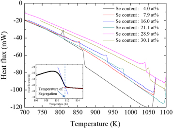
Figure 1. DSC spectra of In solutions with GaSe and (insert) the exothermic peak at segregation from the In solution containing 4.0 at% Se.
Download figure:
Standard image High-resolution imageFigure 2 shows the temperature dependence of the Se solubility in the In flux at GaSe saturation and in a Ga flux. The value of the Se content in the Ga flux was obtained from a plot of the Ga-Se system in [9]. As shown in figure 2, the solubility of Se in the In flux at GaSe saturation (30 at% @ 1054 K) is more than 15 times greater than that in the Ga flux (1.8 at% @ 1084 K). Furthermore, from linear approximation formulae, the temperature coefficient of the Se solubility in the In flux at GaSe saturation (0.1156 at%/K) is more than 2.5 times greater than that in the Ga flux (0.0458 at%/K). Therefore, because the solute diffuses faster with greater solubility and larger concentration gradient, the growth rate of GaSe from an In flux is expected to be faster.
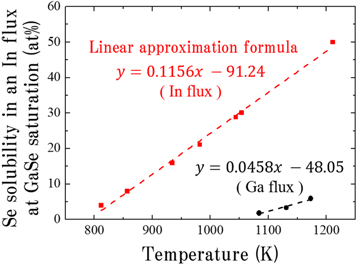
Figure 2. Temperature dependence of Se solubility in an In flux at GaSe saturation and in a Ga flux.
Download figure:
Standard image High-resolution image3. Crystal growth
3.1. Method
A schematic illustration of the equipment for crystal growth is shown in figure 3. In order to remove organic matter, the quartz ampoule and crucible were dipped in sulfuric acid/hydrogen peroxide mixture after washing with acetone. After the doping and washing, the quartz ampoule and crucible were baked at 450 °C at a pressure of 1 × 10⁻⁵ Torr for one hour. The source and flux material, granular gallium selenide (Kojundo Chemical Lab. Co., Ltd) and indium (DOWA Electronics Materials Co., Ltd), were inserted in the baked quartz crucible. The purity of the GaSe and the In were 3N and 6N, respectively. The size of a 1 gram shot of indium was 5 mm in diameter and 7 mm in length. The size of one grain of GaSe was 1–10 mm2 and its thickness was less than 1 mm. The amount of In and GaSe inserted in the growth crucible were 7.7 g and 20 g, respectively.

Figure 3. Schematic view of the equipment for crystal growth and the temperature distributions.
Download figure:
Standard image High-resolution imageIn order to orient the growth direction, a temperature gradient was applied, not only in the vertical direction but also in the horizontal direction, using a side sub-heater, as shown in figure 3. The temperature distribution shown in figure 3 was measured before inserting the growth vessel. In growing a layered crystal such as GaSe, the (001) plane grows along the direction with the largest temperature gradient [21]. The growth process is as follows. First, the growth vessel is fixed at the initial position shown by the solid red line in figure 3. At this position, homogenization and supersaturation occur in the In-Ga-Se solution by the diffusion of Ga and Se to the bottom of the crucible due to the temperature gradient. The growth vessel is kept in this initial position for 1 day. After homogenization, the growth vessel is mechanically lowered at a speed of 60 μm h−1 to the end growth position shown by the dashed blue line in figure 3. In figure 3, the highest temperature was 785 °C at depth of 51cm and the lowest temperature was 742 °C at depth of 55 cm. The ramp up rate to the growth temperature shown in figure 3 is 20 °C min−1 and the ramp down rate to room temperature is 1 °C min−1.
3.2. Results
Figure 4 shows an as-grown crystal grown from a Ga flux by temperature gradient solution growth and from an In flux by THM. As shown in figures 4(a) and (b), the crystal grown from the In flux is an ingot in the shape of the crucible, whereas the crystal grown from the Ga flux was plate-shaped [7]. In addition, the ingot was easily cleaved with a high quality (001) surface. The indices of cleaved plane were identified by the diffraction pattern of XRD measurement. This is the first time that a GaSe ingot has been grown from solution. According to the results of the DSC measurements, we consider that the increased growth rate is a result of an increase in the solute diffusion rate due to increases in the solubility and the temperature coefficient of the solubility. However, shadows in the transmission images, which seem to be fragments of solvent, were observed in some parts of the grown crystal. In order to evaluate the optical characteristics without the influence of that solvent, a 3 mm diameter aperture was used to limit observations to the clearer regions as shown in figure 4(b). The thickness of the crystal used for optical evaluations was 860 μm.
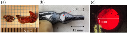
Figure 4. (a) GaSe crystal grown from a Ga flux (b) (001) cleaved ingot grown from an In flux (c) Optical transmission image of crystal attached to 3 mm diameter aperture.
Download figure:
Standard image High-resolution image4. Evaluation of the grown crystals
4.1. Methods
Electron probe micro-analyses (EPMA) with a JXA-8530F was used to measure the Ga, Se and In contents in the grown GaSe crystal. In this work, we used an undoped GaSe crystal grown by TDM-CVP [7] and an undoped InP wafer (Sumitomo electric industries, Ltd) as standard samples. The In content was measured at 7 points on a sample. We calculated the average and standard deviation of these 7 measurements.
In addition, we also estimated the indium content in the grown crystals from the lattice constant measured by XRD measurements, basing this estimate on the change in lattice constant due to indium doping. Symmetric x-ray diffraction patterns of InxGa1−xSe mixed crystals from (0 0 14) to (0 0 20) were measured by an automated multipurpose x-ray diffractometer (SmartLab, RIGAKU Ltd) with CuKα1 (λ = 0.154056 nm) radiation. The precise lattice constants were estimated by extrapolating to cos2 θ = 0 on a plot of cos2 θ versus the lattice constant c.
Visible to near infrared transmission spectra were measured by a UV/VIS/IR spectrometer V-570 (JASCO Inc., Japan). The spectral range was 500–2500 nm and measurements were made in 2 nm steps.
THz transmittance spectra were measured in the frequency range of 9–11 THz using a frequency tunable THz source. Figure 5 shows a schematic view of the experimental setup for the THz transmittance measurements. A near-infrared Nd:YAG laser (LOTIIS Inc.) with two channels was used to excite grating type Cr:Foresterite lasers. Because these lasers, which have gratings (1200 grooves/mm) for wavelength selection, achieve higher-frequency purity than prism type ones, the frequency purity of the generated THz waves is high as well as the excitation light. The wavelengths were 1203 nm and 1248 nm ∼ 1259 nm, respectively. The light from these lasers was mixed in a GaSe crystal under controlled phase matching conditions. The InxGa1−xSe mixed crystal was irradiated with THz waves generated in the GaSe crystal and the THz transmittance was measured. The diameter of the aperture in the aluminum in figure 5 is 3 mm. In order to make the surface of the samples flat, these were peeled using tape. The THz waves were detected by a 4 K-Si:Bolometer (Infrared Inc.). The NIR excitation light was safely removed by black polyethylene placed in front of the Si:Bolometer. The transmittance was calculated by dividing the voltage measured by the THz bolometer when the radiation passed through the sample by the voltage when no sample was installed. The absorption coefficient α was calculated using equation (1), where t is the thickness of the sample, T is the transmittance, and R = (n − 1)2/(n + 1)2 is the Fresnel power reflection coefficient [32].

THz waves were generated via difference frequency generation from the grown crystal. The optical system for generating the THz waves, as well as the THz transmittance measurement setup, is shown in figure 5. The GaSe crystal was replaced by the grown crystal. In this study, we generated 9.7 THz waves by eoo phase matching and compared the conversion efficiency with that for THz waves generated using a GaSe crystal grown from a Ga solvent. The wavelength of the pump light (extra-ordinary light) and signal light (ordinary light) were 1203.0 nm and 1251.6 nm, respectively. The output energy of both the pump and signal light was 1.5 mJ. The pulse width and repetition frequency were 12 ns and 10 Hz, respectively. The signal and pump lights were incident on the (001) face of the InxGa1-xSe crystal and propagated coaxially in the crystal. Phase matching conditions were achieved by changing the angle at which the excitation light was incident on the crystal. Because the output power of the THz waves is proportional to the product of the pump light power and the signal light power, the conversion efficiency for generating THz waves is expressed by


Figure 5. Experimental setup for THz wave generation and measuring the THz-wave transmittance.
Download figure:
Standard image High-resolution image4.2. Measurement of the Indium content in the grown crystal by EPMA and XRD
Using EPMA, the average amounts of Ga, Se, and In in the crystal were found to be 47.90 at%, 50.13 at%, and 1.97 at%, respectively, and the standard deviations were 0.00027 at%, 0.006554 at%, and 0.006297 at%, respectively.
Figure 6 shows a plot of the lattice constant c versus cos2 θ, calculated using the XRD peaks from (0 0 14) to (0 0 20). As shown in the figure 4, the estimated value of c of the grown InxGa1−xSe crystal was 15.987 Å. According to Vegard's law and considering the lattice constants for GaSe (c = 15.95 Å) and InSe (c = 16.70 Å) [33], the In content in the grown crystal was calculated to be 2.47 at%.

Figure 6. Plot of the lattice constant c versus cos2 θ.
Download figure:
Standard image High-resolution image4.3. Transmittance in visible, IR and THz range
Figure 7 shows the absorption coefficients of an In0.0394Ga0.9580Se1.0026 mixed crystal and a GaSe crystal grown from a Ga flux in the visible to IR wavelength range. As shown in figure 7, the absorption coefficient of the GaSe crystal is larger at shorter wavelengths. The absorption coefficient of the In0.0394Ga0.9580Se1.0026 crystal in the infrared range is smaller than that of the GaSe crystal at the excitation light wavelength (∼1200 nm). A spectrum in which the absorption coefficient gradually increases toward the band edge is referred to as having an 'Urbach tail'. It has been reported that in LiNbO3 crystals, there is a broad absorption peak which increases with increasing oxygen vacancies and that an Urbach tail was clearly observed [34]. As shown in figure 7, since the absorption coefficient of the In0.0394Ga0.9580Se1.0026 mixed crystal at the band edge increases sharply, it is considered that the crystal grown from the In flux was high-quality crystal with few defects.
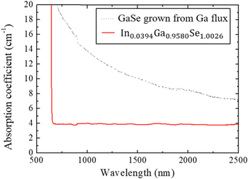
Figure 7. Absorption coefficient of the In0.0394Ga0.9580Se1.0026 mixed crystal and a GaSe crystal grown from a Ga flux in the visible to IR wavelength range.
Download figure:
Standard image High-resolution imageFigure 8 shows the absorption coefficients of In0.0394Ga0.9580Se1.0026 and a GaSe crystal grown from a Ga flux in the THz frequency range. Comparison of these reveals there is no significant difference between them. Additionally, regardless of the In composition, it is confirmed that the absorption coefficients tend to decrease as the frequency becomes higher. This is probably because phonon modes of E'(TO) and E'(LO) exist at 6.4 THz and 7.65 THz [6], respectively, and the absorption increases due to phonon vibrations near 6.4 THz and 7.65 THz.

Figure 8. Absorption coefficient of the In0.0394Ga0.9580Se1.0026 mixed crystal and a GaSe crystal grown from a Ga flux in the THz frequency range.
Download figure:
Standard image High-resolution image4.4. Results of THz wave generation
Figure 9 shows the conversion efficiency for THz waves (9.7 THz) from the In0.0394Ga0.9580Se1.0026 mixed crystal and the undoped GaSe crystal. The thicknesses of the In0.0394Ga0.9580Se1.0026 and undoped GaSe crystals were 860 μm and 100 μm, respectively. Accordingly, the maximum output energy was obtained as 73 pJ/pulse and the maximum conversion efficiency of the In0.0394Ga0.9580Se1.0026 mixed crystal was 3.1 × 10⁻⁵ J−1. In a previous paper, the conversion efficiency at 9.41 THz of an undoped GaSe crystal grown from a Ga flux was reported to be 1.2 × 10⁻⁶ J−1 [3]. The conversion efficiency obtained in this experiment is about 26 times larger than the previous value.
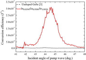
Figure 9. Conversion efficiency of THz waves at 9.7 THz and 9.41 THz as a function of the incident angle of the pump wave. (Black line: Undoped GaSe crystal, Red line: In0.0394Ga0.9580Se1.0026 mixed crystal).
Download figure:
Standard image High-resolution imageFigure 10 shows the calculated THz wave power at 9.7 THz and 9.41 THz as a function of interaction length using equation (3). When the phase matching condition is perfectly satisfied, the output power of the THz waves obtained using DFG is given by [35, 36].

where 
 and
and  are the THz peak power (W) of the pump light, the signal light and the THz waves generated via DFG, respectively,
  is the effective NLO coefficient [37],
  is the internal phase matching angle and φ is the azimuthal angle (In this study, the azimuthal angle was assumed to be 0°),
  is the angular frequency of the THz waves, n is the refractive index calculated using Sellmeier's dispersion formula [6, 38], T = 4n/(1 + n)2 is the transmittance at the crystal surface, α is the absorption coefficient,
  (
( and
and  are the absorption coefficients at 1200 nm, and
  is the absorption coefficient at the frequency of the generated THz waves), L is the interaction length of the pump and signal lights in the crystal. The interaction length L is expressed by

where t is the thickness of the InxGa1−xSe mixed crystal and  is the incident angle of the pump light at the maximum conversion efficiency (external phase matching angle), shown in figure 9. According to equation (2), the conversion efficiency (J−1) is calculated from the THz pulse energy P (J). The THz pulse energy P is equal to the value of the THz peak power I divided by the pulse width.
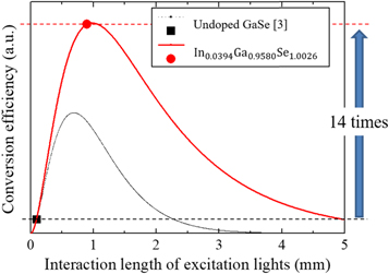
Figure 10. Conversion efficiency of THz waves at 9.7 THz and 9.41 THz as a function of the interaction length calculated by equation (3).
Download figure:
Standard image High-resolution image
The conversion efficiency calculated from the absorption coefficients (

 ) in figures 7 and 8 is shown in figure 10. In addition, the conversion efficiency at the interaction length of the excitation light calculated from the thicknesses of the In0.0394Ga0.9580Se1.0026 mixed crystal and the undoped GaSe crystal are plotted with red circles and black squares, respectively.
As shown in figure 10, it was confirmed that the conversion efficiency at the interaction length of the excitation light calculated from the thickness of the In0.0394Ga0.9580Se1.0026 mixed crystal is 14 times larger than that of the undoped GaSe crystal. The calculated ratio between the conversion efficiencies is approximately half that of our experimental value. In the calculation, the azimuthal angle was assumed to be 0°, although the azimuth angle was not actually confirmed. However, according to [31], it seems that in the azimuthal angle dependence of the output energy, the maximum output energy was nearly twice the minimum value. Therefore, it is possible that the difference between the calculated and experimental values for the conversion efficiency was caused by the difference in azimuthal angle. According to the results of the calculations, it was confirmed that the conversion efficiency of the In0.0394Ga0.9580Se1.0026 mixed crystal was at least 14 times greater than that of the undoped GaSe crystal. This is because of the increase in the interaction length of the excitation light and the improvement in transparency in the infrared range. Even without considering the improvement in transparency, the conversion efficiency is greatly improved by increasing the thickness because the conversion efficiency increases as the thickness increases. Comparing the conversion efficiencies of crystals with thicknesses of 860 μm and 100 μm on the black dotted line in figure 10 shows the conversion efficiency is increased by a factor of 7.7. The results presented here show that it is possible to increase the growth rate without loss of transmittance by growing GaSe crystals using an In flux as the solvent and increasing the interaction length for THz wave generation. From the above, it is confirmed that the increase of the growth rate and the crystal thickness contributed greatly to the progress of the generation efficiency by calculation of the conversion efficiency together with the result of the absorption characteristics in THz and NIR range.
5. Conclusion
InxGa1−xSe mixed crystals were successfully grown from an In flux by a traveling heater method. The growth rate increased compared with that of the growth of GaSe crystals from a Ga flux. According to the results of DSC, the Se solubility and the temperature coefficient of the solubility were greater in crystals grown from an In flux with GaSe at saturation compared with the case of Se dissolved in a Ga flux. By using indium as a solvent, ingot-like crystals of In0.0394Ga0.9580Se1.0026 were successfully grown by THM, and the growth rate was increased compared with the growth rate of GaSe from a Ga flux. Compared to GaSe crystals grown from a Ga flux, the transmittance of the In0.0504Ga0.9488Se1.0008 mixed crystal improved in the infrared range and there was no significant difference between the absorption coefficients in the THz range. As a result, the conversion efficiency for THz wave generation using a In0.0504Ga0.9488Se1.0008 mixed crystal was 26 times greater than that of an undoped GaSe crystal, due to the increased interaction length and the improvement in transmittance in the infrared range.
Acknowledgments
This work was partially supported by JSPS Grant-in-Aid for JSPS Fellows Grant Numbers JP18J11396, JP19J20564.
Conflict of interest
The authors declare no conflicts of interest.