


Abstract
Graphene oxide (GO) is an oxidized derivative of graphene that can be formed into free-standing wafers by aqueous processing methods. We propose GO as a potential alternative printed electronic substrate material to mitigate the waste electronic and electrical equipment problem. By dissolving these substrates in water, GO permits the mechanical separation and recovery of discrete components from defunct circuits, thus closing the life cycle of printed circuits. In this work we measure the anisotropic, frequency dependent resistivity of free-standing GO wafers under DC and AC (f = 0.1 Hz–500 kHz) excitation and in varying relative humidity (RH) conditions. Unmodified GO and GO crosslinked with calcium ions, borate ions, and glutaraldehyde were characterized. AC resistivity measurements reveal charge transport in free-standing GO occurs by several distinct hopping conduction mechanisms that are sensitive to the crosslinking formulation. GO crosslinked with calcium ions exhibits the highest DC resistivity, 4.6 × 10⁵ Ωm and 2.6 × 10⁴ Ωm, for out-of-plane and in-plane directions, respectively, at 17% RH. Both AC and DC resistivities decrease with increasing RH. We demonstrate that GO wafers can be used as dielectric substrates in the construction of simple electronic circuits with discrete electronic components. Finally, we present a proof-of-concept for electrical trace and component recovery via disassembly of GO wafers in water.
Export citation and abstract BibTeX RIS

Original content from this work may be used under the terms of the Creative Commons Attribution 4.0 license. Any further distribution of this work must maintain attribution to the author(s) and the title of the work, journal citation and DOI.
1. Introduction
Waste electrical and electronic equipment (WEEE) is a growing problem and an often overlooked contributor to the environmental crisis. WEEE is defined as any discarded electronic device or equipment incapable of performing its intended function [1]. In 2019 the world produced 53.6 Mt of WEEE, with a global annual growth of 3% year-on-year [1]. The issues associated with WEEE can be categorized as environmental toxicity, valuable resource loss, and intractable recycling processes. Closer inspection reveals that printed circuits, universally present in modern electronic devices and equipment today, are the primary contributors to these problems [2]. They are sources of toxic environmental contaminants including heavy metals and brominated flame retardants [3, 4]. Their presence in landfills also represent lost resources that are not easily recoverable, such as precious metals (e.g. gold, palladium, silver, platinum) used in semiconducting chips and other discrete components [1]. The recovery of precious metals typically includes mechanical milling of the printed circuit followed by leaching with aqua regia; a process that contributes to environmental contamination [5].
Proposed solutions to the WEEE problem aim to address end-of-life processing by presenting more efficient ways of recycling printed circuits [6], while others target the material construction of printed circuits by replacing the industry standard epoxy-resin infused composite with some variation of paper [7, 8], liquid crystal polymers [9] and bio-composite materials [10, 11]. As the most detrimental effects of printed circuits become relevant at their end-of-life, alternative constructions of printed circuits that are environmentally benign when processed at end-of-life are of high interest. We propose graphene oxide (GO) as a dielectric substrate for printed circuits. As we will later demonstrate, GO substrates offer the possibility of an aqueous based printed circuit disassembly process which enables the facile recovery of precious metals in conductive traces, discrete components, and the GO material itself.
GO is a family of layered materials derived from graphene (figure 1(a) [12]), wherein oxygen containing functional groups are bound to the underlying carbon network [13, 14]. The continuous sp2 carbon network that gives rise to delocalized π–π* electronic bands in graphene is disrupted by oxygen containing groups in GO. Generally, this results in GO having isolated conductive sp2 domains, separated by insulating sp3 regions. Electronic transport occurs by hopping conduction, as has been experimentally observed by measuring the temperature dependence of GO thin-film resistivity in both the DC [15] and AC [13, 16] regimes. These studies have also shown that GO is semiconducting or insulating depending on oxygen content. Deoxygenated GO, called reduced GO (rGO), is more similar to graphene in chemistry, structure and electronic properties, and the degree of deoxygenation can be used to tune these properties [17, 18]. GO has been used as a dielectric in monolithic field effect transistors [19], memristors [20], and humidity sensors [21]. In these works, GO serves as a dielectric with mechanical support provided by a secondary substrate. To date, GO has not been used as a free-standing substrate for electronic applications.
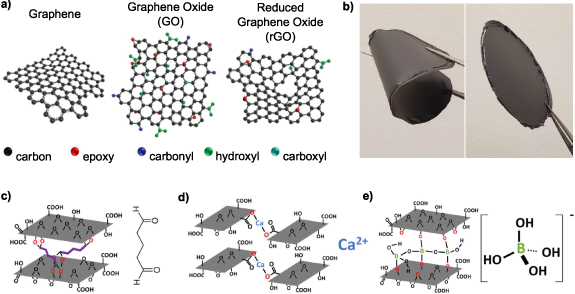
Figure 1. (a) Representative chemical structures of graphene, graphene oxide and reduced graphene oxide [12]. Reproduced from [12]. CC BY 4.0. (b) Free-standing, flexible graphene oxide wafer, 90 mm in diameter, produced by vacuum filtration. Representative structure of (c) glutaraldehyde [29], (d) calcium ion [30], and (e) borate ion [31] crosslinked graphene oxide.
Download figure:
Standard image High-resolution imageFree-standing GO structures akin to paper [22] (figure 1(b)) can be prepared using a variety of methods and was first reported by Dikin et al [23]. State-of-the-art production of these structures involves using high-density aqueous suspensions or slurries of GO, and driving GO sheet self-assembly by removing water via evaporation [24], or more commonly, vacuum filtration [25]. The addition of crosslinking agents to aqueous GO precursor suspensions has been widely studied for tuning the mechanical properties of the resulting free-standing GO structure [26–28]. Molecular crosslinking agents such as glutaraldehyde (figure 1(c)) have been shown to enhance the mechanical storage modulus of GO paper in excess of 300% [29]. The binding between GO sheets is enhanced by covalent bonding of the aldehyde groups of glutaraldehyde with the hydroxyl groups of GO. Multivalent ionic crosslinking agents such as calcium (figure 1(d)), magnesium and borate (figure 1(e)) ions, form bonds between GO sheets, enhancing the mechanical storage modulus of GO paper by a factor of two with the addition of 1 wt.% crosslinking agent [30, 31]. Bonding between an ionic crosslinker and carboxylate groups on GO sheet edges, as well as oxygen functional groups on the basal plane of GO sheets, increases the adhesion of GO sheets within the paper-like structure.
The effect of crosslinking agent and concentration on the electrical properties of free-standing GO, including the frequency dependence and anisotropy of electrical resistivity, has not been studied to date.
Finally, we note that GO is known to be hygroscopic and its conductivity is directly proportional to water content and relative humidity (RH) [32, 33]. However, GO structures are mechanically stable in humid environments [32], enabling their application in acoustic transduction, for example [34]. Moreover, prolonged immersion in hot water can cause GO to degrade into humic acid-like fragments [25]. Humic acids are a naturally occurring family of compounds found in bog peats. Yet, the toxicity of GO fragments to organisms in soil is a topic of current research [35–37]. It is thus implied that water disassembly of GO based circuits might be environmentally benign as long as residual GO fragments are recovered.
Here, we report experiments on free-standing GO to assess its suitability for use in printed circuits. The electrical resistivity of various crosslinked formulations of free-standing GO wafers was measured, including calcium ion, borate ion, and glutaraldehyde crosslinked GO as well as pure GO. Sonicated GO was also investigated with the aim of increasing resistivity by decreasing GO sheet size. The in-plane and out-of-plane electrical resistivities were measured at DC and AC (f = 0.1 Hz–500 kHz), as functions of RH. The frequency dependence of GO resistivity was found to agree with a variable range hopping conductivity model, including hopping mechanisms with distinct characteristic time scales, which we attribute to distinct physical hopping mechanisms. GO crosslinked with calcium ions exhibited the highest in-plane and out-of-plane DC resistivities. To demonstrate the GO circuit substrate concept, several simple electronic circuits with discrete components were assembled and tested using GO wafer substrates. We further demonstrated the electrical trace recovery by simple dissolution of GO substrates in warm water.
2. Methods and experiments
2.1. GO wafer fabrication
The fabrication of a GO wafer began by dispersing 2.4 g of 25 wt.% GO aqueous paste (LayerOne Advanced Materials) in 57.6 g of room temperature deionized (10 MΩ cm) water with magnetic stirring for 30 min. The dispersion was then poured into a vacuum filtration apparatus, figure 2, consisting of a porous frit and a hydrophilic polyvinylidene fluoride filtration membrane (Millipore 0.22 μm pore, 90 mm diameter, Fisher Scientific, GVWP09050), backed by a diaphragm pump at 80 kPa below atmospheric pressure. Water was extracted from the dispersion until a flat, dry GO wafer remained. The duration of the drying process was ∼36 h. The GO wafer's thickness and diameter were measured using a precision digital caliper (Mastercraft Digital Caliper GS586800). The mass retention ratio (final mass of GO wafer to total starting mass of precursory GO and dry crosslinker mass for GO wafers) was 38 ( 2)%.
2)%.
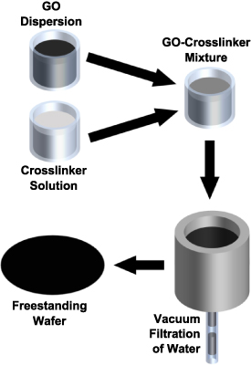
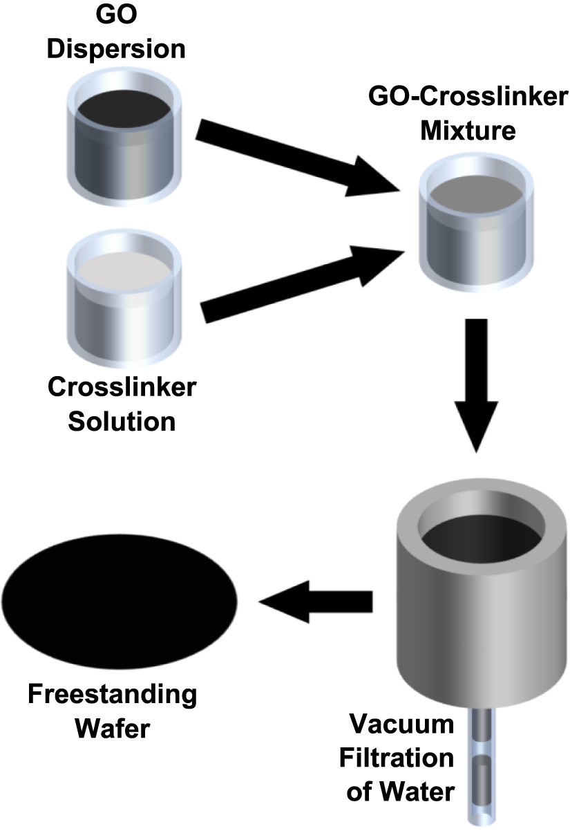
Figure 2. Vacuum-assisted filtration process for the preparation of GO wafers. The GO dispersion is mixed with crosslinking solution (omitted for plain GO wafer), and then poured into vacuum filtration apparatus. Water is removed with the assistance of vacuum applied to the filter. The dry GO wafer is then separated from the filter.
Download figure:
Standard image High-resolution imageTo produce a sonicated GO wafer, the procedure is identical, with an additional sonication step (Branson Ultrasonics MH1800) of the dispersion for 1 h after magnetic stirring.
The formulation of crosslinked GO began with 2.4 g of 25 wt. % GO dispersed in 37.6 g of deionized water. To prepare the crosslinking solution, 30 mg of crosslinking precursor was mixed with 20 ml of room temperature deionized water. In the case of anhydrous borax, 70 °C deionized water was used to aid the dissolution of borax crystals, and the resulting solution was allowed to cool to room temperature. The crosslinker precursors used in this work are calcium chloride (CaCl2,  97% Sigma Aldrich), anhydrous borax (Na2B4O7
 99%, Sigma Aldrich), and glutaraldehyde (50 wt. % aqueous glutaraldehyde solution, Fischer Scientific). Both the GO dispersion and crosslinking solution were magnetically stirred for 30 min. The crosslinking solution was then poured into the GO dispersion, with this new mixture being stirred magnetically for 1 h. While preparing calcium crosslinked GO, a change in colour to light brown and the formation of colloidal particles was observed. The crosslinker-GO mixture was then poured into a vacuum filtration apparatus, figure 2. The drying procedure was the same as that used for unmodified GO. These samples are designated Ca–GO (5 wt.%), Brx–GO (5 wt.%) and GA–GO (5 wt.%) for calcium ion, borate ion and glutaraldehyde molecule crosslinking respectively. The designator 5 wt.% refers to the ratio of crosslinker mass to the total combined mass of GO and crosslinker. The mass retention ratio (final mass of GO wafer to total starting mass) for crosslinked GO wafers was 37 (
 2)%.
2)%.
The mean wafer thickness across unmodified (17), sonicated (4), and crosslinked (6 each formulation) samples was 98 (±22) μm (see section II in supplementary material) and was measured using digital calipers with each sample being measured twice, in orthogonal directions along the basal plane.
2.2. GO sample preparation
Two classes of samples were used for resistivity measurements: an in-line distributed (ILD) contact sample and a circular parallel plate (CPP) capacitor, as shown in figures 3(a) and (b) respectively. The ILD samples were 25  3 mm wide, with 2.0
  0.5 mm wide metal electrodes separated by 6
  1 mm long gaps. The CPP sample electrodes were 11.3
  0.1 mm in diameter. The ILD and CPP samples were fabricated by first cutting the GO wafer into the appropriate geometry, followed by metal electrode formation by evaporating (3
  2 × 10⁻⁷ Torr, Nexdep, Angstrom Engineering) metals through a metal film shadow mask. The metal electrode stack used was Au/Cu/Au (20/100/80 nm). The CPP samples were fabricated by sandwiching the GO wafer between two complementary, aligned shadow masks, and evaporating metal onto each surface sequentially. Electrical connectors were attached to the metal electrodes using conductive silver paint (SPI Supplies), which was cured at room temperature for 24 h.

Figure 3. (a) ILD geometry sample to measure the in-plane complex resistivity ρ∥. (b) CPP geometry sample to measure the out-of-plane complex resistivity ρ⊥. (c) The anisotropy in resistivity arises from the directional stacking of GO sheets within a free-standing wafer. The in-plane (parallel) and out-of-plane (perpendicular) current density vectors induced by externally applied electric fields are illustrated.
Download figure:
Standard image High-resolution imageProof-of-principle demonstration circuits were assembled by securing discrete components onto a calcium ion crosslinked GO substrate via silver paint (SPI Supplies) applied to the contacts. The silver paint was allowed to dry for 1 h before a second coat was applied for additional mechanical strength. After an additional 1 h of drying, silver paint was applied to form electrical traces, and the entire assembly was dried in air at room temperature for 24 h.
2.3. Material analysis
X-ray diffraction (XRD) analysis of GO wafers was performed with a diffractometer (D8 Discover, Bruker Corp.) equipped with Cu Kα x-ray source (λ = 1.540 56 Å). A step size of 0.02° in 2θ was used. The interlayer spacing was determined from Bragg's law as d = λ/(2 sinθ). The number of samples used for these measurements are as follows: unmodified GO (4), Brx–GO (4), GA–GO (5), Ca–GO (5), and Son–GO (5).
X-ray photoelectron spectroscopy (XPS) of GO wafers was performed on a monochromatic photoelectron spectrometer (Al K-Alpha, Thermo Scientific). Three separate samples of each GO formulations were scanned for survey scans and element specific scans (C1s for all samples, Ca2p for Ca–GO and B1s for Brx–GO). Survey scans were collected between 0 and 1200 eV with a step size of 1 eV for each sample. Elemental high-resolution scans were performed with a step size of 0.1 eV. Spectrum deconvolution was done with software (Thermo Avantage, version 5.9). Binding energies were calibrated by setting the C1s binding energy to 284.8 eV. Carbon spectra were deconvolved into four components, C–C (284.8 eV), C=O (288.2 eV), C–O (286.8 eV), and π−π* shake up (290.7 eV).
The cross-sectional structure of GO wafers was imaged with a scanning electron microscope (SEM) at 15 kV acceleration voltage and secondary electron imaging (FlexSEM1000, Hitachi). The GO wafers were manually fractured, and sputter coated with platinum (thickness ∼4 nm).
The GO sheet distribution was measured by optical reflection microscopy. Unmodified and sonicated GO suspensions were drop-cast onto a Si wafer with 300 nm of SiO2 for optical contrast enhancement. The suspensions were dried and imaged under white light.
2.4. Electrical measurements
DC and AC resistivity measurements were conducted by sealing electrical samples in a container with two Kinyanco hygrometer thermometers to monitor RH and temperature. The RH inside the sealed vessel was regulated using saturated salt solutions [38, 39]. 17%, 32%, 51%, 73%, and 86% RH were achieved using saturated lithium chloride, magnesium chloride, magnesium nitrate hexahydrate, sodium nitrate, potassium nitrate, respectively. A second set of samples were measured at ambient RH (∼25%) for comparing the frequency dependence of complex resistivity between samples.
DC resistivity measurements were performed using a Keithley 4200A-SCS semiconductor parameter analyser with a linear sweep of current from 0 to a maximum between 1 nA to 100 nA (ILD samples) and 0.1 μA to 10 μA (CPP samples) depending on sample resistance. AC impedance measurements were conducted using a Zurich Instruments MFLI 500 kHz/5 MHz lock-in amplifier. The AC voltage rms amplitude was set at 707 mV (ILD samples) and 7.07 V (CPP samples) while frequency was swept logarithmically. As shown in figure 3, the anisotropic structure of GO originating from GO sheet stacking leads to two distinct directions in which resistivity can be measured: in-plane resistivity,  , along the basal plane of the structure and out-of-plane resistivity,
  , perpendicular to the basal plane of the structure. The in-plane resistivity determines the resistance of the ILD geometry samples, as shown in figure 3(b), and the out-of-plane resistivity determines the resistance of the CPP geometry samples, as shown in figure 3(c), with negligible corrections expected from current spreading effects.
DC resistivity of ILD samples was measured using both a two-point configuration and a four-point configuration, with the latter arranged with current applied to and collected from the outer contacts and voltage measured across the inner contacts. There was less than ∼7% deviation between two-point and four-point measurements for all samples (see supplementary material section V). DC measurements of CPP samples were conducted in a two-point configuration.
All AC resistivity measurements were conducted in a two-point configuration for both CPP and ILD samples. The complex resistivity was extracted from geometric factors and the complex current and voltage,

where A is the GO cross-sectional area and L is the GO length oriented for in-plane or out-of-plane conduction geometries.
2.5. Circuit disassembly
50 ml of deionized water in a Pyrex dish was heated to 69 °C. A metallized GO sample was submerged in the water and the circuit disassembly process was recorded on video over approximately 10 min.
3. Results and discussion
3.1. Material analysis
The layered anisotropic structure of the GO wafers was imaged in cross-section by SEM, presented for all formulations in figure 4(a). It is thus expected that GO wafers exhibit anisotropic physical properties, including electrical resistivity.
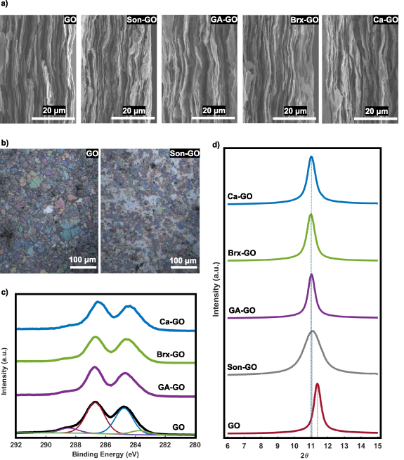
Figure 4. (a) Cross-sectional SEM images of unmodified GO, Son–GO, GA–GO, Brx–GO, and Ca–GO wafers. (b) Optical microscope images of unmodified and sonicated GO suspensions dispersed on Si/SiO2 for optical contrast enhancement. (c) XPS C1s spectra of unmodified GO, Ca–GO, Brx–GO, and GA–GO wafers normalized to count of unmodified GO spectrum. Deconvolution of GO C1s spectrum: C–O (red—286.7 eV), C–C (blue—284.8 eV), C=C (green—283.6 eV), C=O (purple—288.3 eV) and π−π* (cyan 290.4 eV). (d) XRD spectra of unmodified GO, Son-GO, Ca-GO, GA-GO, and Brx-GO with their specified interlayer distance.
Download figure:
Standard image High-resolution imageThe unmodified GO flakes used to prepare all formulations, and the sonicated GO flakes were dispersed in dilute concentration (0.001 g ml−1), and imaged optically on Si/SiO2 substrates, as shown in figure 4(b). The optical microscope images clearly demonstrate a significant decrease in GO flake size after sonication. In addition to providing a representation of the dispersion in GO sheet shape and size, thickness variation can also be observed. The 300 nm thickness of the SiO2 on Si provides an interferometric enhancement in reflection contrast which leads to a colour shift versus sheet thickness sufficient to observe monolayers [40]. The negligible presence of monolayer GO in the images of figure 4(b) indicates that GO sheets form multi-layer aggregates, as has been previously observed [41].
XPS revealed no significant difference in composition between samples despite varying formulations. C/O atomic ratios varied slightly between samples (figure 5(a)): 2.19 (±0.01) for unmodified GO, 2.13 (±0.05) for GA–GO, 2.11 (±0.07) for Brx–GO, and 2.21 (±0.11) for Ca–GO. However, only the decreases in C/O for Brx–GO and GA–GO are statistically significant. This result is explained by the fact that borate ions and glutaraldehyde are oxygen containing molecules, and therefore introduce more oxygen into the material, thus decreasing the C/O ratio. Numeric elemental composition is reported in the supplemental material section III. Deconvolution of the C1s spectrum into C=C (283.6 eV), C–C (284.8 eV), C–O (286.7 eV), C=O (288.3 eV) and π−π* (290.4 eV) yielded the typically recorded waveforms and peak positions [42] for GO, despite differing formulations (figure 4(c)). For the C1s spectrum C=C contributes 1.81 (±1.39)%, C–C contributes 41.6 (±2.6)%, C–O contributes 52.4 (±1.7)%, C=O contributes 3.82 (±0.44)%, and π−π* contributes 0.320 (±0.070)%. In the case of borate and calcium ions, this similarity in the C1s spectra can be attributed to the concentration of ionic crosslinkers being below XPS detection limit, yielding no noticeable spectral differences (see XPS surveys for Ca2p and B1s spectra in supplementary material section III). Glutaraldehyde, being an organic compound containing only carbon, hydrogen, and oxygen, is difficult to resolve in GO by XPS. With a high enough resolution C1s scan and sufficient mass percentage of glutaraldehyde, we would expect to see an increase in the spectral contributions of C–C and to a lesser degree C–O bonds compared to unmodified GO. Statistical analysis of deconvolution of the C1s spectrum for GA–GO relative to unmodified GO showed that measured variations for all types of carbon bonds were statistically insignificant (see supplementary material section IV).
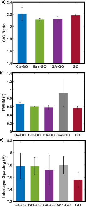
Figure 5. XRD average (a) full width at half maximum and (b) interlayer spacing with error bars representing one standard deviation from the mean. (c) XPS average C/O ratio histogram with error bars representing one standard deviation from the mean.
Download figure:
Standard image High-resolution imageXRD was performed on all formulations of GO wafers. The diffraction intensity versus 2θ is shown in figure 4(d), and the average interlayer spacing, and full width at half maximum (FWHM) is shown in figures 5(b) and (c) respectively. The unmodified GO has an interlayer spacing of d = 7.55 (±0.12) Å, well within the range of values typically reported for GO [43]. Modified GO shows larger interlayer spacing ranging from 7.78 (±0.14) Å observed in Brx–GO to 7.80 (±0.14) Å observed in Son–GO, as the increase for GA–GO is statistically insignificant (see supplementary material section IV). This increase in interlayer spacing by similar amounts for different crosslinking agents is in agreement with previously reported trends [43–46]. Water content has been reported to increase interlayer spacing [47], however, hydration can be eliminated as the reason for increased interlayer spacing by thermogravimetric analysis (material figure S7), which indicates negligible variation in water content across samples. Also, previously reported XRD data shows that dehydrating GO, even for 5 min, decreases the interlayer spacing by as much as 2.6 Å [47]. Our wafers are dehydrated using vacuum pumping for ∼36 h.
The inter-layer spacing depends weakly upon the specific crosslinking agent use as can be seen in figure 5(b). The ionic crosslinkers (borate and Ca2+) appear to yield larger interlayer spacing. Sonicated GO also shows an increase in the FWHM; from 0.56° (±0.03°) for unmodified GO to between 0.66° (±0.05°) for GA–GO and 0.92° (±0.32°) for Son–GO. However, the FWHM increases for GA–GO and Brx–GO are statistically insignificant (see supplementary material section IV). The increase in the FWHM indicates a decrease in stacking density of ordered domains in sonicated GO, which has been attributed to two effects. There is an increased density of oxygen functional groups on smaller GO sheets produced by sonication [48], and there is a less compact and more disordered stacking behaviour of smaller GO sheets [49].
3.2. Resistivity measurements
The in-plane and out-of-plane AC resistivity of Ca–GO (figures 6(a) and (b)), Brx–GO (figures 6(c) and (d)) and GA–GO (figures 6(e) and (f)) are presented in the form of Nyquist plots of −Im(ρ) versus Re(ρ) over the frequency range f = 0.1 Hz–500 kHz. Additionally, the Nyquist resistivity plots for GO sonicated for 1 h (figures 6(f) and (g)) and unmodified GO (figures 6(i) and (j)) are given for comparative purposes. The Nyquist plots reveal the anisotropy of GO wafer resistivity ( ), in both magnitude and functional dependence upon frequency.
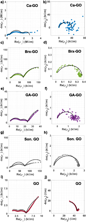
Figure 6. In-plane and out-of-place complex resistivity Nyquist plots for (a)–(b) Ca–GO, (c)–(d) Brx–GO, (e)–(f) GA–GO, (g)–(h) Son. GO (1 h) and (i)–(j) unmodified GO over the frequency range 0.1–500 kHz. Experimental measurements (solid marks) and hopping conduction model fit (black solid line) are shown.
Download figure:
Standard image High-resolution imageVariable range hopping is the primary electronic conduction mechanism in GO and lightly reduced GO [14]. A characteristic of variable range hopping in disordered materials is the presence of a broad distribution of hopping lengths between the localized states participating in the conduction process, thus leading to a broad distribution in hopping rates [50].
A simple and broadly applicable analytical model for the frequency dependent resistivity associated with hopping conduction is given by [51]
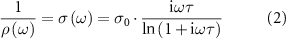
where  is the DC conductivity, and
  is the lower limit of the frequency distribution of electron hopping. This model hopping conduction model corresponds to a single arc in a Nyquist plot, where the scale of the resistivity arc is determined by
  , and
, and  sets the frequency scale that defines the low-frequency (
 ) and high-frequency (
 ) limits. In the low-frequency limit,
  , while in the high-frequency limit,
  , corresponding to a capacitive shunt impedance as expected from a Miller–Abrahams circuit model of hopping conduction [52].
To account for the multiple arcs observed in the Nyquist plots of the measured resistivities in figure 6, we propose a simple model consisting of a series combination of resistivities each describing distinct frequency dependent hopping conduction,
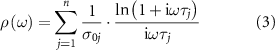
where  , and
, and  are the DC conductivity and lower limit of the electron hopping frequency distribution for hopping process j. This composite model was fit to the experimentally measured GO resistivities of figure 6 (solid black lines), with the resulting model parameters
  , and
, and  listed in table 1. The number of distinct hopping conduction processes leading to good agreement between model and experiment varies depending upon the GO formulation and the resistivity component,
  or
or  .
.
Table 1. In-plane and out-of-plane variable range hopping model parameters determined by fitting to the measured complex resistivity of GO wafers with various formulations.
| Sample | ρ | σ01 (S m−1) | σ02 (S m−1) | σ03 (S m−1) | τ1 −1 (s−1) | τ2 −1 (s−1) | τ3 −1 (s−1) |
|---|---|---|---|---|---|---|---|
| Ca–GO | ∥ | 2.5 × 10⁻⁶ | 1.7 × 10² | ||||
| ⊥ | 3.8 × 10⁻⁶ | 7.0 × 10⁻⁷ | 1.0 × 10⁻⁶ | 2.0 × 10⁵ | 1.0 × 10³ | 1.0 × 101 | |
| Brx–GO | ∥ | 2.7 × 10⁻³ | 1.0 × 10⁵ | ||||
| ⊥ | 1.5 × 10⁻⁴ | 1.6 × 10⁻⁵ | 7.0 × 10⁻⁶ | 5.0 × 10⁵ | 3.3 × 10³ | 3.3 × 10⁻¹ | |
| GA–GO | ∥ | 6.5 × 10⁻⁴ | 2.4 × 10⁴ | ||||
| ⊥ | 7.5 × 10⁻⁵ | 1.0 × 10⁻⁴ | 2.0 × 10⁻⁵ | 1.7 × 10⁵ | 3.3 × 10³ | 1.3 × 10⁻¹ | |
| Son. –GO | ∥ | 4.0 × 10⁻⁴ | 1.7 × 10⁴ | ||||
| ⊥ | 1.3 × 10⁻⁴ | 1.5 × 10⁻⁵ | 1.0 × 10⁻⁵ | 1.0 × 10⁵ | 6.7 × 10² | 6.7 × 10⁻¹ | |
| GO | ∥ | 2.2 × 10⁻² | 7.7 × 10⁻² | 2.0 × 10⁶ | 1.2 × 10⁻¹ | ||
| ⊥ | 3.8 × 10⁻⁴ | 3.7 × 10⁻⁴ | 6.0 × 10⁻⁵ | 1.1 × 10⁶ | 3.3 × 10⁴ | 1 × 10⁻¹ |
We thus propose that electronic conduction in an assembly of GO sheets in a GO wafer involves distinct hopping processes as illustrated in figure 7. These processes include: (i) electron hopping between sp2 domains within a GO sheet, (ii) electron hopping between sp2 domains of adjacent GO sheets within an aggregate of GO sheets, and (iii) electron hopping between sp2 domains of GO sheets in adjacent aggregates of GO sheets. It is further possible that there are distinct mechanisms contributing to processes (i)–(iii), as there is a variety of physical phenomena including polaron formation and electron–electron interaction that can play a role in hopping conduction [50]. While it is not possible to definitively attribute the experimentally observed hopping conduction model parameters  , and
, and  with the hopping processes (i)–(iii), the general trend is that the highest DC conductivity and fastest hopping rate is expected for (i) electron hopping within a GO sheet, and progressively smaller conductivity and slower hopping rate for (ii) and (iii), electron hopping between GO sheets and GO sheet aggregates. In view of the hopping conduction model described above, the Nyquist plots of figure 6 reveal several important trends. The in-plane resistivity
  is well described with a single hopping conduction process, which is most likely process (i), electron hopping within GO sheets. Process (i) accounts for the largest fraction of hopping steps for charge moving in-plane and is anticipated to be the dominant impedance contribution at high frequency. The sole exception is unmodified GO (figure 6(j)), where a second slower (smaller
  ) conduction mechanism is evident at low frequency (f ≪ 30 kHz), which is likely of type (ii) or (iii). The slower type (ii) or (iii) hopping process contribute impedances
 at lower frequencies, but present a negligible, capacitive impedance
  at high frequency (f ≫ 30 kHz). In crosslinked and sonicated GO, increased intra-sheet spacing as observed directly by XRD and/or smaller GO sheets are anticipated to further slow (decrease
  ) type (ii) and (iii) hopping processes, and therefore require lower frequencies f to probe the resistivity associated with these processes. The out-of-plane resistivity
  reveals the contribution of distinct mechanisms over the same measurement frequency range. This is expected, as out-of-plane charge transport entails a different distribution of hopping steps of types (i)–(iii) as compared to in-plane transport. The magnitude of the resistivities |
 | and |
 | versus frequency f at ambient RH (24%) are shown in figures 8(a) and (b). The least resistive GO in both transport directions is unmodified GO, as anticipated on account of the tight GO sheet aggregation and minimal processing of the GO sheets. Ca–GO is the most resistive. Sonicated GO shows an increase in resistivity compared to unmodified GO, expected from GO sheet damage and fracture incurred by sonication. Crosslinking further increases in-plane and out-of-plane resistivity, with Ca–GO (5 wt.%) being the most resistive GO found in this study for frequencies f < 30 kHz in the out-of-plane direction. We also observe that GO treatments do not affect
  and
and  equally. For example, sonicated GO is more resistive in-plane than Brx–GO (5 wt.%), while Brx–GO (5 wt.%) is more resistive out-of-plane than sonicated GO. While the increased inter-plane spacing induced by crosslinking is expected to increase resistivity as compared to unmodified GO, the variation in resistivity among crosslinked GO cannot be explained by the near-constant inter-plane distance observed via XRD. Further work is required to elaborate the relation between the nature of the crosslinking agent and GO treatment, and the effect upon hopping transport processes.
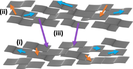
Figure 7. Electron variable range hopping processes within GO; intra-monolayer hopping (i-blue), inter-monolayer hopping (ii-orange), inter-aggregate hopping (iii-purple).
Download figure:
Standard image High-resolution image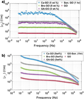
Figure 8. Absolute magnitude of the measured (a) in-plane and (b) out-of-plane resistivity versus frequency for various formulations of GO.
Download figure:
Standard image High-resolution imageThe asymptotic high-frequency behaviour of in-plane resistivity  (figure 8(a)) is observed in all samples. Neglecting the slowly varying logarithmic dependence on frequency, the conduction model predicts a high-frequency resistivity
  , in line with the capacitive reactance of the Miller–Abrahams circuit model of hopping conduction in the high-frequency limit [50]. The effective permittivity defining the capacitance in this circuit model is
  , whose values are determined from the model parameters of table 1 and summarized in table 2. A physical interpretation of
  is the effective capacitive coupling between the conductive sp2 domains participating in hopping conduction. In the case of in-plane conduction, the effective capacitive coupling is approximately invariant between samples, which suggests that crosslinking does not affect the capacitive coupling between sp2 domains. Moreover, this asymptotic high-frequency behaviour is not observed for out-of-plane resistivity (figure 8(b)). Further experimental work is required to determine how GO processing affects the effect.
Table 2. Effective capacitance associated with the model fit hopping conduction parameters of table 1 for in-plane and out-of-plane hopping conduction, and various GO formulations.
| Sample | ρ |
 1 (F m−1) 1 (F m−1) |
2 (F m−1) |
3 (F m−1) |
|---|---|---|---|---|
| Ca–GO | ∥ | 1.5 × 10⁻⁸ | ||
| ⊥ | 1.9 × 10⁻¹¹ | 7.0 × 10⁻¹⁰ | 1.0 × 10⁻⁷ | |
| Brx–GO | ∥ | 2.7 × 10⁻⁸ | ||
| ⊥ | 3.0 × 10⁻¹⁰ | 4.8 × 10⁻⁹ | 2.1 × 10⁻⁵ | |
| GA–GO | ∥ | 2.7 × 10⁻⁸ | ||
| ⊥ | 4.4 × 10⁻¹⁰ | 3.0 × 10⁻⁸ | 1.5 × 10⁻⁴ | |
| Son. –GO | ∥ | 2.4 × 10⁻⁸ | ||
| ⊥ | 1.3 × 10⁻⁹ | 2.23 × 10⁻⁸ | 1.5 × 10⁻⁷ | |
| GO | ∥ | 1.1 × 10⁻⁸ | 6.4 × 10⁻¹ | |
| ⊥ | 3.5 × 10⁻¹⁰ | 1.1 × 10⁻⁸ | 6.0 × 10⁻⁴ |
The in-plane and out-of-plane DC resistivity of different GO samples are shown in figures 9(b) and (d). For all formulations of GO, the DC  is at least one order of magnitude larger than the DC
  , as anticipated from the anisotropic structure of GO. Ca–GO exhibits the highest DC resistivity in-plane and out-of-plane among the various formulations of GO. These resistivities are uniform across the area of the 90 mm GO wafers (see supplementary material table S8). There is a 4–9 order of magnitude of difference between the resistivities of Ca–GO, other proposed materials in literature and the industry standard FR4. FR4 is a fibreglass epoxy composite ubiquitously used as a printed circuit dielectric substrate with a volume resistivity on the order of ∼1010−1016 Ωm [53, 54]. Another proposed material system to combat the environmental effects of printed circuits is phthalated acrylated epoxidized soybean oil mixed with styrene, divinylbenzene, and halogen-free flame retardant, laminated with hybrid fibres (PASD-FR/H) and phthalated acrylated epoxidized soybean oil mixed with styrene, and divinylbenzene, laminated with hybrid fibres (PASD/H). These are composite laminates of chicken feathers and glass fibres epoxidized with soybean oil-based resins, with PASD-FR/H containing a halogen-free melamine polyphosphate and diethylphosphinic salt as a flame retardant [10]. Both materials have volume resistivities on the order of ∼1013 Ωm [10].
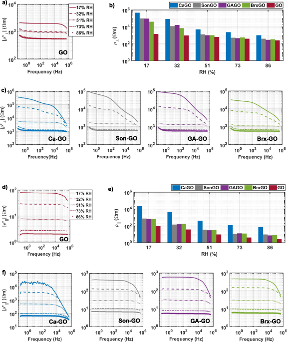
Figure 9. Relative humidity dependent DC (b and h) and complex in-plane (a and c) and out-of-plane (d and f) resistivities for various formulations of GO.
Download figure:
Standard image High-resolution imageBoth the complex and DC resistivities in all formulations of GO decrease with an increase in RH, in agreement with previous reports on GO thin films [22, 32]. This phenomenon has been explained as a consequence of GO's hygroscopic nature, with the increase in water content facilitating ionic conduction via dissolved ionic impurities [31]. We find that the order of magnitude of both | | and |
 | at 86%RH is approximately the same, and independent of frequency over the measurement range, regardless of the initial resistivity at 17% RH, with exceptions for unmodified GO |
 | and |
 |, and Ca–GO |
 |. This trend cannot be definitively explained using the presented data and requires further experimental work.
Since Ca–GO exhibited the highest resistivity observed overall, attempts were made to fabricate Ca–GO with higher calcium ion concentration. Increasing the ratio of calcium chloride precursor to GO results in inhomogeneous crosslinker incorporation and mechanical failure (see supplementary material section I).
3.3. Demonstration circuits
As a proof-of-principle, simple circuits were constructed with Ca–GO to demonstrate GO wafer functionality as a printed circuit substrate. The sheet resistance of the (100 ± 10 μm) thick Ca–GO substrate used is 476 MΩ
 −1. The first demonstration circuit constructed is a simple light emitting diode circuit, featuring a 58 Ω resistance in series with a light emitting diode operated at 3.3 V supplied by an external battery. The circuit, shown in figures 10(a) and (b), was assembled with silver paint acting as the conductive traces and adhesive for discrete components.
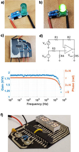
Figure 10. (a) LED demonstration circuit with power off. (b) LED demonstration circuit with power on. (c) Inverting operational amplifier demonstration circuit. (d) Operation amplifier circuit schematic. (e) Gain and phase curve of amplifier circuit. (f) Clock circuit in operation.
Download figure:
Standard image High-resolution imageThe second circuit demonstrated is an analogue inverting amplifier, shown in figures 10(c) and (d), operated with a 5 V supply. Details of the circuit parameters are provided in table S9 of the supplementary material. The measured gain,  , and phase
  versus frequency f for an input excitation of Vin = 0.707 V are shown in figure 10(e).
The third circuit demonstrated is a digital clock circuit that uses a microcontroller to keep track of time, while displaying the current time using a four-digit seven segment display. Pushbuttons allow for the adjustment of the hours and minute digits. The design of the circuit parameters are provided in supplementary material figure S8 and table S10.
The functionality of AC and DC circuits has thus been demonstrated. Consequently, while the resistivity of GO is significantly less than that of FR-4, the Ca-GO wafer resistivity is nonetheless sufficiently high for niche but wide range of circuits.
3.4. Circuit disassembly
It is desirable to achieve facile recovery of metals, discrete components, and the circuit substrate material at the end-of-life of a printed circuit assembly, without the need for milling and leaching [5]. To demonstrate metal recovery with a GO substrate, a disassembly test was performed.
A metallized (Au/Cu/Au) unmodified GO circuit was immersed in a 69 °C de-ionized water bath. Digital pictures taken during the first 10 min of immersion are presented in figure 11. After 5 s, the conductive traces began delaminating from the GO substrate. Delamination was complete after approximately 30 s. After delamination, the metal could be collected by physical separation in the water bath. After approximately 10 min, the GO substrate lost mechanical integrity, fracturing upon any further manipulation. The GO fragments swell in size, notably in thickness, as the re-suspension of GO in water proceeds.

Figure 11. Proof of principle for recycling process for non-functioning graphene oxide. (a) Metallized circuit on unmodified GO substrate. (b) Circuit submerged in water at 69 °C. (c) Delamination and separation of metal film from GO substrate. (d) GO loss of mechanical integrity and disintegration.
Download figure:
Standard image High-resolution image
These results suggest a pathway to a closed lifecycle for printed circuits with GO as the dielectric substrate. Circuits at end of life could be immersed in water, and discrete elements and metal traces could then be physically separated or filtered, leaving behind GO in the process of re-suspension. The removed circuit elements and metals could be reprocessed and reused, without the need for milling and leaching as in conventional printed circuit technology.
4. Conclusion
We have characterized the resistivity of GO wafers with various crosslinking preparations, permitting the identification of distinct hopping conduction mechanisms using a modified hopping conduction model. We have further shown that calcium ion crosslinked GO (5 wt.%) has the highest resistivity at low frequency (f < 30 kHz) among the formulations compared. We demonstrated the possibility of assembling circuits with discrete components, and have shown how metal traces and components can be recovered by dissolution of the GO substrate in water.
Further work is required to understand the microscopic origins of the various hopping conduction mechanisms in GO, and to subsequently devise strategies to increase GO resistivity over a larger bandwidth, and minimize the reduction of resistivity with increasing humidity, while maintaining the ability to disassemble the material with water. This work entails the study of a wider range of crosslinking and functionalization strategies that exploit the unique chemistry of GO functional groups. Furthermore, mechanical characterization of the material, contrasted against mechanical properties of current printed circuit substrates is required. The investigation of other graphene derivatives, such as hydrogenated graphene [55], offers further opportunities to explore the limits to achievable resistivity, insensitivity to humidity, and facile aqueous disassembly.
Finally, we note the future opportunity to realize a completely metal free printed circuit technology based on GO and rGO. Laser induced thermal reduction of GO with additives such as carbon nanodots enhance rGO conductivity as compared to pure rGO [56, 57], suggesting the possibility of selective area deoxygenation of GO to produce conductive rGO traces atop insulating GO for a completely metal-free circuit substrate technology.
Acknowledgments
The authors acknowledge financial support from the Natural Sciences and Engineering Research Council of Canada (NETGP 508526-17, STPGP 506395-17), and the technical assistance of Pascal Bourseguin and Dr Kaiwen Hu.
Data availability statement
The data cannot be made publicly available upon publication because no suitable repository exists for hosting data in this field of study. The data that support the findings of this study are available upon reasonable request from the authors.
Supplementary data (9.3 MB MP4) Video of a functioning clock circuit on a GO wafer substrate.
Supplementary data (9.6 MB MP4) Video of water disassembly of a GO circuit.
Supplementary data (1.0 MB PDF) Additional characterization of free-standing GO wafers and GO wafer circuits.