


Abstract
In this study, software and hardware that supported automatic optical inspection (AOI) for printed circuit board production line was proposed and demonstrated. The proposed method showed an effective solution that predicts off-line electromagnetic (EM) characteristic of manufactured components through in-line pattern integrity. A spiral antenna that represented complex patterns was used as the evaluation target with imitated production variations. Numerical evaluation on EM properties, batch fabrication, hardware setup and optimization, algorithm and graphical user interface development, machine learning and artificial intelligence modeling, and data verification and analysis were thoroughly conducted in this study. Results indicated that when the antenna showed pattern distortion, its passive capacitance, active intensity, and active frequency increased, decreased, and decreased, respectively. These results proved that the developed system and method overcame the inability of in-line EM measurement in conventional setup. The results also showed high estimation accuracy that was not yet achieved in the past. Compared to existing or similar AOI ideas, the proposed method supports analyses on complex pattern, provides solutions on target design, and efficient algorithm generation. This work also proved active and passive EM signals with evidences, and exhibited outstanding confidence levels for characteristic estimations. The proposed system and method indicated their potential in smart manufacturing.
Export citation and abstract BibTeX RIS
1. Introduction
Automatic optical inspection (AOI) is a crucial and an inevitable quality assurance in manufacturing industry [1–3]. AOIs appeared repeatedly in production lines, in which multiple fabrication steps existed, to assure that expected profile or quality were generated for specific products before they were passed to the next fabrication step. Because AOI could quantify specific features of designated analysis target (for example, the dimension of a partial area in the complete space through image contrast comparison), users are able to set different targets and their specifications at different AOI steps. When the AOI result is out of the preliminarily set range, standard operation procedures (SOPs, such as re-work or scrap) can be conducted. AOI has became a mature technique and thus been widely used in various non-microelectronic industrial applications (e.g., packaging, drilling, and welding) [4–6]. In these applications, in practice, although production variations left negative impacts on the aesthetic appearance or information clarity, out-of-spec. products could still be used. For example, a misaligned chromaticity printing on the wrapping paper does not alter its function.
Nevertheless, in microelectronic production lines, potential issues appear because active or negative electrical activities were realized through multilayer interconnects [7]. Fabrication variations (such as pattern distortion or shift) in a single layer could lead to disconnected signals between layers. Unfortunately, electrical characteristic or electromagnetic (EM) performance of microelectronic components cannot be evaluated in-line (real-time along fabrication). Their performance can only be understood when the fabrication reached a specific step or even the complete component is finalized. In an extreme case, although the performance of a component is already suspected incorrect in some process steps in a production line, it cannot be confirmed in advance. Manufacturers could only continue the fabrication steps before the component is completed, wasting valuable materials, time, and manpower.
As a result, microelectronic industries have built multiple AOI steps in their production lines and set individual inspection target (for example, holes generated through etching in photolithography on semiconductor materials). In addition, corresponding fabrication variations and their controllabilities (for example, ±5%) were set to those targets (for example, a lower and an upper limit of the hole dimension). However, even though these activities helped on maintaining the designed features of the component, they are not necessarily required. For instance, an out-of-spec. hole distorted from circular to elliptical shape could still transmit electrical signals between two layers in a printed circuit board (PCB). Consequently, this AOI step and its related SOPs become time-consuming drawbacks from the cost viewpoint. In contrast, for another instance, a straight line could distort with wavy edges. Even though it could pass the AOI (because usually average linewidth is inspected in a segment) [8], it fails to indicate potential issues such as broken line or current crowding-induced reliability concern of local heating. Consequently, AOI unfortunately did not yet efficiently point out the risk in the production line. The aforementioned examples were all consequences of the fact that a practical solution, which is able to predict the off-line EM characteristics of microelectronic components from their in-line fabrication features, is missing.
Although literature has indicated potential relationships between pattern distortion and its EM performance [9–13], they failed to provide solutions to predict the results. Researchers also tried to establish related system and procedures to predict some responses of Archimedean spiral antennas through their fabrication features, results were incomplete due to impractical target design, non-optimized software and hardware modules, insufficient data, low confidence level of results, and non-integrated human–machine interface (table 1) [14, 15].
Table 1. Highlights between the present and existing works. C, I, and f represents capacitance (in unit of pF), intensity (in unit of dB), and frequency (in unit of GHz) values of the evaluation samples, respectively. R2 and RMSE represents coefficient of determination and root-mean-square error of collected data, respectively.
| [14] | [15] | This work | |||||
|---|---|---|---|---|---|---|---|
| Target | Single arm | Two arms | Two arms | ||||
| Unequal BA | Unequal BA | Equal BA | |||||
| Label for ML | Passive (capacitance) | Passive (capacitance) | Passive (capacitance) | ||||
| Active (frequency) | Active (intensity and frequency) | ||||||
| Analysis | Manual | Manual | Automatic | ||||
| Data quantity | Training | Testing | Training | Testing | Training | Testing | |
| 60 | 18 | 144 | 36 | 960 | 240 | ||
| R2 | C | 0.64 | NA | NA | NA | 0.976 | 0.969 |
| I | NA | NA | NA | NA | 0.785 | 0.775 | |
| f | NA | NA | 0.98 | NA | 0.988 | 0.982 | |
| RMSE | C | 0.408 | 0.309 | NA | NA | 0.0843 | 0.0849 |
| I | NA | NA | NA | NA | 3.5212 | 3.4599 | |
| f | NA | NA | 0.0044 | 0.0109 | 0.0048 | 0.0051 | |
To overcome the disadvantages of existing systems, this work adopted identical analysis procedure from our previous work [15], however improved the target antenna distortions with equal bulge amplitudes (BAs) on both edges of both arms with additional signal for analysis, and revised machine learning (ML) and artificial intelligence (AI) models. As a result, the novelty and contribution of this paper are summarized as follows: (1) integrated hardware and software through a human–machine interface and (2) improved AOI and AI for accurate predicted EM characteristics.
2. Method
2.1. Fundamental pattern
Based on the referential literature [15], the fundamental Archimedean spiral was described by (1) in the Cartesian coordinate, in which a, b, and t were constant, constant, and sector angle, respectively. To meet the EM operation requirements (frequency of 2–6 GHz that supports Wi-Fi and Bluetooth applications), a, b, and t were defined as 0.591, 1, and 4.28π–12.86π, respectively; and the resulting pattern was 15 cm-long with line width (w) and line space (s) both 0.93 mm. When two identical Archimedean spirals were interlaced however with a 180° rotational difference, a self-complementary Archimedean spiral antenna (SCASA) was achieved (figure 1(a)). Although the idea was proposed for PCB industry as an example, imitating reasonable pattern distortions resulted by rheology that appeared in other printed microelectronics (such as by inkjet printing) was also the aim of the present work. Thus, SCASA was the evaluation patterns and this work introduced its distorted counterparts through mathematical methods for comparison
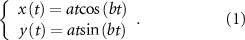
Figure 1. Illustrative SCASAs in literature with BA of (a) 0.00 (reference), (b) 0.15, and (c) 0.30 in the previous work [15]. Clearly, pattern deviations can be found in (b) and (c), and (c) is worse than (b). Reproduced from [15]. © IOP Publishing Ltd. All rights reserved.
Download figure:
Standard image High-resolution imageIn printed microelectronics, inks or solid contents accumulate owing to surface tensions and other rheological properties [16]. Regular ink accumulations could be found not only because of the pattern design [17] but also the printing sequence of the system [18]. As a result, repeated bulges and neckings appear on the patterns and literature described this effect by duplicating them through sinusoidal equations [15] with (2). The constant 25 in (2) indicated that there were 25 bulges along one arm. It was clear that a point P varies its location on the Cartesian coordinate due to the changing parameters of not only the fundamental spiral but also additional factors of BA and displacement (d, in unit of mm) from the smooth edge. Large BA was resulted by large d from its original location defined only by (1). Straightforwardly d = 0 led to a BA = 0.00 or 0% distortion; d = 0.93 led to a BA = 1.00 or 100% distortion. In short BA = 0.00 was the reference and the two arms touch with each other when BA = 1.00. Even though bulges and neckings were repeatedly generated through (2), the pattern was impractical because bulges enlarge as the spiral develops with the sector angle (figures 1(b) and (c)). Consequently, additional correction on generating constant bulges in a SCASA was needed.
2.2. Revised SCASA
In the aforementioned regard, this work introduced some correction factors, which helped on suppressing the enlarging bulge along the enlarging sector angle. As described in (3), the constant 25 in the sine operation in (2) was revised as a variable ωt, in which ω represent the angular frequency. As a result, along the increment of t, BA was suppressed. With appropriate ω, which was set to 0.3 in this work, similar bulge dimensions could be found regardless of the sector angle, reflecting practical cases in solid content accumulation during inkjet printing. In this work, BAs of 0.00 (figure 2(a)), 0.15, 0.30 (figure 2(b)), 0.45, 0.60 (figure 2(c)), and 0.75 were evaluated
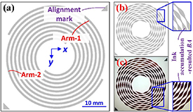
Figure 2. The target SCASA in the present work with BA of 0.00 (reference) design, (b) 0.60 design, and (c) 0.60 on fabricated PCB. Clearly, bulges in this work repeatedly appeared in a SCASA, which reflects practical ink accumulation behaviors.
Download figure:
Standard image High-resolution image2.3. Fabrication
From (3), not only the fundamental (reference)SCASA but also SCASA with five BAs were generated as evaluation targets. The six SCASA patterns were fabricated by single-sided PCB process, and 200 samples were fabricated through identical process for each SCASA design. To appropriately control the process tolerance, the SCASAs were manufactured by a foundry service (Ping-Yi Electronics Co., Ltd), who assured a less than ±100 μm variation. The PCB fabrication was started from mask design, substrate (35 μm thick copper on 0.4 mm thick FR4) exposure, development, etching, before deionized water cleaning and nitrogen blow was conducted for the finished sample (figure 2(c)). Due to the limited fabrication tolerance, process variation did not lead to ambiguous analysis result, which will be explained later. In addition, because BA is positively related to line edge roughness (LER), this work also analyzed the LERs of SCASAs by an existing AOI method [14].
Because both arms of the SCASA were conductors and the material between the two arms was dielectric, the SCASA already exhibited passive capacitive response after fabrication. Consequently, six capacitances appeared in simulated results (figure 3(a)) as the theoretical values. In addition, this work also focused on active EM responses of SCASAs in terms of intensity and frequency. Thus, the six SCASA patterns were also simulated for their corresponding results (figures 4(a) and (b) for intensity and frequency, respectively). Besides simulated passive and active results, each sample was also measured for the labels, which will be used during AI establishment. Among the fabricated 1200 samples, 80% (960 pieces) and 20% (240 pieces) were defined as the training and testing group, respectively.
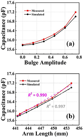
Figure 3. Relationships between the measured or simulated capacitances and (a) BA and (b) arm length. These results indicate that capacitance is a function of arm length, which in turn is a function of BA. Dashed lines in (b) indicate the linear fits.
Download figure:
Standard image High-resolution image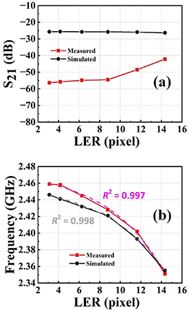
Figure 4. Relationships between the LER and the measured and simulated (a) intensity and (b) frequency. These results imply that the intensity and frequency is independent and dependent on the LER or BA. Dashed lines in (b) indicate the reversed exponential fits.
Download figure:
Standard image High-resolution image2.4. Analysis
From the LER on each sector angle on each edge of each arm, features for ML (such as line width, line space, and pattern area) can be collected. In addition to the features, labels (active intensity and frequency, and passive capacitance of the SCASA) defined for ML were also collected. The SCASA intensity and frequency were obtained through vector network analyzer (Agilent, E5071C) with Yagi–Uda transmitter/receiver [19], which will be explained later; and the SCASA capacitance was detected through the capacitance digital converter (Analogue Devices, AD7746) with the official evaluation kit.
ML was performed with a training group of samples through the lazy learning method in commercial software MATLAB (version 2021b) with toolbox of Regression Learner App, which returned various potential AI models. Besides the training group, the rest samples were defined as the testing group and their features were fed into those AI models to generate the predicted results (labels) with different R2s and RMSEs. In this work, the samples in both the training and testing groups had their corresponding measured features and labels, but only the samples in the testing group had their corresponding predicted labels through AI models. Consequently, the correctness of the AI model could be determined by comparing the difference between the measured and predicted labels of the samples in the testing group; and this work chose the results with the largest R2 and the smallest RMSE as the AI model.
Additionally, this work also simulated the active and passive responses of the SCASAs with six BAs, which was defined as the simulated values. Because one SCASA design only had a single set of simulated values, the eligibility of the proposed method could be proved by comparing the simulated and predicted label sets.
Although the three SCASA labels (i.e. intensity, frequency, and capacitance) still need to be collected through separate systems; the aforementioned LER analyses, feature collection, ML, AI modeling, and characteristic prediction were all automatically performed through an integrated graphical user interface (GUI). By using the GUI, not only the operation simplicity was enhanced, efficiency and accuracy were simultaneously improved when compared with other works that introduced manual operations.
3. Result and discussion
3.1. Relationship between BA and LER
After analyzing the LERs of the fabricated SCASA patterns, results indicated an expected tendency: LER increased as BA enlarged (figure 5). This not only proved that the pattern distortion could be scientifically quantified and qualified but also the proposed workflow and algorithm were correct. Even though large variation existed in the reference (BA = 0.00) and BA = 0.15 groups, the rest four groups exhibited limited tolerance, indicating that the PCB fabrication was reliable. Furthermore, the differences between BA groups were noticeable: the largest LER in the former BA group never surpassed the least LER in the latter BA group. Consequently, these LERs were eligible to be included in the ML as the feature. Although the LER did not necessarily show a linear relationship to the BA, linear fit showed a R2 = 0.966 when averaged LER in one BA group was used.

Figure 5. Relationships between the LER and BA from all 1200 samples. This result exhibits a positive relationship between the LER and BA as expected.
Download figure:
Standard image High-resolution image3.2. Passive (capacitive) response
On passive responses, the capacitance values increased as the BA (or LER) increased (figure 3(a)), which followed the expectation. This result was straightforward because when the LER worsened, the arm length increased. In the SCASA, the arm length and Cu thickness (an independent but constant parameter in this work) formed the area of the capacitor drawn in figure 2(a). As a result, the prolonged arm length due to the worsened LER increased the area of the capacitor, which led to the enlarged capacitance value. Furthermore, the arm length was 441.45, 442.03, 443.57, 446.12, 449.66, and 454.16 mm for 0.00, 0.15, 0.30, 0.45, 0.60, and 0.75 BA designs, respectively; and a nonlinear relationship existed between LER and BA was found as shown in figure 5. However, as mentioned earlier, the arm length had a positive relationship with the area of the capacitor, which in turn had a positive relationship with the capacitance value. Consequently, high confidence levels (simulated and measured results showed R2 of 0.997 and 0.990, respectively) were obtained from linear fits (figure 3(b)), indicating the correctness of the analyzed passive responses.
3.3. Active (intensity and frequency) response
On active responses, the simulated results followed the expectation because the coupling efficiency increased as the capacitance values increased [15], which led to the decay of transmitted intensity S21 (figure 6(a)) in the detection setup (figure 7). However, the measured results showed a reversed tendency (figure 6(b)). This could be attributed to three potential reasons. First possibility was the environmental tolerance, which failed to isolate surrounding noises around the detection setup. Secondly, the Yagi–Uda antenna emitted EM waves in a broadening manner instead of keeping them as plane waves throughout the detection system. Thirdly, as BA (or LER) worsened, imperfect Cu in the neckings appeared easier, leading to reduced coupling efficiency.

Figure 6. (a) Simulated and (b) measured active response of the intensity along frequency. These EM responses indicate that the experimental results follow the simulation predictions even though reasonable tolerance existed during detection.
Download figure:
Standard image High-resolution image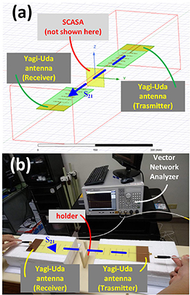
Figure 7. The Yagi–Uda antennas and active response detection setup in (a) simulation model (scale bar of 300 mm) and (b) practical experiment. The EM signal starts from the transmitter, passes through the SCASA, and enters the receiver before being analyzed. Note that the slot for the SCASA in (b) was empty and the cables were not connected yet.
Download figure:
Standard image High-resolution imageIn case of frequency, the operating point (in which the weakest intensity located) moved to lower frequency as the BA (or LER) worsened, which matched the tendency of simulated results with a negative relationship in an exponential manner (R2 were 0.998 and 0.997 for simulated and measured frequency, respectively), as shown in figure 6(a). These environmental or operational tolerance could be avoided in the future when better setups are available.
3.4. ML and AI modeling
To this point, the required feature (LER) and labels (capacitance, intensity, and frequency) were all collected from the samples of the training group for ML. Even though there were various ML methods and it was not the only solution to use ML to establish the AI model, this work introduced lazy learning when considering the complexity of the aforementioned relationships among all features and labels.
Lazy learning results indicated that the model developed with Gaussian progress regression with covariance function of exponential exhibited the largest R2 and the smallest RMSE. Based on these quantified evidences, this result was considered the AI model of this work, which was an independent module from the AOI and GUI for simplicity of the system and practicality of hardware or software revisions when need.
To validate the accuracy of the established AI model, not only individual pattern variations in samples of the testing group was analyzed but also their active and passive responses were examined. When the LERs of individual samples were fed into the AI model, the proposed system output the predicted corresponding capacitances, intensities, and frequencies of the SCACAs. Results indicated that, on the passive response, the predicted and measured capacitance showed a positive relationship to the BA (figure 8). Although some results overlapped with each other in the BA groups of 0.00 and 0.15, the difference between the predicted and measured data was less than 0.481% in a single BA group (of 0.45). Taking the measured capacitance of the samples in the testing group as the reference, the difference between the predicted and measured results was merely 0.404% on average through (4). In addition, the result of linear fit exhibited a high confidence level with R2 of 0.969, indicating that the established AI model was practical (table 1)
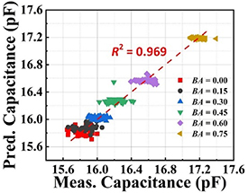
Figure 8. The distribution of predicted and measured capacitances and their relationship. M. (Meas.) and P. (Pred.) in the legend or axial title represent measured and predicted, respectively. A good linearity and high confidence level of linear fit can be observed between the M and P capacitances.
Download figure:
Standard image High-resolution imageSimilarly, on the active responses, the predicted and measured intensity results also showed good linearities regardless of intensity (figure 9) or frequency (figure 10). As mentioned earlier, because the active responses were influenced by the passive responses, some data overlapped with each other when negligible distortions (BA of 0.00 and 0.15 groups) existed regardless of intensity or frequency. However, the accuracy of the AI model was compatible to that used for passive responses. The difference between the predicted and measured results for intensity and frequency was less than 7.11% (worst case appeared in the BA 0.30 group) and 0.192% (worst case appeared in the BA 0.45 group), respectively. Taking the measured intensity of the samples in the testing group as the reference, the difference between the predicted and measured results was only 4.925% on average with R2 of 0.775. Similarly, taking the measured frequency of the samples in the testing group as the reference, the difference between the predicted and measured results was only 0.166% on average with R2 of 0.982.
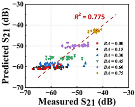
Figure 9. The distribution of predicted and measured intensities and their relationship. M. and P. in the legend represent measured and predicted, respectively. Even though the confidence level between the M and P intensities is not as good as that between the M and P capacitances (figure 8), a linear tendency is still noticeable.
Download figure:
Standard image High-resolution image
Figure 10. The distribution of predicted frequencies and their relationship with corresponding measured values. M. (Meas.) and P. (Pred.) in the legend or axial title represent measured and predicted, respectively. A good linearity and high confidence level of linear fit can be observed between the M and P frequencies.
Download figure:
Standard image High-resolution imageTo this point, the proposed AI-assisted characteristic prediction system for PCB production lines through AOI was demonstrated. The established AI model not only successfully predicted the three labels (capacitance, intensity, and frequency) of the SCASAs from the feature (LER) with different distortions in the testing group but also showed outstanding accuracy to the measured data, when compared with existing studies.
4. Conclusion
In summary, compared with other similar works, this work proposed and provided newly developed software and hardware, showcasing an integrated AOI system that was supported by ML and AI. From the software viewpoint, various functions were integrated through the GUI with automatic operations. From the hardware viewpoint, modularized image capturing and capacitance measurement setups provided stability and accuracy. This system was able to predict the off-line passive and active responses of microelectronic components from their in-line fabrication integrity. With SCASA demonstrations made by standard PCB process and intentionally generated pattern distortions, the AI model exhibited high accuracies on all three labels (R2 of 0.969, 0.775, and 0.982 for capacitance, intensity, and frequency, respectively; RMSE of 0.0849 pF, 3.4599 dB, and 0.0051 GHz, for capacitance, intensity, and frequency, respectively). In addition, the tolerance that was defined in (4) was 0.404%, 4.925%, and 0.166% for capacitance, intensity, and frequency, respectively. These results showed compatible performance to practical PCB production lines and exhibited three novelties when compared with existing works: (1) the evaluation patterns were practical for inkjet-printing, (2) the LERs and related analyses were automatically conducted without manual operations, and (3) higher accuracy and efficiency analyses with the GUI (figure 11).

Figure 11. The developed GUI in this work, which includes sequential operation steps of image capturing (upper left), contrast enhancement (upper right), contour extraction (lower left), LER analysis with characteristic prediction (lower right), and status indicators to the right.
Download figure:
Standard image High-resolution image
Although SCASAs were introduces as demonstrations in this work, the proposed system and workflow also supports other applications. The system showed good compatibility when being applied onto other simple linear (such as line width and line space in circuits) or nonlinear (such as holes for interconnects) patterns. When the image capturing device (i.e. camera) supports high resolution in different wavelengths, not only the analyzed accuracy could be improved but also multilayer PCB inspection could be conducted. By using the proposed system, material and manpower costs could be noticeably suppressed regardless of re-work or scrap. The automatic operation was also helpful on avoiding erroneous operations, which was generally and frequently found in operators who do not have professional or technical backgrounds in production lines.
Acknowledgments
This study was partially supported by the Ministry of Science and Technology, Taiwan (MOST108-2628-E-007-002-MY3).
Data availability statement
The data cannot be made publicly available upon publication because they are not available in a format that is sufficiently accessible or reusable by other researchers. The data that support the findings of this study are available upon reasonable request from the authors.