

Abstract
There is an increasing demand for low-cost and high-performance electronics which has stimulated a need for new high-performance dielectric materials. We have developed a facile synthesis of poly(2-(methacryloyloxy)ethyl trimethylammonium bis(trifluoromethylsulfonyl)azanide-ran-methyl methacrylate) (P(METATFSI-MMA)), a polymeric ionic liquid that can be used as a high-performance dielectric for semiconducting single walled carbon nanotube (SWCNTs) thin film transistors (TFTs). The P(METATFSI-MMA) polymer was synthesized at both 35 and 62 mol% of 2-(methacryloyloxy)ethyl trimethylammonium bis(trifluoromethylsulfonyl)azanide and produced p- and n-type devices that functioned under ambient conditions. These TFTs were then used to study the impact of electrochemical doping on the performance of SWCNT TFTs when switching from n-type, where an electrical double layer is formed, to p-type, where the TFSI− anions are free to interact with the SWCNTs. The TFTs operating in p-type had higher current on/off ratios and a larger transconductance than those operating in n-type, which is characteristic of electrochemically doped transistors. Furthermore, we tested the impact of operating frequency on device performance and discovered that decreasing the operating frequency of the TFTs resulted in a decreased hysteresis. The decrease in hysteresis was also observed to be more significant for the 35 mol% polymer.
Export citation and abstract BibTeX RIS

Original content from this work may be used under the terms of the Creative Commons Attribution 4.0 license. Any further distribution of this work must maintain attribution to the author(s) and the title of the work, journal citation and DOI.
1. Introduction
Thin film transistors (TFTs) [1, 2] can be printed onto flexible/stretchable substrates and operated at low voltages, making them attractive for use as high performance (μA currents, 104 and higher on/off current ratios) TFTs in wearable electronics and sensing applications [3–9]. Low-voltage (<3 V) devices are especially in demand to help reduce the power consumption of fabricated TFTs as well as the size of battery used to power the device. However, achieving low-voltage operation requires either a very thin dielectric or a dielectric material with a high capacitance density [10, 11]. Traditional polymer dielectrics such as poly(methyl methacrylate) (PMMA), poly(styrene) (PS) and poly(vinyl phenol) are limited in their applications. This is due to their low capacitance densities [12] and the challenge of high-throughput processing of pin-hole free and uniform <100 nm films [3, 13]. Alternatively, the use of electrolytes provides a thickness-independent dielectric due to the formation of an electrical double layer (EDL) as a result of the mobile ions. Traditionally, organic electrochemical transistors (OECTs) are fabricated using ionic liquids [14, 15] or aqueous salt electrolytes as the dielectric, which facilitates the formation of an EDL [16]. This corresponds to an accumulation of ions at the semiconductor/dielectric interface, which leads to a greater local electric field and ultimately a greater capacitance [17, 18]. The high capacitance density increases charge carrier density at the semiconductor interface, resulting in larger on-currents and reduced operating voltages [19]. However, electrolyte gated devices suffer from poor stability and low switching speeds. Additionally, the devices have a liquid gate, which is not ideal for solid state applications [16, 20, 21]. Some of these issues are mitigated by gelling the electrolyte using a polymer additive to create a solid device that exhibits EDL formation [22]. Regardless, during operation, the mobile ions in the dielectric diffuse into the semiconductor. This is referred to as electrochemical doping and can cause slow device switching speeds. Alternatively, poly(ionic liquids) (PILs) can be synthesized to achieve the same thickness-independent EDL operation as electrolytes while avoiding electrochemical doping. PILs have one ion bound to the polymer structure with a free moving counter-ion. This allows for quasi-ionic liquid performance with the benefit of having a solid film at room temperature. When a voltage is applied the free ions (cations for p-type transistor operation, or anions for n-type) diffuse to the gate electrode interface while the corresponding polymer-bound counter-ions move to the PIL/semiconductor interface; the counter-ions are too big to diffuse into the semiconductor [23, 24]. However, PILs tend to have lower ionic conductivities than electrolytes due to the increased difficulty for the ions to diffuse through the rigid polymer media [25]. Researchers have demonstrated improved conductivity by reducing the glass transition temperature (Tg) of the PIL [23, 26]. If the Tg drops too much and the films suffer from poor mechanical stability, they will become tacky and their processing becomes challenging [26]. The use of block copolymers combining a low Tg PIL block and a high Tg block enables high ionic conductivity without sacrificing the macroscopic mechanical properties of the dielectric [27]. While the block copolymer approach is a promising route, it does increase the complexity of the synthesis and the self-assembly. To further improve device performance, semiconducting single walled carbon nanotubes (SWCNTs) are used as the semiconductor. SWCNTs are among the most promising semiconducting materials for high performance and low voltage organic electronic devices [28–30]. This is due to their outstanding electrical and mechanical properties [31–33]. SWCNTs have been known to achieve carrier mobilities >100 cm2 V−1 s−1 with high output currents and large on/off ratios [34]. These devices can also operate as both p- and n-type transistors. Despite this, the vast majority of studies report p-type electrical behaviour due to their poor air stability and electron suppression in ambient environments [35–37].
In this study, we demonstrate the easily synthesized poly(2-(methacryloyloxy)ethyl trimethylammonium bis(trifluoromethylsulfonyl)azanide-ran-methyl methacrylate) (P(METATFSI-MMA)) as a dielectric in top-gate bottom-contact SWCNTs TFTs (figure 1). By varying the weight percentages of 2-(methacryloyloxy)ethyl trimethylammonium bis(trifluoromethylsulfonyl)azanide we could tune the frequency-dependent EDL formation and corresponding capacitance density. We characterized this novel dielectric by operating the TFTs at different frequencies in both p- and n-type operation. Although SWCNTs are ambipolar, under ambient conditions oxygen doping suppresses n-type behaviour due to the O2/H2O redox couple [36]. To mitigate the issue of oxygen doping we fabricated the devices in a top gate architecture so that the P(METATFSI-MMA) dielectric could encapsulate the semiconducting layer and preserve n-type performance under ambient conditions [38]. Where as many studies have looked into using SWCNTs with ionic gels/liquids [39–41], this is the first study to use PILs to fabricate p- and n-type SWCNT TFTs that operate under ambient conditions. Under p-type operation the TFSI− anions are free to diffuse and interact with the SWCNTs monolayer giving them properties like that of OECTs. Under n-type operation the device operates as high performing TFTs. The change in electrical properties of the SWCNT, including transconductance, hysteresis and on/off ratios were highly dependent on the PIL structure and operating frequency.

Figure 1. (a) Chemical structure of P(METATFSI-MMA) random copolymer poly(ionic liquid) (PIL) with 35 mol% and 62 mol% TFSI- functionalized 2-(methacryloyloxy) ethyl trimethylammonium moieties(DMAEMA); (b) 3D rendering of top gate bottom contact SWCNT based TFTs, and (c) graphical representation of both p-type and n-type operation of the PIL and SWNT TFT.
Download figure:
Standard image High-resolution image2. Experimental
2.1. Materials
The 4,4'-azobis(4-cyanopentanoic acid) (ACPA) (98%), (4-cyanopentanoic acid)-4-dithiobenzoate (97%), 2-dimethylaminoethyl methacrylate (98%), iodomethane (99%), and methyl methacrylate (MMA) (99%) were purchased from Sigma-Aldrich (MO, USA) and used as received. ACPA were recrystallized from methanol before use. The 2-(dimethylamino)ethyl methacrylate (DMAEMA) was distilled over potassium hydroxide under reduced pressure; MMA was distilled under reduced pressure. Lithium bistrifluoromethanesulfonimidate (LiTFSI, 98%) was purchased from Oakwood Chemical and used as received. Diethyl ether, dichloromethane (DCM), dimethyl formamide (DMF), and hexane were purchased from Caledon Chemical (Caledon, ON) and used as received. Chromium-coated tungsten rods (Cr) and gold (Au, 99.99%) were purchased from Angstrom Engineering. Quartz coated glass substrates (15 mm × 20 mm) were purchased from Ossila Limited. The 1 in2 glass substrates were purchased from University Wafers.
2.2. Polymer synthesis
2.2.1. Poly(methyl methacrylate) (PMMA)
MMA (4.7 g, 46.9 mol), ACPA (11.1 mg, 0.04 mmol), (4-cyanopentanoic acid)-4-dithiobenzoate (28.1 mg, 0.1 mmol), and DMF (2 ml) were placed in a flask equipped with a stir bar and purged with nitrogen for 1 h. The polymerization was conducted at 90 °C for 18 h. The reaction mixture was diluted with DCM and the polymer was isolated by precipitation in methanol. The polymer was dissolved in DCM and reprecipitated in methanol. After drying in vacuo, 2.31 g of polymer was obtained. (Mn = 27 700 g mol−1, Đ = 1.19, 25% yield) 1hydrogen-Nuclear magnetic resonance (H-NMR) (400 MHz, CDCl3,Tetramethylsilane (TMS), δ ppm): 0.84, 1.02, and 1.21 (–CH3), 1.57 and 1.81 (–CH2-), and 3.60 (O–CH3). The 1H-NMR spectrum and the size exclusion chromatogram are presented as supporting information, figures S1 and S2.
2.2.2. Poly(dimethylaminoethyl methacrylate-ran-methyl methacrylate) P(DMAEMA-MMA)-62%
DMAEMA (3.3 g, 20.8 mmol), MMA (2.8 g, 28.2 mol), ACPA (11.1 mg, 0.04 mmol), (4-cyanopentanoic acid)-4-dithiobenzoate (29.1 mg, 0.1 mmol), and DMF (3 ml) were placed in a flask, equipped with a stir bar, sealed with a septum, and purged with nitrogen for 1 h. The polymerization was conducted at 90 °C for 18 h. The reaction mixture was diluted with DCM and the polymer was isolated by precipitation in a mixture of diethyl ether/hexane (1:2). The polymer was dissolved in DCM and reprecipitated in diethyl ether/hexane (1:2). After drying in vacuo, 1.48 g of polymer was obtained. (Mn = 39 500 g mol−1, Đ = 1.18, 24% yield) 1H-NMR (400 MHz, CDCl3, TMS, δ ppm): 0.86, 1.02, 1.22, and 1.39 (–CH3), 1.80 and 1.86 (–CH2-), 2.26 (N–CH3), 2.58 (N–CH2-), 3.60 (O–CH3), and 4.04 (O–CH2-). The peaks at 3.60 ppm (O–CH3 from MMA) and 4.04 ppm (O–CH2- from DMAEMA) were used to determine the polymer composition (62% DMAEMA, 38% MMA). The 1H-NMR spectrum and the size exclusion chromatogram are presented as supporting information, figures S1 and S3.
2.2.3. P(DMAEMA-MMA)-35%
DMAEMA (2.2 g, 14.2 mmol), MMA (2.8 g, 28.2 mol), ACPA (11.1 mg, 0.04 mmol), (4-cyanopentanoic acid)-4-dithiobenzoate (28.0 mg, 0.1 mmol), and DMF (2 ml) were used in the polymerization as described above, 2.88 g of polymer was obtained. (Mn = 38 500 g mol−1, Đ = 1.33, 58% yield) 1H-NMR (400 MHz, CDCl3, TMS, δ ppm): 0.82, 0.99, 1.19, and 1.40 (–CH3), 1.78 and 1.87 (–CH2-), 2.25 (N–CH3), 2.53 (N–CH2-), 3.56 (O–CH3), and 4.03 (O–CH2-). The peaks at 3.56 ppm (O–CH3 from MMA) and 4.03 ppm (O–CH2- from DMAEMA) were used to determine the polymer composition (35% DMAEMA, 62% MMA). The 1H-NMR spectrum and the size exclusion chromatogram are presented as supporting information, figures S1 and S4.
2.2.4. Poly(2-(methacryloyloxy)ethyl trimethylammonium iodide-ran-methyl methacrylate) P(METAI-MMA)-35% and 62%
P(DMAEMA-MMA)-62% (0.64 g, 2.3 mmol DMAEMA repeat units) was dissolved in DMF (20 ml) and iodomethane (6.84 g, 48.2 mmol) was added to the solution. The reaction mixture was heated at 40 °C overnight. The excess iodomethane was evaporated and the remaining solution was dialyzed against water. The water was evaporated, in a 250 ml flask, and the polymer was obtained as a coating inside the flask after drying in vacuo. The 1H-NMR (400 MHz, D2O, δ ppm): 1.01 (–CH3), 2.00 (–CH2-), 3.31 (N–CH3), 3.71 (O–CH3), 3.86 (N–CH2-), and 4.53 (O–CH2-). Complete conversion was confirmed using the integrals of the signals at 3.31 (N–CH3) and 4.53 (O–CH2-). In addition, the signal from N–CH3 shifted downfield (supporting information, figure S5).
Quaternization of P(DMAEMA-MMA)-35% (0.63 g, 1.4 mmol repeat units) was conducted in a similar manner as above using iodomethane (6.84 g, 48.2 mmol). The 1H-NMR (400 MHz, D2O, δ ppm): 1.05 (–CH3), 2.04 (–CH2-), 3.32 (N–CH3), 3.69 (O–CH3), 3.88 (N–CH2-), and 4.54 (O–CH2-) (supporting information, figure S6).
2.2.5. Ion exchange
The polymers were each separately dissolved in DMF (20 ml), in the flask used in the quaternization step, and to the solutions was added lithium bis(trifluoromethanesulfonyl)imide (LiTFSI, 2.6 g (9.06 mmol) for P(METAI-MMA)-62% and 1.6 g (5.57 mmol) for quaternized P(METAI-MMA)-35%). The resulting solutions were stirred overnight. The polymers were precipitated in water, filtered, and washed with water. About 0.9 g of P(METATFSI-MMA)-35% and 1.1 g of P(METATFSI-MMA)-62% were obtained after drying in vacuo at 80 °C. The presence of the TFSI− anion was confirmed by [19] fluorine-nuclear magnetic resonance (F-NMR) (supporting information, figure S7).
1H NMR spectra were obtained with a Bruker Avance II 400 MHz spectrometer.
Size exclusion chromatography (SEC) was performed on a Malvern Omnisec, equipped with Omnisec Resolve pump and autosampler (CHR7100) with two T6000M columns and Omnisec Reveal (CHR6000) differential refractive index, diode-array-based UV/Vis spectrometer, and Viscotek SEC-MALS 20 multi-angle light scattering detectors. DMF with 0.01 M LiBr was used as the eluent at 40 °C with at a flow rate of 0.5 ml min−1. The dn/dc values (0.059 for PMMA, 0.061 for P(DMAEMA-MMA)-62% and 0.062 for P(DMAEMA-MMA)-35% ml g−1) for the polymers were determined by the instrument using a PMMA standard as a reference in the same eluent.
2.3. Dielectric and semiconductor preparation
P(METATFSI-MMA) solutions were prepared under ambient conditions. P(METATFSI-MMA) was dissolved in 2-butanone at a concentration of 80 mg ml−1 and filtered using 0.45 μm filters.
The semiconducting SWCNTs were prepared using a poly(9,9ʹ-didodecylfluorene-co-N-(2ʹ-decyltetradecane)-carbazole) polymer in toluene following previously reported procedures [42]. The PCF synthesis has also been reported for dispersions of SWCNTs prepared via plasma growth and purchased from Raymor Nanointegris (diameter ∼ 1.5 nm, length 0.3–4 μm) [43]. The SWCNT dispersions were not filtered prior to use [44]. The concentration of SWCNTs in the dispersion was estimated from the S22 peak height using UV–vis–near infrared (NIR) spectroscopy (figure S8). The dispersion concentration was adjusted so that the peak height was 1.5 a.u.
2.4. Thin film characterization
A Bruker dektak XT profilometer was used to determine the thickness of the fabricated PIL films.
2.5. Metal–insulator–metal capacitor fabrication
Metal–insulator–metal capacitors were fabricated on 1 in2 glass substrates. The substrates were cleaned using a four-step cleaning process where the substrates are sonicated for 5 min in soapy water, distilled water, acetone, and methanol sequentially and dried under a stream of nitrogen. Following the cleaning process 5 nm of chromium (Cr) and 50 nm of gold (Au) were deposited sequentially onto the glass substrates using physical vapour deposition (PVD) and a shadow mask. Next, 200 μl of the PIL solution at 80 mg ml−1 was spin-cast dynamically onto the 1 in2 glass substrates at 2000 rpm for 90 s under ambient conditions using a Laurell WS-650-23 spin coater. The substrates were then annealed under vacuum for 1 h at 130 °C. Finally, 50 nm of Au was deposited through a shadow mask using PVD. This yielded ten metal-insulator-metal (MIM) capacitors per substrate with surface areas from 0.35 to 2.88 mm2. About 20 MIM capacitors were fabricated for each polymer.
2.6. Metal–insulator–metal capacitor characterization
A Methrohm PGSTAT204 was used to perform potentiostatic impedance measurements with an amplitude of 10 mV within the frequency range of 10−2–105 Hz. Both the dielectric constant  and the capacitance Ci
can be calculated using the equations below where Z' is the real portion of the impedance, Z'' is the imaginary portion of the impedance, t is the film thickness, ω is the angular frequency (
and the capacitance Ci
can be calculated using the equations below where Z' is the real portion of the impedance, Z'' is the imaginary portion of the impedance, t is the film thickness, ω is the angular frequency ( , A is the area of the capacitor and
  0 is the permittivity of a vacuum:
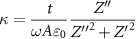

The capacitance equation can then be divided by the area of the capacitors to give the capacitance density.
2.7. TFT fabrication
TFTs were fabricated on 15 × 20 mm quartz coated glass substrates. The same cleaning procedure used for the metal–insulator–metal capacitors was used to clean the Ossila substrates. Next, the source-drain (SD) electrodes (5 nm Cr, 50 nm Au) with a width of 1000 µm and a length of 30 µm were deposited onto the substrate through a shadow mask using PVD. A 5 nm chromium layer was used to facilitate gold adhesion to the substrate. Next, the substrates were submerged in a 1% solution of octo-trichloro silanes (OTSs) in toluene overnight at 70 °C to create a thin OTS layer on the substrate. The OTS layer increases the hydrophobicity of the substrate and improve SWCNT deposition [42]. Following the OTS treatment, the SWCNTs were deposited through a drop casting technique. SWCNTs dispersed in toluene were sonicated for 15 min. Next, 0.5 μl of the sc-SWCNT dispersion was deposited between the SD electrodes via drop casting. This was repeated for each individual transistor. The entire substrate was rinsed four times with 1000 μl of toluene to remove any excess unbound polymer leaving a mono layer of SWCNTs. The rinsed substrates were then dried using a steady stream of nitrogen and annealed in air at 200 °C for 1 h. After depositing the SWCNTs, the PIL layer was deposited by spin coating. About 200 μl of PIL solution at 80 mg ml−1 was spun onto the substrate dynamically at 2000 RPM for 90 s and then annealed under vacuum at 130 °C for 1 h. Finally, the gate electrode was deposited onto the PIL layer using PVD (50 nm, Au). This allows for the fabrication of 20 individual transistors per substrate. About 20–40 transistors were fabricated for each polymer.
2.8. TFT characterization
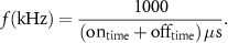
A Keithley 2614B with custom LabVIEW software was used to characterize the electrical properties of the TFTs. The TFTs were characterized using a custom-built probe station designed by Element Instrumentation Inc. and Kreus Design Inc. (oesProbe A10000-P290). The measurements were performed under ambient conditions and the transfer curves were measured in the linear region. The output curves were all measured at 10 Hz. The transfer curves were taken at various frequencies by taking measurements while pulsing the gate on and off. By changing the on/off time with the following equation, the TFTs can be tested at a set frequency:
The following equation was used to model the source-drain current (ISD) in the linear regime:
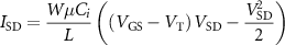
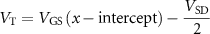
where L and W are the channel length and width, μ is the mobility, Ci is the capacitance density, VT is the threshold voltage, and VSD and VGS are the source-drain and gate-source voltages. The following equations were used to calculate VT and gm [45] in the linear regime:

The hysteresis was calculated as the absolute difference in threshold voltage between the forward and reverse sweeps of the transfer curves. The on/off current ratios (ION/OFF) were calculated using the minimum and maximum currents.
3. Results and discussion
Well-defined poly(dimethylaminoethyl methacrylate-ran-methyl methacrylate) random copolymers (P(DMAEMA-ran-MMA)), with 35 or 62 mol% of METATFSI, were synthesized by reversible addition–fragmentation chain-transfer polymerization. The polymers underwent a simple quaternization reaction followed by ion exchange to provide the bis(trifluoromethylsulfonyl)azanide (TFSI−) counter ion, to produce P(METATFSI-MMA). Full polymer characterization can be found in the supporting information. Metal insulator metal capacitors were fabricated on glass substrates and characterized using a potentiostat over a 10−2–105 Hz frequency range. Figure 2 shows the development of an EDL as a function of copolymer composition for the PILs with 0% (pure PMMA baseline), 35 mol% and 62 mol% of ionic METATFSI repeat units. In figure 2(b) the initial change in -phase angle from approximately 90° till 45° is considered the dipolar relaxation regime where the polymer itself begins to align with the applied electric field. Next, anything under 45° and until the curve return above 45° is considered the ionic relaxation regime where mobile ions begin to diffuse towards the negative or positively charged electrodes. Once the -phase angle curve has returned above 45° it is considered in the EDL formation regime and when the curve plateaus the EDL is considered fully formed [18]. For the 62 mol% sample the EDL is almost fully formed at 1 Hz whereas for the 35 mol% sample, the EDL has not fully formed at frequencies as low as 10−2 Hz. The frequency at which the EDL forms is dependent on several factors such as the glass transition temperature (Tg), as well as the size of the free ion [46, 47]. The lower Tg allows for softer films facilitating the movement of the free ions through the PIL and larger ions increase the conductivity. For this study, both polymers were functionalized with TFSI− ions. However, increasing the percentage of METATFSI from 35 mol% to 62 mol% resulted in a decrease in the Tg from 99 °C to 88 °C (figure S9). The lower glass transition temperature facilitates the migration of TFSI− anions through the polymer layer, which likely leads to an increase in the frequency at which the EDL begins to form [27, 48]. This suggests that increasing the mol % of METATFSI leads to an increase in device performance by lowering Tg. However, if the Tg is too low the films become tacky, which is not desirable.
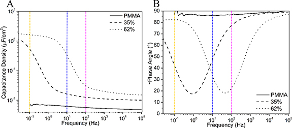
Figure 2. Frequency dependent capacitance density and -phase angle measurements of the capacitors fabricated using PMMA and P(METATFSI-MMA) random copolymer PILs with 35 mol% and 62 mol% ionic repeat units, between 10−2 and 105 Hz. Dotted lines represent the frequencies used to characterize the TFTs in figures 4 and 5.
Download figure:
Standard image High-resolution imageThe ion conductivity for both the 35 and 62 mol% samples was calculated using the parallel resistance from a circular fit to the semi-circle portion of the Nyquist plots obtained through EIS (figure S10). The conductivity (σ) is calculated from the thickness (d), the bulk resistance (Rb), and the area of the capacitor (A) using the following equation: σ = d/(Rb A) [23]. Using the previous equation, we obtained conductivities of 3.47 × 10⁻¹¹ and 1.78 × 10⁻⁹ S cm−1 for the 35 and 62 mol% samples, respectively. The conductivity of the 62% sample is comparable to other random copolymer systems, which are still solid at room temperature and have a TFSI− counter ion [27, 48]. Figure 2(a) demonstrates the change in capacitance density as a function of operating frequencies. The maximum capacitance densities obtained for the 35% and 62% PILs were 1.15 and 1.78 μF cm−2, respectively. Figure 2(b) demonstrates that, just past 10 Hz, the -phase angle is in the EDL formation region for the 62 mol% PIL [18]. The dotted lines in figure 2 represent the operating frequencies used to characterize the TFTs in the next section. Finally, the 62 mol% capacitors were characterized before and after being exposed to 99% relative humidity for 10 min and showed no change in dielectric performance (figure S11). These results suggest these novel PILs show negligible moisture sensitivity, a characteristic that is rare for PILs [49].
Polymer-sorted SWCNT TFTs were fabricated using the P(METATFSI-MMA) copolymers as the gate insulator with composition for the PILs of 0% (pure PMMA baseline), 35 mol% and 62 mol% of METATFSI ionic repeat units. Baseline SWCNT TFTs were fabricated using a PMMA dielectric and only demonstrated p-type behaviour in air as seen in figure S12. Average hole mobilities of 0.27 ± 0.22 cm2 V s−1, threshold voltages, VT = −3.1 ± 1.2 V and 103 on/off current ratios were obtained for these baselines devices which is consistent with other low-k polymer dielectrics using SWCNTs [50–52]. When using PMMA the lower dielectric constant in combination with a dielectric thickness of approximately 300 nm results in lower capacitance values. This combination with the lower operating voltage reduces the performance of the PMMA TFTs. The PMMA dielectric did not lead to functioning n-type characteristics, which is consistent with exposure to oxygen that leads to doping of the SWCNTs and suppression of n-type device characteristics [53, 54]. However, both the PILs with 35 mol% and 62 mol% of METATFSI repeat units were able to operate as both p-type and n-type transistors under ambient conditions. Figure 3 demonstrates the output curves for the SWCNT TFTs fabricated using PILs with 35 mol% and 62 mol% of ionic repeat units under both p- and n-type conditions operated at 10 Hz. The devices fabricated with 35 mol% PIL samples showed non-ideal output curve characteristics, such as non-ideal saturation in the output curves at 0 and 3.75 V (figure 3(a)). This is most likely caused by the 35 mol% sample being tested at the threshold of the dipolar relaxation region and the beginning of the ionic relaxation region, where charges begin to migrate in the PIL bulk towards the electrodes [18]. The larger perceived leakage current for these devices can be attributed to this migration of ions. Under p-type operation the TFSI− anions will diffuse towards the SWCNT network, allowing them to interact directly with the SWCNTs. This can lead to non-ideal transistor behaviour. However, for the 62 mol% PILs at 10 Hz (figure 3(c)), the ion conductivity is greater and the ionic relaxation phase is transitioning towards EDL formation, thus removing the noise caused by charge migration. The fast formation of the EDL increases the number of TFSI− anions at the dielectric/SWCNT interface and allows the devices to reach charge carrier saturation faster, enabling lower operating voltages for the p-type devices [55]. When analysing the n-type performance, both devices produce similar output curves. This is to be expected as no electrochemical doping takes place during operation. This is due to the TFSI− anion being drawn to the gate and the resulting cation PILs being drawn to the semiconductor interface while being too large to diffuse and closely interact with the SWCNT matrix (figure 1(b)).
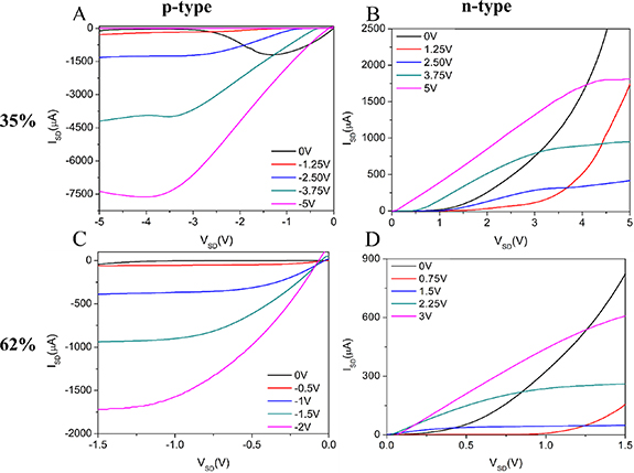
Figure 3. Output curves for SWCNT based TFTs operated in p-type (a) and (c) and n-type (b) and (d) using P(METATFSI-MMA) random copolymer PILs with 35 mol% (a) and (b) and 62 mol% (c) and (d) ionic repeat units, as the dielectric. The output curves themselves are all measured at 10 Hz.
Download figure:
Standard image High-resolution imageTo further probe the PIL dielectric characteristics, we characterised the devices at different voltage sweep rates which can be expressed as different operating frequencies and are reported in the corresponding transfer curves of figures 4 and 5. The voltage sweep rate frequency is determined by increasing the on/off delay of each voltage step. For example, f(Hz) = 1000/(ontime + offtime) ms. Therefore a 10 Hz voltage sweep rate would have an on time of 80 ms and an off time of 20 ms. For this analysis, the various frequencies match the colour of the dotted lines from figure 2. Table 1 highlights the n-type performance of devices fabricated using the 35 mol% and 62 mol% PILs and voltage sweep rates of 0.1, 10 and 100 Hz. The transfer curves for figures 4(a)–(c) were calculated using a SD voltage of −1 V For the devices made with 35 mol% PIL, as the frequency increases, we see an increase in the hysteresis. At frequencies greater than 10 Hz, the data becomes unreliable due to the large hysteresis values (figures 4(b) and (c)). The speed at which the EDL can be formed, as well as the corresponding mobility of the TFSI− anion and the respective PIL cation in devices are the leading factors for the observed hysteresis in PIL gated transistors [56, 57]. Further, examples in literature demonstrate that when using ionic liquids with SWCNTs and a fully formed EDL the hysteresis is greatly reduced [58, 59]. For the devices fabricated using 35 mol% PIL, this hysteresis can be attributed to the low ionic conductivity and the devices never fully reaching the EDL formation phase [60, 61]. As the characterization frequency is decreased, the TFSI− anions have more time to diffuse through the PIL bulk, leading to a reduction in hysteresis, until 0.1 Hz where the hysteresis becomes negligible as seen in figure 4(a). For devices fabricated using 62 mol% PIL, a much lower hysteresis is observed at almost all operating frequencies due to the greater ionic conductivity, allowing the 62% sample to reach the EDL formation phase at a higher frequency (figure 4(d)–(f)). These results are consistent with the capacitor results which demonstrate that 62 mol% PIL is in the EDL formation phase between 0.1 and 1 Hz compared to the 35 mol% PIL based capacitors which only begin to transition towards EDL formation at 0.1 Hz and is in the ionic relaxation phase for frequencies larger than 0.1 Hz [18]. For both PILs, reducing the frequency generally leads to an increase in transconductance which is a result of greater capacitance values [62]. The outlier occurred when using 35 mol% PIL sample at 10 Hz, which saw a decrease in transconductance. This decrease can be attributed to the low conductivity of 35 mol% sample [63]. Further, none of the samples operated above 0.1 Hz are within the EDL formation phase, increasing the variability on the measurements and highlighting the importance of selecting the proper operating frequency for PIL gated TFTs. When operating in the ionic relaxation region, the ionic displacement current caused by the diffusion of the TFSI− anions will impact device performance and variability [64]. The measured n-type gm at 0.1 Hz is 85 μS and 90 μS for devices fabricated using 35 mol% and 62 mol% PIL samples. Within literature n-type transconductances for SWCNTs have been reported to be 10–25 μS at room temperature [65, 66]. The values we obtained are approximately three times larger than the previously reported n-type devices [65, 66]. Furthermore, these results were obtained in air, demonstrating that the P(METATFSI-MMA) structure enables better encapsulation properties compared to PMMA and the operation of n-type SWCNT transistor devices under ambient conditions. This is uncommon for SWCNTs which are reported as ambipolar but need to be characterized under vacuum, in the absence of oxygen, to show significant electron transport and n-type behaviour [36, 42]. This is consistent with reports from Li Zhou who demonstrated air stability of n-type SWCNT transistors when using ion gels based on PS2-block-PMMA block copolymers with 1-Ethyl-3-methylimidazolium (EMIM)+ TFSI− as the dielectric [65].

Figure 4. Transfer curves for SWCNT based TFTs V SD = 0.5 V for the 35 and 62 mol% sample, operated in n-type using P(DMAEMA-TFSI-ran-MMA) random copolymer PILs with 35 mol% (a)–(c) and 62 mol% (d)–(f) METATFSI molar composition, as the dielectric. The transfer curves are operated at 0.1 (a) and (d), 10 (b) and (e) and 100 Hz (c) and (f). All transfer curves are plotted on a log scale.
Download figure:
Standard image High-resolution image
Figure 5. Transfer curves for SWNT based TFTs, VSD = −0.5 V, operated in p-type using P(METATFSI-MMA) random copolymer PILs with 35 mol% (a)–(c) and 62 mol% (d)–(f) ionic repeat units, as the dielectric. The transfer curves are operated at 0.1 (a) and (d), 10 (b) and (e) and 100 Hz (c) and (f). All transfer curves are plotted on a log scale.
Download figure:
Standard image High-resolution image
Table 1. Device characteristics of SWCNT based TFTs operated under n-type conditions at different operating frequencies.
| Dielectric | Frequency (Hz) |
H
|
IOn/off
|
gm
|
VT
| SS |
|---|---|---|---|---|---|---|
| 35 mol% | 0.1 | 0.09 ± 0.06 | 10^4 | 85 ± 16 | 1.6 ± 0.5 | 0.16 ± 0.04 |
| 10 | 1.7 ± 1.7 | 10^3 | 12.6 ± 14.8 | 2.7 ± 0.6 | 0.31 ± 0.25 | |
| 100 | 16.2 ± 18.5 | 10^4 | 53.1 ± 20.8 | 2.2 ± 0.3 | 0.27 ± 0.16 | |
| 62 mol% | 0.1 | 0.2 ± 0.1 | 10^3 | 90.9 ± 26.2 | 1.1 ± 0.1 | 0.14 ± 0.07 |
| 10 | 0.1 ± 0.1 | 10^2 | 44.2 ± 7.7 | 1.5 ± 0.1 | 0.13 ± 0.12 | |
| 100 | 0.1 ± 0.1 | 10^3 | 38.2 ± 19.5 | 1.2 ± 0.1 | 0.15 ± 0.10 |
a Dielectric: P(METATFSI-MMA) random copolymer PILs with 35 mol% and 62 mol% ionic repeat units. b Hysteresis, H, the on and off current ratio, IOn/off, the transconductance gm (μS) normalized for channel length, VT, subthreshold swing SS. c Large variabilities in hysteresis observed in experimental data when operated at high frequency.
The same devices were characterized under negative voltage (p-type operation), causing the corresponding TFSI− anions to diffuse into the SWCNT semiconductive layer (figure 1(b)). The smaller TFSI− anions can migrate and interact closely with the SWCNTs, causing the device to function similar to OECTs [16]. The devices fabricated using 35 mol% PIL as dielectric demonstrated a similar trend to the n-type devices where decreasing the operating frequency leads to a decrease in device hysteresis (table 2). The hysteresis for the devices operated at 10 Hz and 100 Hz for the 35 mol% PILs displayed large variability. The increase hysteresis with increasing frequencies is dominated by the sluggish frequency-capacitance response and the TFSI− anions doping the SWCNTs [67–69]. However, a large increase in hysteresis is not observed for devices fabricated using the 62 mol% PIL as dielectric as seen in both table 2 and figure 5. Therefore, we surmise the hysteresis is a result of the lower ionic conductivity of the 35 mol% PIL. Panzer et al have further demonstrated the impact of ion conductivity by reporting changes in hysteresis based on operating frequency, which they attribute to slow ion migration [70]. Within table 2 we see a similar trend to table 1 with an increase in transconductance as the frequency is decreased. We also observe a greater overall transconductance and greater on-current for the p-type operation compared to the n-type operation, which is consistent with the operation of OECTs where the TFSI− anions enhance the p-doping and hole conductivity of the fabricated TFTs [16, 40, 71]. Table 2 also shows a large variability for the hysteresis, and transconductance, which is most likely caused by the interactions between the TFSI− anions and the SWCNTs, and further amplified at higher frequencies due to the devices being in either the ionic or dipolar relaxation phase. The p-type devices also demonstrate greater on/off current ratios of 105 for both devices fabricated with the 35 mol% and 62 mol% PILs as dielectrics at 0.1 Hz (table 2) compared to the n-type TFTs which have on/off current ratios of 104 and 103 for the same PILs, respectively. This is also to be expected as OECTs enable greater currents and larger on/off current ratios in general [72]. The slightly lower on/off current ratio at 10 Hz for the 35 mol% sample is an indication of that PIL entering the ionic relaxation regime where ionic displacement currents decrease the on/off ratio [64]. These results demonstrate that P(METATFSI-MMA) random copolymer PILs used as dielectrics enable low voltage, high performance, air-stable ambipolar transistors. By tuning the copolymer composition, we can achieve large operating frequencies, high transconductance with low hysteresis.
Table 2. Device characteristics of SWNT based TFTs operated in p-type at different operating frequencies.
| Dielectric | Frequency (Hz) |
H
|
IOn/off
|
gm
|
VT
| SS |
|---|---|---|---|---|---|---|
| 35 mol% | 0.1 | 0.5 ± 0.5 | 10^5 | 48.5 ± 36 | −1.7 ± 1.0 | 0.25 ± 0.13 |
| 10 | 8 ± 25 | 10^4 | 25.6 ± 12.0 | −1.9 ± 0.8 | 0.26 ± 0.13 | |
| 100 | 14 ± 77 | 10^5 | 39.7 ± 12.6 | −1.5 ± 0.5 | 0.21 ± 0.11 | |
| 62 mol% | 0.1 | 0.3 ± 0.4 | 10^5 | 235.2 ± 144.4 | −0.9 ± 0.8 | 0.18 ± 0.09 |
| 10 | 0.03 ± 0.03 | 10^4 | 77.8 ± 24.1 | −0.6 ± 0.5 | 0.11 ± 0.07 | |
| 100 | 0.1 ± 0.1 | 10^4 | 94.1 ± 31.2 | −0.5 ± 0.2 | 0.12 ± 0.04 |
a Dielectric: P(METATFSI-MMA) random copolymer PILs with 35 mol% and 62 mol% ionic repeat units. b Hysteresis, H, the on and off current ratio, IOn/off, the transconductance gm (μS) normalized for channel length, VT, subthreshold swing SS. c Large variabilities in hysteresis observed in experimental data when operated at high frequency.
4. Conclusion
High capacitance PIL that allow for p- and n-type operation of SWCNTs under ambient conditions were successfully fabricated. Using both the 35 and 62 mol% PIL it was possible to analyse the impact of TFSI− anion doping on SWCNT performance when switching the devices from n- to p-type operation. The p-type devices demonstrated a higher transconductance and large on/off ratios, which is standard for OECTs. Next, the frequency dependence of the fabricated TFTs was tested at 0.1, 10 and 100 Hz. The fabricated devices showed a decrease in hysteresis with decreased frequency. Further, an increase in mol% of the METATFSI chain was also shown to increase conductivity and improve device performance by increasing the frequency at which the EDL formation phase begins. The simple synthesis of P(METATFSI-MMA) allowed for the investigation of the impacts of operating frequency and ionic repeat unit mol% in high performance SWCNT TFTs.
Acknowledgments
This work was supported by the NSERC Green Electronics Network (GreEN) (Grant No. NETGP 508526-17 to B H L), NSERC Discovery Grant (RGPIN-2020-04079 to B H L) and NSERC CGS to M T.
Data availability statement
The data that support the findings of this study are available upon reasonable request from the authors.
Supplementary data (1.6 MB DOCX)