

Abstract
The Schottky contact, formed at the interface between a metal and a semiconductor, is instrumental in defining the electrical properties of Schottky barrier diodes (SBDs). The characteristics of the Schottky contact are contingent on the properties of interacting metal and semiconductor properties. Herein, we studied the carrier-transport mechanisms and electrical characteristics at room and elevated temperatures. These SBDs employ pre-treated Ga2O3 thin films and either Ni or Au Schottky contacts. The SBDs pre-treated (pre-T) via annealing at 900 °C under an N2 atmosphere for the Ni contact showed highest on/off ratio at room temperature. They also demonstrated ideality factors and Schottky barrier heights (SBHs) that remained relatively stable between 298 K and 523 K. To ascertain the SBH, ideality factors (n) derived from the thermionic emission (TE) and thermionic field emission (TFE) models were used, and results were subsequently compared. Moreover, SBDs employing Ni as the anode material exhibited lower SBHs than those employing Au. The pre-T Ni SBD was best described by the TFE model, wherein the SBH and ideality factor varied by 0.14 eV and 0.13, respectively, between 298 K and 523 K. Conversely, for pre-T Au, untreated Ni, and untreated Au SBDs, neither TE and TFE provided a satisfactory fit due to the ideality factor is greater than 2 at room temperature and the variation of SBH and n with temperature. These suggests that the transport mechanism should be described by other physical mechanisms. Without pre-treatment, both the Ni and Au SBDs exhibited more significant variation in the SBH and n with temperature. SBHs values were determined using measurement of current, capacitance and x-ray photoelectron spectroscopy, and were found to depend on the interface quality, indicating inhomogeneous SBH. Our results suggest that the use of annealing pre-treatments and anode metals with low work functions holds considerable potential for reducing Schottky barrier heights in Schottky diodes, thereby enhancing their electrical performance.
Export citation and abstract BibTeX RIS

Original content from this work may be used under the terms of the Creative Commons Attribution 4.0 licence. Any further distribution of this work must maintain attribution to the author(s) and the title of the work, journal citation and DOI.
1. Introduction
In the electronics industry, metal–semiconductor (M–S) contacts are widely used to rectify electrical characteristics [1]. Among the devices employing the M–S structure, such as metal–semiconductor field-effect transistors and Schottky barrier diodes (SBDs), SBDs have the simplest device structures. Therefore, SBDs can be fabricated easily and are ideal for confirming the interfacial properties of the M–S contact. SBDs based on wide-bandgap materials have been investigated for power electronics applications. In the last decade, silicon carbide (SiC) and gallium nitride (GaN), which exhibit larger critical electric fields than conventional silicon, have been commercialized [2, 3]. Gallium oxide (Ga2O3) has drawn significant attention in power applications, owing to its higher switching efficiency and power-conversion density [4–6]. Ga2O3 has an ultra-wide bandgap in the range 4.7 eV to 5.2 eV [7–9] and a high theoretical breakdown field of 8 MV cm−1, which, in turn, attributes a large Baliga's figure of merit to it for power devices [10, 11]. For developing devices based on Ga2O3, the mechanisms underlying its electrical properties must be understood. The M–S interface plays a pivotal role in SBDs, and the Schottky barrier height (SBH) controls their electrical properties such as carrier-transport [12]. SBH can be predicted using the Schottky–Mott relation, which predicts that the SBH is equal to the difference between the electron affinity of the semiconductor and the work function of the metal [13]. However, experimentally, the SBHs predicted using the Schottky–Mott model are largely incorrect [14]. The temperature dependence of electrical properties elucidates various aspects of conduction mechanisms and determine the probability of spatial inhomogeneities at the M–S contact [15]. While there have been a few studies on the electrical properties of Ga2O3 SBDs [16, 17], they have focused on those with homogenous structures. Ga2O3 devices must employ heterostructure in combination with a material exhibiting good thermal characteristics such as SiC (280 W m−1 K−1) [18], to improve the poor thermal characteristics of Ga2O3 (10–29 W m−1·K−1) [19, 20]. In this study, we systematically investigated the M–S interface of Ga2O3/4H-SiC SBDs employing Ni or Au anode metals and Ga2O3 pre-treatments. The electrical properties were analyzed using current and capacitance characteristics. To understand the Schottky contact and carrier-transport mechanisms, temperature-dependent current–voltage characteristics were studied using thermionic emission (TE) and thermionic field emission (TFE) models. In addition, the values of SBHs were confirmed via x-ray photoelectron spectroscopy (XPS).
2. Experimental
In this study, a Ga2O3 thin film was deposited on n-type 4H-SiC substrates. Commercial 4H-SiC wafers from SK Siltron CSS 4 were used as-received. The n-type 4H-SiC wafers were doped at a concentration of 1 × 1019 cm−3 and had an epitaxial layer, with a nitrogen dopant concentration of 5 × 1016 cm−3, grown on them. The wafer was then cleaned using acetone, methanol, and deionized water for 15 min. Subsequently, acid cleaning was sequentially performed on it using a sulfuric acid–peroxide mixture (H2SO4:H2O2 = 4:1) for 5 min, followed by washing in deionized water for 10 min. Prior to the front-side processing of the sample, a large area of back-side contact was fabricated. For the cathode, Ni was deposited on the backside of the wafer using an electron beam evaporator. The fabricated devices were annealed at 1050 °C for 1 min in a rapid thermal annealing furnace under an N2 atmosphere to improve their abilities as Ohmic contacts. The Ga2O3 thin film was deposited on the epitaxial side of the wafer from a pure 99.99% Ga2O3 target, using a radio frequency magnetron sputtering system. A vacuum chamber was initially evacuated to a base pressure of 0.86 μPa and then purged with pure argon at 3.33 Pa for the duration of film deposition. The deposition was performed at a power of 120 W for 5 h, and the thickness of the deposited film was confirmed to be 300 nm via ellipsometry. The fabricated SBDs were divided into four groups: two of them were annealed in a tube quartz furnace at 900 °C under an N2 atmosphere for 1 h referred as pre-treatment (pre-T), and the other two were used without pre-treatment (w/o pre-T) for comparison. Subsequently, Schottky contacts were formed via thermal evaporation using 5N-purity metals as the sources, using a shadow mask with various diameter (1 mm, 0.75 mm, 0.5 mm, and 0.25 nm). Ni was deposited on the wafers belonging to one pre-T and w/o pre-T group each, and Au was deposited on the remaining two.
The Schottky contacts were characterized using current–voltage measurements, in the temperature range 298 K to 523 K and steps of 25 K in the dark. Electrical characterization was performed using a Keithley 4200 parameter analyzer in the dark. The interface of the metal and semiconductor was investigated using a Thermo Fisher Scientific K-Alpha XPS with an Al Kα x-ray (hν = 1486.6 eV) source. The samples were analyzed after the surface was etched with 200 eV of Ar+-ion bombardment for 90 s. XPS was performed on a 0.12 mm2 area at a pressure of 0.48 μPa. All XPS spectra were calibrated by the C 1s peak (284.6 eV) to compensate for a possible residual-charge effect.
3. Results and discussion
The current-density–voltage (J–V) characteristics and calculated specific on resistance (Ron,sp) values of the Ga2O3 SBDs at room temperature are shown in figure 1. These characteristics were measured by grounding the cathode, while the anode bias was increased from −3 V to 5 V, in steps of 0.01 V, and the current density was normalized to the anode Schottky area. The pre-T SBDs exhibited a higher on/off ratio than the w/o pre-T SBDs. Among the pre-T SBDs, the SBD with a Ni anode exhibited a higher on/off ratio than that with an Au anode. The values of Ron,sp for the w/o pre-T Ni and Au SBDs were determined to be 145 kΩ·cm2 and 356 kΩ·cm2, respectively, while those for pre-T Ni and Au SBD were determined to be 0.2 kΩ·cm2 and 10.7 kΩ·cm2, respectively, extrapolated at a current density of 5 A cm−2. Based on the TE model for an ideal Schottky diode [20, 21], the J–V characteristics were determined using equation (1).

where

Here, 


 and
and  represent the saturation current density, electric charge, ideality factor, Boltzmann constant, measurement temperature, Richardson's constant, and SBH, respectively. The theoretical value of
  was assumed to be 41 A cm−2K−2 [22], and the
  values were determined to be 1.08 eV, 1.15 eV, 1.02 eV, and 1.11 eV in the w/o pre-T Ni, w/o pre-T Au, pre-T Ni, and pre-T Au SBDs, respectively. The pre-T SBDs exhibited lower
  values, which was attributed to an increase in the affinity of Ga2O3 after annealing, as reported previously [19]. The
  values of Ni SBDs were lower than those of Au SBDs, owing to a larger work function of Au (5.22 eV) [23] than Ni (5.1 eV) [24]. The accuracy of a
  value obtained via TE depends on the corresponding value of the ideality factor,
  and is higher for
  values closer to unity [25]. However, in our case, the values of
  obtained using the TE model were 2.26, 2.84, 1.01, and 1.17 for the w/o pre-T Ni, w/o pre-T Au, pre-T Ni, and pre-T Au SBDs, respectively. Therefore, the obtained
  values may have been underestimated. To determine the
  values more precisely, the C–V characteristics were obtained for the SBDs, as shown in figure 2. When a voltage is applied across a metal–semiconductor interface in the reverse bias, the depletion region widens [26], which can be expressed by the depletion approximation, as follows:

where 
 and
and  represent the conduction band minimum, Fermi level, relative permittivity, vacuum dielectric constant, and doping concentration, respectively. With a relative permittivity of
  [27] for Ga2O3 and an electron effective mass of 0.27 m* [28], the
  values of w/o pre-T Ni and Au SBDs were found to be 2.24 eV and 3.02 eV, respectively. Furthermore, the
  values of pre-T Ni and Au SBDs were determined to be 1.21 eV and 2.29 eV, respectively. Thus, all
  values obtained from the C–V method were higher than those obtained using the TE model, which may be attributed to the Schottky barrier inhomogeneity [29–31]. The I–V method may have afforded localized low SBH values for current conduction [32]. In contrast, using the C–V characteristics, average SBH values were obtained [33]. Therefore, inhomogeneous SBHs were predicted in the SBDs. To investigate the electrical properties of the devices in detail, we conducted J–V measurements at various temperatures ranging from 273 K to 523 K, in steps of 25 K, for the Ga2O3 Schottky diodes. The I–V–T characteristics were expressed using the ideal TE model:


Figure 1. J–V characteristics measured at room temperature and extracted Ron,sp of the vertical Ga2O3 Schottky barrier diodes.
Download figure:
Standard image High-resolution image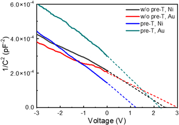
Figure 2. 1/C2–V characteristics of vertical Ga2O3 Schottky devices for the calculation of Schottky barrier heights. All Schottky barrier diodes were evaluated at 1 MHz.
Download figure:
Standard image High-resolution imageIn figures 3(a) and (b) respectively illustrate Richardson's plot for SBDs with and without pre-treatment. These plots are presented in different way: one adheres to the conventional method, while the other utilizes a modified approach that incorporates a temperature-dependent ideality factor. The slope of the straight line corresponds to the zero-bias barrier-height, denoted as intercept  As depicted in figure 3(a), the slope of graph, which associated with barrier height, varies significantly different metals in both of Richardson's plot. Conversely, the
  of pre-T SBDs are similar when viewed in modified Richardson's plot as demonstrated in figure 3(b). The values of
  and
and  were subsequently determined and are shown in table 1. The values of
  obtained for all devices using the conventional Richardson's plot differed significantly from the theoretical Richardson constant of Ga2O3, which is 41 A cm−2K−2 [21]. The conventional Richardson's plot does not account for the temperature dependence of ideality factors owing to the presence of interface states, image force, and surface charging [30, 32, 33]. To account for temperature-dependent ideality factors, the modified Richardson' plot was proposed by Hackam and Harrow, wherein the X axis represents 1 n−1k−1T−1 [33, 35]. Using the modified Richardson's plot, the Richardson constant for the pre-T Ni SBD was found to be 42.68 A cm−2K−2, which is comparable with the value obtained from the conventional Richardson's plot. The temperature-dependent ideality factors indicated carrier-transport mechanisms other than TE. The TFE model may be the other dominant carrier-transport mechanism in SBD devices [31, 36, 37]. In TFE, the carrier is tunneled through the potential barrier from the interface, and the I–V characteristics can be given by

where


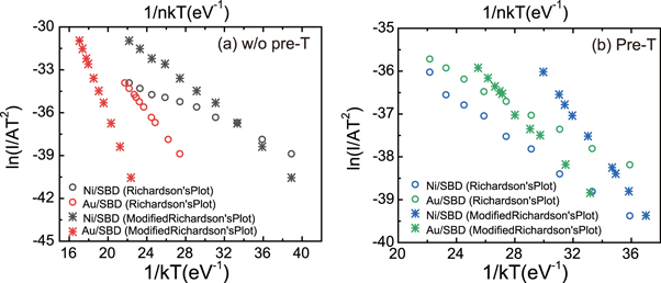
Figure 3. Conventional Richardson's plots of ln (I A−1T−2) versus 1 k−1T−1 and the modified Richardson's plot of In (I A−1T−2) versus 1 n−1k−1T−1. The Richardson's plots of w/o pre-T and pre-T SBDs are shown in (a) and (b), respectively.
Download figure:
Standard image High-resolution imageTable 1. Values of the Richardson constant and Schottky barrier height, as obtained from Richardson's plot.
| Richardson constant | Schottky barrier height (eV) | |||
|---|---|---|---|---|
| Conventional | Modified | Conventional | Modified | |
| W/o pre-T Ni SBDs | 3.26 × 10⁻⁶ | 28.31 | 0.57 | 0.94 |
| W/o pre-T Au SBDs | 1.08 × 10⁻⁷ | 13.26 | 1.03 | 1.81 |
| Pre-T Ni SBDs | 6.68 | 42.68 | 0.67 | 1.02 |
| Pre-T Au SBDs | 12.18 | 29.41 | 0.45 | 1.014 |
Here,  is the energy difference between the conduction band minimum and the fermi level, which can be expressed as
  where
where  is the effective density of states in the conduction band and
  is the carrier concentration.
  is the characteristic tunneling energy, which indicates the contribution of tunnel transmission. These tunneling current may be associated with several factors, including the quality of MS contact, interface quality between Ga2O3 and 4H-SiC, and the presence of defects within Ga2O3 and 4H-SiC. The E00 k−1T−1 and E0 k−1T−1 values of all devices obtained using the TFE model are given in table 2. The effectiveness of the TFE model can be predicted using the value of E00 k−1T−1. Notably, TFE becomes effective when E00 k−1T−1
 1 [35, 38]. When E00 k−1T−1
 1, the TE model is predominant, whereas FE is dominant when E00 k−1T−1
 1, because the tunneling probability of FE decreases more rapidly than that of TE. Therefore, the predominant carrier-transport mechanism in the pre-T Ni SBD may be TFE, because its value E00 k−1T−1 is the closest to 1.
Table 2. Electrical parameters of the Ga2O3 SBDs obtained experimentally, using the TFE model.
| W/o pre-T Ni SBD | W/o pre-T Au SBD | Pre-T Ni SBD | Pre-T Au SBD | |||||
|---|---|---|---|---|---|---|---|---|
| Temp (K) | E00 k−1T−1 | E0 k−1T−1 | E00 k−1T−1 | E0 k−1T−1 | E00 k−1T−1 | E0 k−1T−1 | E00 k−1T−1 | E0 k−1T−1 |
| 298 | 2.13 | 2.42 | 4.68 | 4.73 | 1.15 | 2.16 | 2.21 | 2.64 |
| 328 | 2.02 | 2.28 | 4.64 | 4.45 | 1.13 | 1.98 | 2.08 | 2.71 |
| 353 | 1.96 | 2.10 | 4.37 | 4.43 | 1.08 | 1.85 | 2.00 | 2.63 |
| 378 | 1.92 | 1.88 | 4.22 | 4.34 | 1.03 | 1.75 | 1.96 | 1.96 |
| 403 | 1.86 | 1.76 | 4.12 | 4.41 | 1.01 | 1.66 | 1.92 | 1.66 |
| 428 | 1.86 | 1.30 | 4.05 | 4.20 | 1.00 | 1.58 | 1.90 | 1.52 |
| 453 | 1.85 | 1.15 | 3.93 | 4.12 | 0.98 | 1.51 | 1.86 | 1.37 |
| 478 | 1.83 | 0.98 | 3.82 | 4.01 | 0.95 | 1.45 | 1.84 | 1.31 |
| 503 | 1.77 | 0.95 | 3.71 | 3.89 | 0.93 | 1.40 | 1.77 | 1.51 |
| 528 | 1.79 | 0.91 | 3.58 | 3.83 | 0.93 | 1.35 | 1.75 | 1.50 |
To further confirm the carrier-transport mechanism, the temperature dependence of  and
and  was analyzed using the TE and TFE models, as shown in figure 4. With increasing device temperature, most of the devices showed
  increased and
  decreased, and the values obtained using both models showed the same trend. The temperature dependent barrier height and ideality factor are generally attribute to the inhomogeneous barrier height in Schottky contact [15]. An increase in the value of
  with temperature was attributed to an increase in the thermal energy of the electrons, which enabled them to cross higher barriers. As a result, the dominant barrier height will increase with the temperature and ideality factor could be expected to decrease. As shown in figures 4(c) and (d), the
  values obtained using the TFE model lay in the ranges 1.40 eV to 1.54 eV and 1.61 eV to 1.79 eV, from 298 K to 523 K, in the w/o pre-T Ni SBD and w/o pre-T Au SBD, respectively. Meanwhile, the
  values obtained using the TE model ranged 1.03 eV to 1.46 eV and 1.11 eV to 1.46 eV, from 298 K to 523 K, in the pre-T Ni and Au SBDs, respectively. This indicates that the TFE model may be more effective for carrier-transport in pre-T SBDs than the TE model, particularly the pre-T Ni SBD, whose E00 k−1T−1 ratio was closest to unity, as previously mentioned. However, the
  values of w/o pre-T SBDs varied significantly with temperature, which could be attributed to the dominance of the non-ideal effect, such as an inhomogeneous
  or trap-assisted tunneling current and interface quality [18]. The ideality factor value exceeding unity may be attributed to various factors, including the quality of interface states between metal and semiconductor, as well as the presence of tunneling currents. The Au SBDs exhibited an
  value that was greater than unity, which could be attributed to other carrier-transport mechanisms.
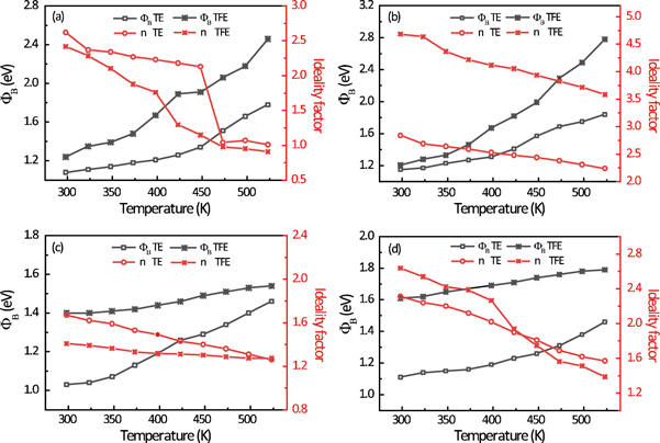
Figure 4. Temperature dependence of Schottky barrier heights and ideality factors obtained from the TE and TFE models in the (a) w/o pre-T Ni, (b) w/o pre-T Au, (c) pre-T Ni, and (d) pre-T Au Schottky barrier diodes.
Download figure:
Standard image High-resolution imageIn figure 5, XPS analysis was performed to confirm the surface composition and band alignment at the interface of the anode and Ga2O3. The XPS results indicated a composition of 53 to 51% oxygen and 47% to 45% gallium, suggesting that the epitaxial film is oxygen-deficient. And coming to the Ga 3d spectra, Ga 2+ is approximately 11% of all the Ga atoms which indicates that supporting sub-stoichiometric oxide composition as shown in figure S1. The barrier potential  was then calculated using the subsequent equation, as described in references [39, 40]:

here  is the energy bandgap of Ga2O3,
  is the valence-band maximum binding energy, and
  and
and  are the core levels of bulk Ga2O3 and anode/Ga2O3 interfaces, respectively.
  was estimated using the energy-loss peak of the O 1s spectrum [41–43] and was equal to the difference between the peak of O 1s and the onset of inelastic losses. Thus,
  was determined to be 4.90 eV and 4.79 eV in the w/o pre-T and pre-T SBDs, respectively. As shown in figures 5(d) and (e),
  is a constant related to material characteristics, the values of which were found to be 1114.7 eV and 1114.3 eV, using XPS, for the Ga2O3 films of w/o pre-T and pre-T SBDs, respectively. The binding energies of Ga 2p corresponding to the metal/Ga2O3 interfaces,
  for the w/o pre-T Ni, w/o pre-T Au, pre-T Ni, and pre-T Au SBDs were 1118.31 eV, 1118.11 eV, 1117.96 eV, and 1117.71 eV, respectively. Furthermore, using equation (8), the
  values of the SBDs were calculated to be 1.29 eV, 1.49 eV, 1.13 eV, and 1.38 eV, respectively. These
  values of w/o pre-T SBDs were greater than those obtained from TFE, while the values of pre-T SBDs were intermediate between those derived from the TE and TFE models. To understand the
  in the energy band diagram is shown in the figure 5(f). These
  values of w/o pre-T SBDs were greater than those obtained from TFE, while the values of pre-T SBDs were intermediate between those derived from the TE and TFE models. Figure 6 shows the summary of the SBH with the research results in the literature. The Schottky–Mott relation represented with dashed line is rarely observed although the prior studied Ga2O3 SBDs. The SBDs with Ni metal, the values of SBH from different methods are similar except w/o pre-T SBDs. However, the SBHs are quite different depending on methods to obtain in w/o pre-T SBDs. Inhere, the SBDs also not only varies on metal work function, but orientation, surface, pretreatments of Ga2O3. The SBDs with Au anode have a universal trend with the different Ga2O3 surface, indicating that the interface states with Au metal are inhomogeneous with defect.
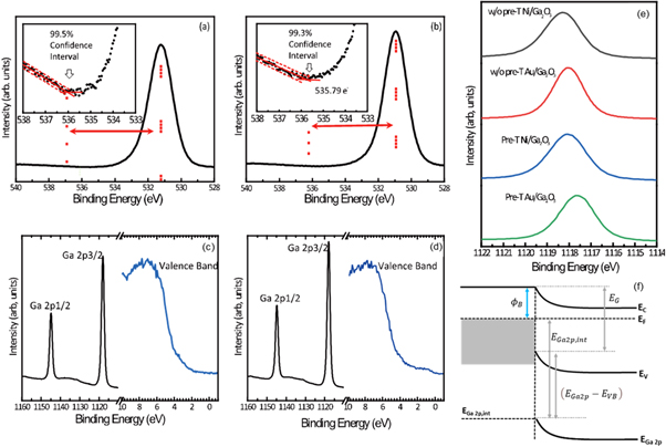
Figure 5. XPS O 1s core-level spectra of (a) w/o pre-T and (b) pre-T Ga2O3 films to determine the bandgap of Ga2O3. (c) Band diagram of an ideal metal–semiconductor interface. Ga 2p core-level spectra and valence-band spectra of (d) w/o pre-T and (e) pre-T Ga2O3 films. (f) Ga 2p core level spectra of the interface between Ga2O3 and the metal for the four Schottky barrier diodes.
Download figure:
Standard image High-resolution image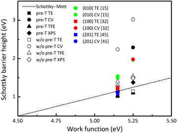
Figure 6. Dependence of the Schottky barrier height on the metal work function. The Schottky barrier heights have been determined using various methods: Thermionic Emission (TE, represented by squares), Capacitance-Voltage (CV, circles), Thermionic Field Emission (TFE, triangles), and x-ray Photoelectron Spectroscopy (XPS, diamonds). The experimental results are depicted in black and white. The metal work function values were considered from reference [44].
Download figure:
Standard image High-resolution image
4. Conclusions
This study evaluates the electrical properties of Ga2O3/4H-SiC SBDs and the effect of pre-treatment and various Schottky contacts on them. In forward bias, the Ron,sp values of pre-T SBDs are lower than those of w/o pre-T SBDs. The rectifying behavior of J–V characteristic measurements suggests that the junction between the metals and Ga2O3 exhibits a Schottky barrier. SBHs determined from J–V and C–V characteristics are different, which suggests the existence of inhomogeneous SBHs in SBDs. Furthermore, the SBHs and ideality factors of Schottky diodes are temperature dependent, which can be attributed to diverse carrier-transport mechanisms and spatially non-flat SBHs. By analyzing the temperature dependence of the I–V characteristics using the TE and TFE models, the values of the SBHs and ideality factors can be obtained. Carrier-transport in pre-T SBDs occurs predominantly via TFE, whereas that in w/o pre-T SBDs occurs predominantly via FE, as confirmed by E00 kT-1. SBDs pre-treated via annealing and employing anode metals with lower work functions exhibit lower SBHs. This indicates that the use of annealing pretreatments has significant potential for ideal carrier-transport mechanism and improving electric properties. Moreover, the Ni is appropriate for anode metal of Ga2O3 SBDs to obtain flat SBHs compared to Au.
Acknowledgments
This work was supported by Fostering Global Talents for Innovative Growth Program through KIAT (P0017308 and P0012451), SK Siltron and a Research Grant from Kwangwoon University in 2023. The authors thank Qiliang Li at George Mason University, USA and Sujitra Pookpanratana at National Institute of Standards and Technology (NIST), USA for allowing Research-Visit collaboration of graduate students.
Data availability statement
All data that support the findings of this study are included within the article (and any supplementary files).
Footnotes
- 4
Certain commercial equipment, instruments, or materials are identified in this paper in order to specify the experimental procedure adequately. Such identification is not intended to imply recommendation or endorsement by NIST, nor is it intended to imply that the materials or equipment identified are necessarily the best available for the purpose.
Supplementary data (0.1 MB DOCX)