
Abstract
Ferroelectric with quantum-mechanical tunnel allows non-volatile resistance states and fast readout of the tunnel current in the ferroelectric tunnel junctions (FTJs) through the influence of ferroic orders. However, the complex interfacial effect between electrodes and traditional ferroelectric films has still remained to be solved. When 2D ferroelectrics are used in FTJs, the lattice-matched constraint and intermixing of cations between ferroelectric and substrate electrode can be avoid. Here we show various FTJs with low energy consuming, and high endurance made from 2D ferroelectric ReS2 and different electrodes such as Pt/ReS2/Au, W/ReS2/SiO2/Si and W/ReS2/Nb:STO. With the help of in situ atomic force microscopy and piezoresponse force microscopy, we show that the memory can be manipulated in less than 1 μm2 and the resistance switching should be caused by the ferroelectric polarization direction in the distorted ReS2. Then, we demonstrate that the memory devices can be easily transferred to a polyimide or flexible SiO2/Si substrate. These FTJs shows good bending stability, illustrating their potential applications in flexible electronics. Considering the weak Van der Waals interfacial bonding between 2D ferroelectric and electrode, the polarization-dependent Schottky emission and interface-limited Fowler–Nordheim tunnel current play the key role in resistance switching respectively. Our work provides a simple way to construct various building blocks for circuits in harsh electronics with low energy consuming, good bending stability and high-density data storage.
Export citation and abstract BibTeX RIS

Original content from this work may be used under the terms of the Creative Commons Attribution 4.0 licence. Any further distribution of this work must maintain attribution to the author(s) and the title of the work, journal citation and DOI.
1. Introduction
Memristor is a promising candidate for future nonvolatile memory and bioinspired neuromorphic computing technologies for scalability, stability, multi-level switching, and CMOS compatibility [1–7]. The demand for low-operating-power [4], high-performance [8] and miniaturized devices [9–12] is rapidly growing in integrated circuits and internet of things industries. This motivates experimental and theoretical investigations into novel low-dimensional systems such as 2D layers [13–16], and single molecules [17]. Currently, memristor still suffers from the disadvantages of high current ratio of half voltage [18, 19]. Among these memristors, ferroelectric tunnel junction (FTJ) is an important candidate. A junction consisting of two electrodes separated by a nanometer-thick ferroelectric barrier which allows quantum-mechanical tunnel through it, is named as FTJ [7, 20–22]. The tunnel resistance of FTJ depends on the ferroelectric polarization direction which causes two degenerated resistance states ON and OFF. Based on the two degenerated ON/OFF states, the FTJ would offer high density of data storage, non-volatile resistance states, low energy consuming, and an easily scaled-down size [23–25]. Therefore, FTJ has recently aroused extensive attention for applications in memristor.
To maintain ferroelectric in traditional nanometer-thick perovskite thin films, sophisticated experimental approaches such as careful control of epitaxial growth in special substrates are generally required [22, 26]. Recently, ultrathin BaTiO3 ferroelectric film could be deposited or epitaxial grown on substrate of LaSrMnO3 or Nb:SrTiO3 (Nb:STO) to form FTJ device. These FTJ devices show excellent performance, such as large ON/OFF ratio, high density of data information and so on. But, the intermixing of cations at the interfaces between ferroelectric film and substrate can veritably lead to complicated variations of tunnel resistance. In 2D out-of plane ferroelectric layers, this interfacial effect can be greatly simplified for the weak Van der Waals interfacial bonding in the interface. And the 2D ferroelectrics can be easily transferred to different kinds of substrate electrodes to make different types of memristor for various application scenarios [22, 27]. The distorted structures of 2D ReS2 would break its in-plane inversion asymmetry and provide out-of-plane ferroelectric polarization in ReS2. Among the 2D ferroelectric materials, the distorted ReS2 is very stable and shows nice flexibility. Otherwise, the characteristics of distorted ReS2 changes little with the changing numbers of layer. Therefore, we made the FTJ devices based on 2D ferroelectric ReS2 nanosheets (∼20 nm thickness). All the FTJ based on different electrodes exhibit repeatable resistance switching with the similar coercive voltage, non-volatile resistance states, low-operating power and high data density. The most ON/OFF ratio of FTJ junctions reaches ∼10000% at room temperature. By combining piezoresponse force microscopy (PFM) with conductive-tip atomic force microscopy (CAFM), we demonstrated that the resistance switching is most probably caused by the reversal of ferroelectric domains. And the non-volatile resistance switching effect could be uniformly controlled in the size of less than 1 μm2 evenly. Finally, the mechanical flexibility of such memristor devices prepared on polyimide (PI) and flexible SiO2/Si substrate show good endurance against mechanical bending of hundreds of cycles.
2. Device fabrication and switching performance
Figure 1(a) shows the atomic force microscopy (AFM) image of the distorted ReS2 nanosheet. The ReS2 nanosheet is fairly flat with a less 0.84 nm thick terrace in figure S1(available online at stacks.iop.org/MRX/8/056301/mmedia). As we know Tc phase is centrosymmetric (orange dots, figure S2(a)) and Td phase is non-centrosymmetric (turquoise dots, figure S2(b)). Using spherical aberration corrected scanning transmission electron microscopy (Cs-corrected STEM), a series of transition structures (Tt) between the Tc and Td phases are identified in figure 1(b). And the ReS2 nanosheet keeps high crystallinity, according to the selected area electron diffraction (SAED) pattern along c axis in the inset of figure 1(b), and the X-ray diffraction (XRD) spectrum in figure S3. The Raman spectra of pristine Td phase and Tc ReS2 are shown in figure 1(c). Obviously, the Raman shift peak in 130.4 cm−1 doesn't exist in Td phase ReS2. As the extra peaks in 130.4 cm−1 only belonging to Tc phase [28], this peak could be used to identify the distribution of Tc and Td. Therefore, the distribution of all kinds of phases in ReS2 nanosheets could be acquired by mapping the Raman peak of 130.4 cm−1 in figure 1(d). According to the intensity of peaks 130.4 cm−1, we can clearly obtain the distribution of Tc and Td phase by the mapping of the intensity of 130.4 cm−1 in the synthesized ReS2, confirming their coexistence.

Figure 1. (a) AFM topographical image of a synthesized distorted ReS2 on a silicon wafer. (b) Cs-corrected STEM image of a distorted monolayer in which the Tc (orange balls), Td (cyan balls) and transition structures are observed clearly. The lattice interspacing of the zigzag chain in the transition structure shows a noticeable increase from 0.25 nm of Tc phase to 0.36 nm of Td phase (the bottom with shifty colors). Scale bar: 0.5 nm. The SAED pattern of the synthesized ReS2 showing the high crystallinity in inset. (c) The Raman spectrum of pristine Td phase (olive) and Tc phase (orange). (d) The distribution pattern of Tc (yellow) and Td (blue) phase, acquired by the distribution of the intensity of 130.4 cm−1.
Download figure:
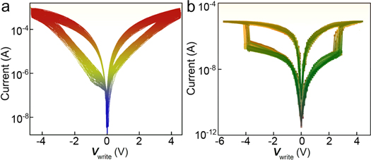
Standard image High-resolution imageTo measure the ferroelectric properties of the distorted ReS2 and the electric resistance response of the ReS2/Au junctions, we firstly carried out piezoresponse force microscopy (PFM) measurements to the top surface of distorted ReS2 (∼20 nm thickness) coated with Pt electrode. This can diminish the effect of charges absorbed on the surface of ReS2 nanosheets. The amplitude and phase hysteretic loops in the vertical PFM of the synthesized ReS2 are shown in figures 2(a) and (b). Obviously, the amplitude loop shows classical butterfly shape and the phase hysteresis shows the expected 180° phase contrasts. This phenomenon indicates the intrinsic ferroelectric in the synthesized ReS2. To investigate resistance switching in the ferroelectric devices in situ, electric contact was made through the AFM tip ( V write) to measure the tunnel current of the FTJ device. Figure 2(c) shows the tunnel current versus voltage of the FTJ based on ReS2 by conductive atomic force microscope. Obviously, the coercive voltages ( V C) for polarization reversal coincides with the voltages at which resistance switching occurs. At a negative V C of about—4.5 V, resistance switches from a high to a low value and the device is in the 'ON' state for polarization pointing upward (towards the Pt top electrode). Similarly, at a positive V C of about +3.5 V, the 'OFF' state is reached by switching the polarization downward (towards the Au bottom electrode). A clear large hysteretic variation of the resistance state with V write is also observed, and well-defined resistance switching occurs at the coercive voltage inferred from the PFM loops. We argue that the resistance switching should be caused by the reversal of ferroelectric polarization in the ReS2 FTJ junctions, although more complex resistance switching mechanisms involving electrochemical interface reactions cannot be completely excluded temporarily [19]. From figure 2(d) it is clear that both ON/OFF states are relatively stable for successive readouts in different junctions.

Figure 2. (a), (b) Out-of-plane PFM amplitude (a) and phase (b) measurements on a typical Pt/ReS2/Au ferroelectric tunnel junction. (c) Voltage dependences of the resistance switching of a Pt/ReS2/Au junction. (d) ON (olive) and OFF (orange) resistance states measured after applying 1 ms voltage pulses to 50 different junctions. Average OFF/ON ratio is 9 (range, 4–21).
Download figure:
Standard image High-resolution imageOwning to the preparation of 2D ferroelectric ReS2 without any lattice-matched constraint of the substrate, we then transferred the ReS2 nanosheets (∼20 nm thickness) to different substrate electrodes to verify the resistance switching observed above. Figure 3(a) shows the similar resistance switching observed in a W/ReS2/SiO2/Si FTJ device. The ON/OFF ratio of about ∼95 is much larger than the ratio (∼9) observed in Pt/ReS2/Au FTJ. This is because of the semiconducting electrode can effectively enlarge the tunnel barrier width with respect to metal electrodes, resulting in a larger ON/OFF ratio. In figure 3(b), typical binary resistance switching with good retention is also achieved. Both ON/OFF states can keep well at last 1500 s. And good reproducibility over 100 write/read cycles of the above FTJ is achieved in figure 3(c). The OFF and ON states are switched at poling voltages ± 5 V and the write power is as low as ∼5 × 10 3 A cm−2. And the poling voltages are coincided with the coercive voltages of the ferroelectric polarization. The similar resistance switching can be also achieved in the typical substrate electrode Nb:STO shown in figure 3(d). The retention and reproducibility of both OFF/ON states at poling voltages ± 5 V can also be kept well in figure 3(e) and figure 3(f). The reliable switching reproducibility, long data retention and low writing power observed in these metal/ferroelectric/semiconductor FTJs suggest their great potential in non-destructive readout non-volatile memories. Mostly, the similar resistance switching in FTJs with different substrate electrodes also verify that the resistance switching origins from the reversal of ferroelectric polarization. And the ReS2 nanosheets can be easily transferred to different substrates to form various FTJ devices, which can successfully solve the lattice-matched constraint between traditional ferroelectric films and substrates.

Figure 3. (a) Voltage dependences of the resistance switching in a W/ReS2/SiO2/Si FTJ. (b) The retention time of both ON (olive) and OFF (orange) states in a W/ReS2/SiO2/Si FTJ. The read voltage is Vread = 0.5 versus (c) Reversible binary resistance switching between ON (olive) and OFF (orange) resistance states by poling voltages ± 5 V in a W/ReS2/SiO2/Si FTJ. (d) Voltage dependences of the resistance switching in a W/ReS2/Nb:STO FTJ. (e) The retention time of both ON (olive) and OFF (orange) states in a W/ReS2/Nb:STO FTJ. The read voltage is Vread = 0.5 versus (f) Reversible binary resistance switching between ON (olive) and OFF (orange) resistance states by poling voltages ± 5 V in a W/ReS2/Nb:STO FTJ.
Download figure:
Standard image High-resolution imageCAFM is used to investigate the resistance switching effect in the FTJ device based on ReS2 [29–31]. The conductive path is patterned over the surface of ReS2 nanosheet in CAFM reading maps ( V read = 0.5 V) of the junction made from ReS2 with ∼20 nm in thickness (ReS2/Au) (figure 4a). After the poling voltage of ± 5 V in box-in-box patterns under reverse DC bias, we can switch the ON/OFF states in micro-region of the ReS2. The CAFM image obtained by the application of 0.5 V to CAFM tip (read voltage) is shown in figure 4b in situ The box-in-box pattern of ON and OFF states is quite in coincidence with its polarization reversal pattern with PFM in figure S5. Combining with the typical ferroelectric phase hysteresis and butterfly loops above, this resistance switching effect certainly originates from the ferroelectric of ReS2 nanosheet. The plots of ln( J/T 2) and E 1/2 of OFF state at positive bias in 150, 200 and 300 K are shown in figure 4c. The fitted linear curves and the corresponding calculated refractive indeices n [32–34] are shown in figure 4c, indicating the Schottky emission at high electric fields [35, 36]. The plots of ln( J / E 2) and (1/ E ) at negative bias in 150, 200 and 300 K is shown in figure 4d. The onset electric field obviously decreases with increasing temperature, indicating the conduction mechanism is mostly Fowler-Nordheim (FN) tunnel at high electric fields at negative bias [37–40].

Figure 4. (a) The conductive channel read by 0.5 V in the bare surface of layered ReS2 (2 × 2 μm2) on silicon coated with Au. (b) CAFM reading maps of the layered ReS2 (2 × 2 μm2) in situ after box-in-box voltage, demonstrating the polarization direction-dependent resistance in the junction of ReS2/Au. (c) ln( J/T 2) versus E 1/2 plots at positive biases in 150, 200, 300 K. (d) ln( J/E 2) versus 1/ E plots at negative biases in 150, 200, 300 K.
Download figure:
Standard image High-resolution imageWe fabricated flexible FTJs of Pt/ReS2/Au on PI substrate to detect the mechanical flexibility of the FTJ memristor. The flexible FTJ devices show typical resistance switching curves in figure 5(a). The FTJ device remains functional over 100 bending cycles with repeated mechanical bending to a radius of curvature of 1 cm on PI substrate [36]. The similar flexibility can also be observed in FTJ W/ReS2/SiO2/Si in figure 5(b). The typical bipolar resistance switching still maintains functional over 100 bending cycles with repeated mechanical bending to a radius of curvature of 5 cm on flexible SiO2/Si substrate electrode. These flexible FTJ memristors with low energy consuming are ideal for harsh electronics against mechanical stress and other flexible electronic applications.
Figure 5. Sustainability of bipolar resistance switching with repeated mechanical bending to (a) a radius of curvature of 1 cm on PI substrate and (b) a radius of curvature of 5 cm on flexible SiO2/Si substrate electrode.
Download figure:
Standard image High-resolution image
3. Conclusions
We fabricated flexible ferroelectric tunnel junction with bipolar resistance switching performance based on 2D ferroelectric ReS2. Without of the lattice-matched constraint, these ReS2 can be easily transferred to different kinds of substrate electrodes to form various FTJ devices such as Pt/ReS2/Au, W/ReS2/SiO2/Si and W/ReS2/Nb:STO. These kinds of FTJ memristors show low energy consuming, long retention time and high data storage density. As the ReS2 shows nice flexibility, the ReS2 are successfully prepared on various flexible substrate electrode forming different kinds of flexible FTJs. These FTJs show good flexibility and low energy consuming, which makes them the promising building blocks for the miniaturization and integration of memristors in harsh electronics. By CAFM and PFM measurements, we confirm that the resistance switching comes from the intrinsic reversal of ferroelectric polarization. If a 2D ferromagnetic ferroelectric or a multiferroic barrier is used, multi-states multiferroic tunnel devices or low-power electric-field-controllable spintronics may be realized in this one single micro-memory node.
Acknowledgments
This work is supported by Natural Science Foundation of Jiangsu Province (No. BK20190948) and National Natural Science Foundation of China (No. 61904119). This work was supported by the Natural Science Foundation of the Jiangsu Higher Education Institutions of China (17KJA140001), Six Talent Peaks Project of Jiangsu Province, China (XCL-078), and Jiangsu Key Disciplines of the Thirteenth Five-Year Plan (20168765). This work is also supported by PAPD, USTS Cooperative Innovation Centre, and Suzhou Key Laboratory for Low Dimensional Optoelectronic Materials and Devices (SZS201611). This work is supported by the Natural Science Foundation of the Jiangsu Higher Education Institutions of China (19KJB150018). Natural Science Foundation of Jiangsu Higher Education Institutions (18KJA470004).
Data availability statement
All data that support the findings of this study are included within the article (and any supplementary files).