
Abstract
This study proposes the High-κ dielectric Trench Shielded power UMOSFET (HK TS-UMOSFET) to be assessed using the two-dimensional numerical simulations. The simulations are employed to evaluate HK TS-UMOSFETs susceptibility to single-event burnout (SEB) mechanism. Based on the findings, the influence of alternative high permittivity gate dielectrics to silicon dioxide (SiO2) in TS-UMOSFET was discussed. Furthermore, in order to improve the performance of the device, its electrical behaviour was simulated with several high-κ dielectrics including Al2O3, Si3N4 and Aluminium Nitride (AlN). When heavy ions strike the sensitive areas of the device, the electric field distribution and SEB threshold values were extracted. Based on the values yielded, (AlN) was identified as a promising high-κ material to achieve SEB-hardened TS-UMOSFET compared to the other high-κ dielectrics. In conclusion, with (AlN), the HK TS-UMOSFET offers a high SEB tolerance and improved electrical characteristics.
Export citation and abstract BibTeX RIS

Original content from this work may be used under the terms of the Creative Commons Attribution 4.0 licence. Any further distribution of this work must maintain attribution to the author(s) and the title of the work, journal citation and DOI.
1. Introduction
High-frequency power switching systems usually prefer power MOSFETs, especially trench MOSFETs in space applications. However, its reliability is affected by the radiation effects induced by the energetic heavy ions in the radiation environment [1–3]. Among the destructive radiation effects is the Single-Event Effects (SEE), which is capable of permanently damaging the device. SEEs are classified into Single-Event Burnout (SEB) and Single-Event Gate Rupture (SEGR). SEB mainly depends on the inherent parasitic bipolar junction transistor (BJT) in the MOSFET structure. So, heavy-ions that pass through the power MOSFET during OFF state condition deposit charge along its ion track. The deposited charge then turns ON the parasitic BJT resulting in the high level of current due to the short between source and drain, which finally causes the device to burnout. The activation of the parasitic BJT is due to the interaction of the ionized space charge generated by the high energy ions along its trajectory through the device and the strong electric field in the depletion region of the reverse biased n/drift/substrate junction.
Furthermore, the Linear Energy Transfer (LET) is used to describe the amount of ionisation depending on the ion species and energy. Meanwhile, the geometry of the MOSFET elementary cells determines the shape of the electric field and the active volume of the parasitic transistor. When the ionisation column interacts with the high applied electric fields, a substantial amount of current passes along the space charge column. A drop in the voltage occurs when a fragment of the current runs laterally into the bulk. Voltage drop is determined by the bulk resistivity, where it may surpass the threshold value required to directly polarise (forward bias) the base-emitter junction (i.e. source-bulk) of the parasitic transistor. In the case of SEGR, the sensitive strike location is at the neck region i.e., centre of the device or area between p-body diffusions. It will then accumulate excessive holes at the Si−SiO2 interface causing a gate-oxide breakdown [4–6]. Therefore, this study focuses on the primary design concerns namely the suppression of the electric field density and the prevention of gate oxide damage in the enhancement of the trench MOSFET structure.
Previous literature has extensively investigated many potential hardening techniques to improve the SEE survivability of trench MOSFET which is also known as power U-shape Metal Oxide Semiconductor Field Effect Transistor (UMOSFET) [7–12]. Previous solutions are mainly focused on the Radiation Hardened by Design (RHBD) techniques to mitigate the radiation effects in UMOSFET. However, some researchers have assessed the Radiation Hardness by Process (RHBP) method for SEE hardening of Vertical Double Diffused Metal Oxide Semiconductor Field Effect Transistor (VDMOSFET). Wan et al proposed that Si3N4 is a promising gate dielectric to achieve SEB-hardened VDMOS [13]. In addition, [14] high-κ dielectric material for an inner dielectric layer (ILD) and passivation layer designs have been identified to significantly improved the Total Ionizing Dose (TID) and SEB performance of VDMOS. However, the effects of SEB on UMOSFETs using high-κ dielectric as a gate oxide has not been fully investigated and discussed.
Consistent with previous practice in VDMOS, this study also incorporated high-κ dielectric as a gate oxide on TS-UMOSFET to mitigate the SEB effects. In order to reduce the high electric field and ON-resistance, the n-type region was added to cover the P+ shielded region at the bottom of the trench. Besides that, different high-κ dielectric materials were used instead of SiO2 to prevent the gate oxide damage at the bottom of the trench. Hence, two-dimensional SEB simulations for the High-κ TS-UMOSFET and a structure with standard gate dielectric were performed using the Silvaco ATLAS simulator to compare the characteristics of the parameters. Finally, the SEB performance was investigated by analysing the inner physical behaviour, a critical value of LET and the safe operating voltage of the device during heavy-ion radiation. The simulation results indicated that high-κ dielectrics are promising techniques to achieve SEB hardened power TS-UMOSFET.
2. High-κ dielectrics on trench shielded power MOSFET
Figure 1 illustrates the schematic diagram of a standard power UMOSFET and High-κ Trench shielded UMOSFET with a breakdown voltage of 70 V. The width of the device's unit cell was 3.0 μm, while the channel length was 0 .4 μm. On the other hand, the electric field increases at the bottom of the trench corner when SEB occurs in a silicon UMOSFET. The addition of P+ shielding region below the trench bottom significantly reduces the high electric field. But, this P+ shielding region increases the ON-resistance due to the formation of JFET region. In order to reduce the resistance, n-region was added to cover the P+ shielding region. This structure spreads out the electrons to the bottom of the P+ shielding region conducting electrons in a downward direction [15–17]. Furthermore, a thinner gate oxide should be used to maintain the electrical characteristics with the addition of the shielding region. However, the standard (SiO2) gate oxide was unable to withstand a high electric field, resulting in the breakdown of the gate oxide. In order to prevent the gate oxide damages, a high-κ dielectric material is used instead of SiO2.

Figure 1. Schematic Diagram of (a) Power UMOSFET structure (b) High-κ TS-UMOSFET structure.
Download figure:
Standard image High-resolution imageIn contrast to standard UMOSFET, the HK TS-UMOSFET contains P+ shielding region surrounded by n-region with the thickness are set to 0.1 and 0.2 μm, respectively. The doping concentration of the layers were set at 1.0 × 1019 cm−3 and 6.0 × 1016 cm−3. In addition, the n-buffer layer was included to enhance the SEB performance [18]. The thickness of the drift region was reduced from 2.5 to 2.4μm in order to insert the buffer layer. The thickness of the buffer layer and doping concentration was set at 0.7 μm and 5.6 × 1016 cm−3, respectively. Table 1 summarises the device parameters used for the design simulation. Table 2 lists the various high-κ materials used in this study along with their physical properties. Since the dielectric constants for Al2O3, Si3N4 and AlN are higher than that of SiO2, the thickness of high-κ dielectric used for the simulation was calculated using equation (1).

where  high−κ and Thigh−κ are the dielectric constant and thickness of high-κ materials. While
  is the dielectric constant of SiO2. Hence, equivalent oxide thickness (EOT) for the rest of the high-κ materials was fixed as the same value as SiO2 to maintain the oxide capacitance [19].
Table 1. Device Parameters for Simulation
| Device Parameter | Standard UMOS | Hardened UMOS |
|---|---|---|
| Trench width (Wg) | 0.5μm | 0.5μm |
| Mesa width (Wp) | 1μm | 1μm |
| Trench depth | 1μm | 1μm |
| Gate oxide thickness | 0.05μm | 0.05μm |
P+ shielded thickness ( ) ) |
⋯ | 0.1μm |
| n region thickness (Lan) | ⋯ | 0.1μm |
| n region width (Wan) | ⋯ | 0.25μm |
| P+ source depth | 0.2μm | 0.2μm |
n+ source depth ( ) ) |
0.2μm | 0.2μm |
| P-base region depth (Lp) | 0.6μm | 0.5μm |
| Drift region thickness (Ld) | 2.5μm | 2.4μm |
| Buffer Layer thickness (Lb) | ⋯ | 0.7μm |
| P+ source doping | 2.0 × 1019 cm−3 | 2.0 × 1019 cm−3 |
| n+ source doping | 1.0 × 1019 cm−3 | 1.0 × 1019 cm−3 |
| n region doping | ⋯ | 6.0 × 1016 cm−3 |
| P+ shielded doping | ⋯ | 1.0 × 1018 cm−3 |
| P-base region doping | 1.7 × 1017 cm−3 | 1.7 × 1017 cm−3 |
| Buffer Layer doping | ⋯ | 5.6 × 1016 cm−3 |
| Drain region doping | 5.6 × 1014 cm−3 | 5.6 × 1014 cm−3 |
| Substrate doping | 1.0 × 1019 cm−3 | 1.0 × 1019 cm−3 |
Table 2. Dielectric Material Properties
| Material | Dielectric constant (κ) | Bandgap Eg (eV) | Δ EC (eV) for Si |
|---|---|---|---|
| SiO2 | 3.9 | 8.9 | 3.2 |
| Si3N4 | 7.0 | 5.1 | 2.0 |
| Al2O3 | 9.0 | 8.7 | 2.8 |
| AlN | 9.14 | 6.23 | 2.2 |
2.1. Simulation setup
The Silvaco ATLAS device simulator was utilised to perform the two-dimensional numerical simulations. The physical models employed in the simulations are classified into recombination, mobility, carrier statistics and impact ionisation model. The recombination model of ShockleyReadHall (SRH) measures the rate of recombination of electrons and holes, in which the concentration-dependent carrier lifetimes (CONSRH) is recommended for silicon (Si) material and Auger recombination is used for high current densities. Next, the mobility models namely FLDMOD and Caughey-Thomas ANALYTIC consider the electric field dependencies in order to calculate the carrier concentration and temperature. The Fermi–Dirac and Band-gap narrowing (BGN) statistics models were used since this study to assess the heavily doped regions in the structure. In addition, the impact ionisation model was utilised to calculate the ionisation rates, while the Selberherr model was used for the blocking characteristics simulation. On the other hand, a simplified heavy-ion model was additionally included using the SINGLEEVENTUPSET statement to investigate the SEB performance. Moreover, in order to simulate an ionising impact within a structure, a function that generates the electron-hole pairs at the vertical direction in a specific area was defined and computed using equation (2).

where S(r, l) and T(t) are functions describing the spatial and temporal variations of the generation rate. r is the radial distance from the centre of the track to the point and l represents the variation of carrier generation along the path of the track. GLET(l) is the LET generation density relating to the LET (pC/ μm) of the ions [20]. In addition, G, S and T are user-specifiable parameter in the units of cm−3, μm and s, respectively. For this research simulation, the track radius of the spatial Gaussian function ω was set to 0.05μm, the initial time T0 of the charge generation was fixed to 4 × 10⁻¹² s and the temporal Gaussian function width TC was set to 2 × 10⁻¹²s. The ion track information is specified by an entry point and exit point locations, (x0, y0, z0) and (x1, y1, z1), respectively. As for the 2-dimensional simulation, z0 and z1 were assumed to be negligible. The incident position of ions x0 and x1 are positioned at different locations (0, 0.7, 1.25) to identify the sensitive positions. Heavy ions are assumed to penetrate in a perpendicular direction, for that y0, y1 coordinates are set to 0 and 4.3 respectively. While performing radiation experiments, the LET described the total energy loss per path length by a charged particle, which is given in the units of MeV/mg/cm2. During the simulations, however, the LET is usually described as the deposited charge per unit length of the track and is expressed in pC/μm. Hence, equation (3) represents the conversion from MeV/mg/cm2 to pC/ μm:

where Wehp which is the average energy required to produce a electron-hole pair in Si was 3.6 eV, while the ρ which represents the density of the Si material was 2.33 g cm−3 and Q denotes the charge of an electron (1.6 × 10⁻¹⁹ C). Hence, the simplified result for the Si material is 1 pC/μm = 97 MeV/(mg/cm2). The desirable LET value used in the simulation that was set at 0.6 pC/ μm, corresponds to 60.0 MeV/mg/cm2 heavy ion beam Iodine (I) (Z = 53), depending on the conversion factor of 0.0097. The overall simulation was carried out at an atmospheric temperature of 300K [21].
2.2. Parameter characteristics
This section describes the simulated electrical behaviour of power TS-UMOSFET with different high-κ dielectrics as a gate oxide. A threshold voltage value of (Vth) was observed in the transfer characteristics as depicted in figure 2. Based on the figure, the high-κ material was confirmed to influence the Vth. However, the threshold voltage decreases with an increase in dielectric constant. In this study, the high-κ material was chosen based on the optimised threshold and breakdown voltage almost similar to the standard SiO2. The threshold voltage for TS-UMOSFET was confirmed at 1.4 V using high-κ dielectric material, AlN. Next, figure 3 summarises the breakdown characteristics. The figure indicated that AlN as gate oxide yielded a similar breakdown voltage with the standard (i.e. 70V). The IV characteristics for positive drain currents at VGS = 4, 5 , 6 and 7 V are illustrated in figure 4. Based on the figure, the drain current was estimated at a slightly higher value for the hardened TS-UMOSFET due to the specific lower resistance Rs.

Figure 2. Transfer characteristics of TS-UMOSFET with various high-κ material as gate oxide.
Download figure:
Standard image High-resolution image
Figure 3. Breakdown characteristics of TS-UMOSFET with various high-κ material as gate oxide.
Download figure:
Standard image High-resolution image
Figure 4. Positive I-V characteristics of standard and hardened power UMOSFET.
Download figure:
Standard image High-resolution imageOn the other hand, the negative drain current characteristics were characterised at a bias voltage of VGS = −4 V as demonstrated in figure 5. The value of the negative drain current for the hardened device increased slightly compared to the standard device. Figure 6 illustrates the dynamic characteristics of standard and hardened power MOSFETs. The hardened structure was identified to possess similar trends of input (Ciss), reference (Crss) and output (Coss) capacitances with the standard. Therefore, the SEB hardened mechanism of trench shielding and AlN high-κ material as a gate oxide is not affected by the current handling capability.

Figure 5. Negative I-V characteristics of standard and hardened power UMOSFET.
Download figure:
Standard image High-resolution image
Figure 6. The input (Ciss), reference (Crss) and output (Coss) capacitances for standard and hardened power UMOSFET.
Download figure:
Standard image High-resolution image2.3. Fabrication procedure
This study utilised the numerical simulation tools to verify the characteristics of the device. A feasible fabrication procedure was employed to demonstrate the possibility of this optimised structure . The process initiates with the formation of a buffer layer on the top of an arsenic-doped Si substrate. Followed by the epitaxially grown first drift layer on the buffer layer and the formation of a mask layer [grey section from the top in figure 7(a)] on the drift region. Referring to figure 7(b), ion implantation progressed to form the added n-type region. Next, the second drift layer (the area above the dashed line) as depicted in figure 7(c), was formed on the first layer upon the removal of the mask layer. Both the drift layers provides a whole drift region of the device with a doping concentration and thickness of 2.5 μm and 5.6 × 1014 cm−3, respectively. Then, the third epitaxial layer p-base region with a thickness of 0.5 μm is grown. Subsequently, ion implantation was performed using Al and P ions over the P-body to form P+ and n+ regions, respectively (figure 7(d)). The thickness of the n+ region is limited to 0.2 μm. Consequently, the Reactive-Ion Etching (RIE) technique was used to form the trench structure (figure 7(e)). At the bottom of the trench, the P+ shielding region was obtained through ion implantation (figure 7(f)). Next, the high-κ dielectric gate oxide film was deposited through the Atomic Layer Deposition (ALD) technique where the gate electrode was fabricated by depositing polysilicon (figure 7(g)). The metallization of source and drain regions are formed through the deposition and patterning of the Al metal layer. Figure 7(h) represents the complete device structure.
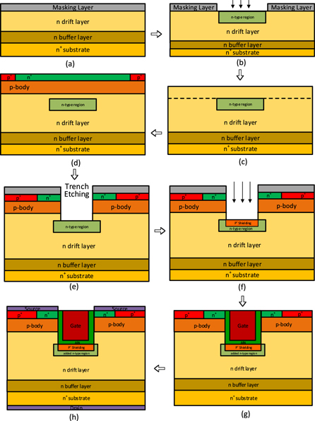
Figure 7. Fabrication feasibility procedure of High-κ TS-UMOSFET.
Download figure:
Standard image High-resolution image3. SEB simulation results and discussion
The SEB simulation results are analysed and discussed in this section. Based on the findings, HK TS-MOSFET was identified to be harder and less sensitive to SEB compared to UMOSFET. The improved performance of HK TS-MOSFET was due to the presence of high-κ dielectric material as the gate oxide, with added n-region covering the P+ shielding region along with an optimised buffer layer. The high-κ dielectric maintains a moderate electric field at the gate oxide, while the P+ shielding region provides additional leak path for hole currents and the buffer layer reduces the impact ionization at the junction of the drift layer and substrate [18, 22].
The SEB's performance of power UMOSFET was extensively investigated using a heavy-ion strike model with variable voltage from drain to source while keeping the gate voltage constant at zero. The position of ion collision is defined by the entrance and exit in the x and y directions, respectively. Therefore, when the power UMOSFET is biased off, the energy ions that strike the structure trigger the parasitic bipolar transistor causing SEB. In order to investigate the SEB trigger mechanism, the most vulnerable heavy ion strike position needs to be ascertained as the device is highly affected by it compared to the other strike positions. The 3 different positions chosen for the assessment are positions (a) x0 = 0μm, (b) x0 = 0.7μm and (C) x0 = 1.25μm (table 3) (figure 8). Based on the observations, position x0 = 0μm was identified as the most sensitive position of SEB for both the conventional and proposed device. Subsequently, the effects of various LETs were simulated under different drain bias voltages as listed in table 4. Since an increase in LET after 0.6pC / μm did not affect the occurrence of SEB, LET = 0.6pC / μm heavy ions were generated at different incidents and transient drain performances were investigated for several drain bias voltages. As a result, the LET value of 0.6pC/μm and ions track position (a) were chosen to investigate the SEB performance in the proposed device.

Figure 8. Simulation of half-cell device structure for heavy ion strikes at different position.
Download figure:
Standard image High-resolution imageTable 3. Sensitive Position Determination for power UMOSFET
| Position | Vds (V) | ||||
|---|---|---|---|---|---|
| 30 | 40 | 50 | 65 | 68 | |
| (a) | N | Y | Y | Y | Y |
| (b) | N | N | Y | Y | Y |
| (c) | N | N | N | Y | Y |
Note.
aY = SEB effect is present, N = SEB effect is absent.Table 4. SEB Simulation Results with Different LET Values for power UMOSFET
| LET (pC/μm) | Vds (V) | |||||||
|---|---|---|---|---|---|---|---|---|
| 30 | 40 | 45 | 50 | 55 | 60 | 65 | 68 | |
| 0.1 | N | N | N | N | N | N | Y | Y |
| 0.3 | N | N | N | N | N | Y | Y | Y |
| 0.4 | N | N | N | N | Y | Y | Y | Y |
| 0.6 | N | Y | Y | Y | Y | Y | Y | Y |
| 0.9 | N | Y | Y | Y | Y | Y | Y | Y |
Note.
aY = SEB is present, N = SEB is absent.In addition, the time variation of the hole-concentration distribution when the SEB of the HK TS-UMOSFET is triggered is depicted in figure 9. The evolution of the hole concentrations inside the structure following an ion's strike time at 5ps, 50ps, 150ps and 1ns was extracted for from a drain voltage of 40 V at a LET = 0.6pC/μm. These variations are helpful in understanding the mechanism of the SEB effect. At 5ps, the holes were distributed in the P+ region, channel and part of the drift region. When the hole concentration of p-body increased to 50ps, parasite BJT was activated. At 150ps, the distribution of the holes in the drift layer was wider and filled up with a device. During this time, many holes are injected into the channel which turns ON the parasite BJT. Even after t = 1 ns, the concentration of the holes kept increasing and the transient current remained high. Hence, when the SEB effect was triggered, the proposed device was exhausted.

Figure 9. Distribution of the hole concentration during the time evaluation of (a) 5ps, (b) 50ps, (c) 150ps and (d) 1ns after an ion's strike at LET = 0.6pC/μm.
Download figure:
Standard image High-resolution imagefigure 10 compares the hole distribution in UMOSFET, TS-UMOSFET and the HK TS-UMOSFET following the ion strike at VDS = 40 V. Based on the observation, the hole concentration at t = 150ps and t = 1 ns for the conventional structure reached a high concentration rate which subsequently caused SEB. To the contrary, the hole concentration decreased to a very low level for the HK TS-UMOSFET due to the high-κ gate oxide material, the shielding region at the bottom of the trench and the presence of buffer layer.

Figure 10. Hole concentrations of (a,b) UMOSFET, (c,d) TS-UMOSFET and (e,f) hardened High-κ TS-UMOSFET at t = 150 ps (left) and t = 1ns (right) after an ion's strike at LET = 0.6pC/μm.
Download figure:
Standard image High-resolution imageChanges in an electric field can also reflect on the impact of single event effects on a devices performance. Figure 11(a) represents a preliminary investigation conducted to assess the influences of high-κ dielectric material on the electric field under VDS = 50 V following an ion strike at t = 150ps. The higher electric field was found to exist at the trench corner and junction of  . The high-κ dielectric material reduces the electric field compared to standard gate oxide. The peak electric field of TS-UMOSFET using SiO2 yielded 3.22 × 10⁵ V/cm, while using high-κ dielectric namely Al2O3, Si3N4 and AlN yielded 1.16 × 10⁵ V/cm, 1.12 × 10⁵ V/cm and 0.8 × 10⁵ V/cm, respectively. In addition, the distribution of the electric field was also noticed during an ion strike at t = 1 ns (figure 11(b)). A similar trend was also observed, where the peak electric field at the junction was estimated at 1.37 × 10⁵ V/cm for AlN compared to 5.78 × 10⁵ V/cm for SiO2. Hence, AlN material was identified as a promising gate oxide to reduce the electric field in the TS-UMOSFET.

Figure 11. Electric field characteristics of the silicon dioxide and high-κ dielectrics as gate oxide in TS-UMOSFET after an ions strike at (a) t = 150 ps (b) t = 1 ns.
Download figure:
Standard image High-resolution imageA comparison of the electric field distribution inside the structure for the standard UMOSFET, TS-UMOSFET and HK TS-UMOSFET is presented in figure 12(a). The peak electric field of the standard UMOSFET was measured at 4.69 × 10⁵ V/cm, while for TS-UMOSFET it was 3.22 × 10⁵ V/cm at t = 150ps. However, the electric field in the drift layer of the hardened TS-UMOSFET was lowered to 0.8 × 10⁵ V/cm, due to the spread-out distribution of the electric fields. The electric field distribution of the standard UMOSFET and hardened TS-UMOSFET at t = 1 ns after an ion strike was depicted in figure 12(b). Based on the observation, high electric field recorded a peak value of 5.78 × 10⁵ V/cm compared to 2.67 × 10⁵ V/cm for standard oxide and 1.37 × 10⁵ V/cm with high-κ oxide.

Figure 12. Electric Field distributions of standard UMOSFET, TS-UMOSFET and hardened HK TS-UMOSFET after an ions strike at (a) t = 150 ps (b) t = 1 ns.
Download figure:
Standard image High-resolution imageIn standard MOSFET, the electric field observed in the simulated structures consistently peaks at the P+ body/ N- drift junction towards the end of the simulation. This observation was possible through the highly localized current which passes along the right side of each structure. For instance, a bulk of the current passes between the inherent parasitic npn transistor (n+ cathode/p- body/ n- drift). Similarly, when a simulation reaches the end, the electric field also peaks at the homo-junction (n- drift/n+ substrate) for UMOSFET, TS-UMOSFET and HK TS-UMOSFET. A strong avalanche rate is formed at a maximum electric field as the ionisation coefficients are exponentially related to the electric field. Thus, the generated currents lead to thermal runaway and burnout. Furthermore, the peak electric field is directly proportional to the impact ionisation coefficient, which is related to the SEB sensitivity [23, 24]. Hence, the reduction of the peak electric field will improve the SEB performance [25]. The ionisation coefficients of the hardened structure are relatively low. The lower electric field results in a less sensitive device towards SEB. Thus, the proposed structure achieved a 76.3% lower electric field compared to the conventional structure.
The changing of drain current as a function of time after a single heavy ion strikes the device for the standard and various high-κ dielectric used in TS-UMOS is demonstrated in figure 13. The response indicated that the transient current increases rapidly to reach a maximum value of less than 100ps. Next, the hole current that was generated at the termination of the simulation was not able to be sustained without parasitic BJT, hence, the current dropped to zero immediately. In addition, standard devices generate higher currents at higher drain voltages, while the hardened structure yield lower currents at the same VDS. Therefore, in short, the drain voltage can significantly affect the triggering of the SEB because higher VDS represents a wider space of charge region resulting in a larger transient current.

Figure 13. Drain current versus time for the silicon dioxide and high-κ dielectrics as gate oxide in TS-UMOSFET after an ion strike.
Download figure:
Standard image High-resolution imageThe drain SEB threshold voltage is considered as one of the main indexes to characterise a devices SEB performance. Table 5 summarises the SEB threshold voltage simulation results of the devices for different biased voltages. In addition, figures 14(a) and (b) represent the drain currents of TS-UMOSFET and HK TS-MOSFET at different biased conditions after an ion strike with a LET of 0.6pC/μm. The SEB occurred at a drain voltage of 53 V for TS-MOSFET, while no SEB was observed at 50 V. As for the proposed structure, the SEB threshold voltage was 67 V, but at 64 V no SEB was recorded. However, at a critical LET value, the proposed structure generated a greater SEB threshold voltage with an improved percentage of 26.41%. Although the proposed structure increased the SEB threshold voltage, the power performance needs to be considered to use as a practical device in the applications.

Figure 14. Analysis of drain current versus time under different drain voltages at ion strike (LET = 0.6pC/μm) (a) Conventional TS-UMOSFET (b) Proposed HK TS-UMOSFET.
Download figure:
Standard image High-resolution image
4. Conclusion
The SEB performance of TS-UMOSFET was assessed for various possible high-κ dielectric gate oxide materials. The 2-D numerical simulation employed in this study predicted a shift in the threshold and breakdown voltage for high-κ dielectrics with fixed layer thickness. Based on the findings, high-κ dielectrics significantly reduced the amount of electric field and drain current during the heavy ion strike compared to conventional SiO2 gate dielectric. The simulation results also indicated that (AlN) is a promising material for SEB hardened TS-UMOSFETs to maintain the improved SEB performance and electric characterisation. Since the SEB threshold voltage for HK TS-UMOSFET was recorded at 67 V compared to 53 V for TS-UMOSFET that were obtained at the same LET value of 0.6pC/μm, the proposed device demonstrated high resistance towards SEB compared to the standard power UMOSFET.
Acknowledgments
This research was funded by Yayasan UTP Fundamental Research(YUTP) under grant number 015LC0-069. The authors would like to thank Universiti Teknologi PETRONAS (UTP), Malaysia for supporting this work.