
Abstract
We investigated the temperature dependence of resistivity in thin crystals of FeSe1−xTex (x = 1.0, 0.95, and 0.9), though bulk crystals with 1.0 ≧ × ≧ 0.9 are known to be non-superconducting. With decreasing thickness of the crystals, the resistivity of x = 0.95 and 0.9 decreases and reaches zero at a low temperature, which indicates a clear superconducting transition. The anomaly of resistivity related to the structural and magnetic transitions completely disappears in 55- to 155-nm-thick crystals of x = 0.9, resulting in metallic behavior in the normal state. Microbeam x-ray diffraction measurements were performed on bulk single crystals and thin crystals of FeSe1−xTex. A significant difference of the lattice constant, c, was observed in FeSe1−xTex, which varied with differing Te content (x), and even in crystals with the same x, which was mainly caused by inhomogeneity of the Se/Te distribution. It has been found that the characteristic temperatures causing the structural and magnetic transition (Tt), the superconducting transition (Tc), and the zero resistivity (Tczero) are closely related to the value of c in thin crystals of FeSe1−xTex.
Export citation and abstract BibTeX RIS

Original content from this work may be used under the terms of the Creative Commons Attribution 4.0 licence. Any further distribution of this work must maintain attribution to the author(s) and the title of the work, journal citation and DOI.
1. Introduction
Iron-based superconductors have been the subject of active research since the discovery of superconductivity at a high superconducting transition temperature (Tc) of 26 K in LaFeAsO1−xFx [1]. The value of Tc increases when LnFeAsO1−xFx contains a rare-earth atom (Ln) with a smaller ionic radius, and it attains a maximum value of 55 K in Sm[O1−xFx]FeAs [2]. These superconductors commonly contain anti-PbO-type FeAs layers as the superconducting layers in the crystal structure. Subsequently, superconductivity at 8 K has been reported in the anti-PbO-type structured FeSe [3], which has the simplest structure of iron-based superconductors and is referred to as a 11-type iron-based superconductor. The Tc value increases up to 37 K when a pressure of 7 GPa is applied to FeSe [4]. Moreover, superconductivity was achieved with a Tc as high as 30–32 K in A1−xFe2−ySe2 (where A = K, Rb, Cs, and Tl), in which an alkali metal atom is intercalated into FeSe layers [5–8]. The metal-intercalated FeSe and FeSe0.5Te0.5 materials that show a superconducting transition up to 46 K were also synthesized by use of the liquid NH3 technique, in which an NH3 molecule or an amine is intercalated with metal atoms [9–12]. Furthermore, a pressure-driven high-Tc superconducting phase was realized in Tl0.6Rb0.4Fe1.67Se2 at 12.4 GPa, and K0.8Fe1.7Se2 at 12.5 GPa, reaching Tc = 48.0–48.7 K [13], and in (NH3)yCs0.4FeSe at 21 GPa, reaching Tc = 49 K [14].
With substitution of Te for Se, the Tc increases up to a maximum value of 14 K at x = 0.6–0.7 in FeSe1−xTex, and the superconductivity disappears at x = 1, i.e., in FeTe [15, 16]. Non-superconducting FeTe exhibits antiferromagnetic ordering below 67 K with a tetragonal-monoclinic structural phase transition. Interestingly, it was reported that FeTe thin films on oxide substrates exhibited superconductivity with a Tc of 13 K, which may be induced by interfacial stress, such as the tensile stress due to a lattice mismatch between FeTe and oxide substrates [17]. Furthermore, it has been reported that single-layer FeSe films show superconductivity at Tc ∼ 85 K, as confirmed by a magnetic susceptibility drop [18], and at Tc > 100 K, as seen from the temperature dependence of in situ four-point probe electrical transport [19]. The opening of a superconducting gap in single-layer FeSe films was observed by angle-resolved photoemission spectroscopy, in which a Tc of 65 ± 5 K was evidenced [20, 21]. Novel physical properties, although never observed in bulk crystals, may even be expected in thin single crystals, since the single-layer FeSe or FeTe thin film exhibits a drastic change in physical properties, as described above. Thus, the 11-type iron-based compound, FeSe1−xTex, would be one of the most suitable candidates for pursuing the novel physical properties of thin crystals because the compound is a layered material, and mechanical micro-exfoliation is available for producing the thin crystals, in the same manner as graphene.
In this paper, we investigated the transport properties in thin crystals of FeSe1−xTex (x = 1.0, 0.95, and 0.9) fabricated by mechanical micro-exfoliation. The temperature dependence of resistivity in thin crystals of x = 0.95 and 0.9 clearly demonstrated remarkable changes, in that the resistivity anomaly related to the structural and magnetic transition is suppressed and/or completely disappears, including the superconducting transition. In contrast, superconductivity was hardly observed for x = 1.0. In order to elucidate the origin of these behaviors, we performed microbeam x-ray diffraction measurements both for the thin crystals and the bulk crystals, which provided significant information about the lattice constant c that corresponds to the direction perpendicular to the FeTe(Se) layers. Through this study, it was found that the temperatures of the anomaly in resistivity and the superconducting transition vary depending on the value of c in thin crystals of FeSe1−xTex.
2. Experimental details
The 35- to 170-nm-thick crystals of FeSe1−xTex (x = 1.0, 0.95, and 0.9) were prepared by mechanical exfoliation of as-grown single crystals with each x by using the scotch-tape. Details of the growth of FeSe1−xTex single crystals are described in [15]. The obtained thin crystal was placed on a 300-nm-thick SiO2/Si substrate. The four-point terminal electrodes were patterned on the single crystal/SiO2/Si substrates by photolithography. Cr and Au were then evaporated at 10−7 Torr for deposition at thicknesses of 5 and 50–100 nm, respectively. After the resist on the substrates was removed, the preparation of samples for resistivity measurement was completed, as shown in figures 1(a)–(c). The thickness of the thin crystals was estimated using atomic force microscope (AFM) system (SII Nano Technology SPA400).

Figure 1. Optical microscope images of four-point terminal devices in FeSe1−xTex, (a) x = 1.0 (#10–1), (b) x = 0.95 (#095–1), and (c) x = 0.9 (#09–2). (d) Atomic force microscope image of x = 1.0 (#10–1) and (e) its profile curve at the line in (d).
Download figure:
Standard image High-resolution imageTemperature-dependent resistivity measurements were performed using a Quantum Design Physical Property Measurement System (PPMS). The resistivity measured in this study is the in-plane resistivity. Microbeam x-ray diffraction measurements were carried out in the BL13XU beamline at SPring-8 [22]. Diffraction patterns from the thin crystals and the bulk crystals were recorded using microbeam x-rays with an energy of 9.998(2) keV (wavelength: 1.2401(2) Å). All such measurements were performed at room temperature. The beam size was 0.4 μm in radius, which is small enough to measure the channel region of thin crystals with electrodes. The 004 diffraction from FeSe1−xTex was detected, together with the 400 diffraction from the substrate Si for x-ray energy calibration. The 004 Bragg peak was fitted by Gaussian function to estimate the c value of FeSe1−xTex.
3. Results and discussion
3.1. Temperature dependence of resistivity in FeSe1−xTex (x = 1.0, 0.95, and 0.9)
Figure 1(a)–(c) show the optical microscope images of typical four-point terminal devices in FeSe1−xTex. The thickness of the thin crystals of FeSe1−xTex (x = 1.0, 0.95, and 0.9) used in the resistivity and microbeam x-ray diffraction measurements was estimated using an AFM as shown in figures 1(d) and (e). The bulk crystals (#10–0, #095–0, and #09–0) refer to small pieces of 30- to 70-μm-thick as-grown single crystals, while details of thin crystals are fully shown in table 1. Figure 2(a)–(c) show the temperature-dependence of the resistivity in the range of 2–300 K for different thicknesses of FeSe1−xTex with x = 1.0, 0.95 and 0.9. Note that the absolute values of resistivity showed no logical order for each concentration. A possible reason for this is that the correction factor for the four-point probe resistivity measurement was not considered in our results. The resistivity value should be precisely evaluated when considering the correction factor value that is related to the size of crystals (length, width, and thickness) and the probe tip spacing with the four-point probe technique [23]. Although the bulk and thin crystals had various shapes and sizes in this study, we evaluated the resistivity as an ideal case without including the correction factor. Therefore, the absolute resistivity values might slightly vary, resulting in no logical order for each concentration. The bulk (#10–0) and thin crystals (#10–1 and #10–2) of FeTe (x = 1.0) exhibit an anomaly in resistivity related to the structural and magnetic transition at around 50–60 K, and no superconducting transition (see figures 2(a) and (d)). Here we define Tt as the temperature of an anomaly in resistivity related to the structural and magnetic transition. The Tt of thin crystals decreases in comparison with that of bulk crystal, and the resistivity anomaly is broadened. However, the anomaly does not completely disappear even at a thickness of 70 nm, and no superconducting transition is observed. The study of 60- to 150-nm-thick FeTe thin films on oxide substrates, which was reported by Han et al, showed that the resistivity anomaly due to the first-order magnetic and structural transition was broadened, and superconductivity with an onset superconducting transition temperature Tconset of 13 K suddenly emerged [17]. This result suggested that out-of-plane contraction (uniaxial pressure) was important to induce superconductivity in the FeTe system, which is accompanied by in-plane extension of FeTe film on oxide substrates. However, the application of hydrostatic pressures up to 19 GPa could not induce superconductivity in polycrystalline FeTe0.92 [24]. Therefore, the application of greater pressure along the c-axis (out-of-plane) may be indispensable for inducing superconductivity in FeTe thin crystals.
Table 1. Summary of the parameters, thickness, lattice constant c, Tt, Tc, Tczero, and ΔTc of FeSe1−xTex (x = 1.0, 0.95, and 0.9) thin crystal samples. Thickness is measured using AFM and is estimated by the width of the microbeam x-ray diffraction peak in terms of the Scherrer equation. Lattice constant c is determined from diffraction patterns. Tt, Tc, Tczero, and ΔTc are determined from resistivity data. Resistivity measurement was not performed on #10–3 and #095–2.
| x = 1.0 Sample ID | Thickness by AFM (nm) | Thickness by XRD (nm) | c (Å) | Tt (K) | Tc (K) | Tczero (K) | ΔTc (K) |
|---|---|---|---|---|---|---|---|
| #10–0 | ∼30 × 103 | — | 6.274(5) | 59.6 | — | — | — |
| #10–1 | 170 | 120(26) | 6.268(1) | 50.5 | — | — | — |
| #10–2 | 70 | 45(5) | 6.277(3) | 53.4 | — | — | — |
| #10–3 | 35 | 84(4) | 6.2668(2) | (Not measured) | |||
| x = 0.95 Sample ID | Thickness by AFM (nm) | Thickness by XRD (nm) | c (Å) | Tt (K) | Tc (K) | Tczero (K) | ΔTc (K) |
| #095–0 | ∼50 × 103 | — | 6.260(2) | 48.9 | 7.0 | — | — |
| #095–1 | 170 | 112(8) | 6.2637(9) | 42.3 | 10.4 | — | — |
| #095–2 | 120 | 104(5) | 6.2640(5) | (Not measured) | |||
| #095–3 | 90 | 57(4) | 6.2616(9) | 39.1 | 11.5 | 3.0 | 8.5 |
| x = 0.9 Sample ID | Thickness by AFM (nm) | Thickness by XRD (nm) | c (Å) | Tt (K) | Tc (K) | Tczero (K) | ΔTc (K) |
| #09–0 | ∼70 × 103 | — | 6.25(1) | 33.3 | 12.7 | — | — |
| #09–1 | 155 | 140(1) | 6.2422(6) | — | 13.2 | 10.4 | 2.8 |
| #09–2 | 100 | 108(9) | 6.2399(9) | — | 13.3 | 11.7 | 1.6 |
| #09–3 | 55 | 39(3) | 6.236(2) | — | 12.9 | 11.1 | 1.8 |
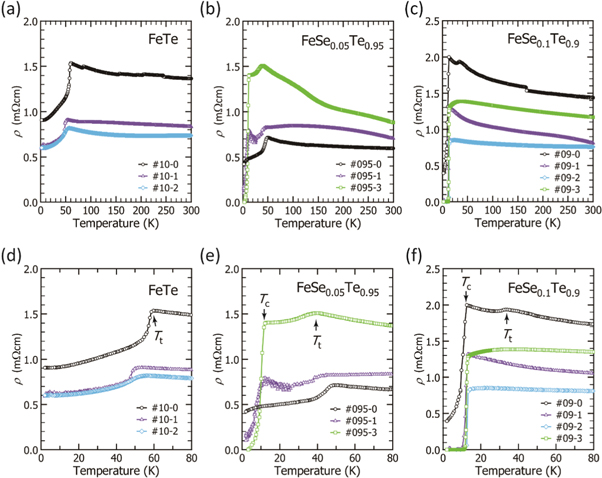
Figure 2. Temperature dependence of resistivity for thin single crystals of (a) FeTe, (b) FeSe0.05Te0.95, and (c) FeSe0.1Te0.9. (d)-(f) Low-temperature resistivity of (a)–(c).
Download figure:
Standard image High-resolution imageAs shown in figures 2(b) and (c), the resistivity anomaly is also observed in the temperature dependence of resistivity for bulk single crystals of FeSe1−xTex with x = 0.95 (#095–0) and 0.9 (#09–0), in which the superconducting transition is not clearly found for x = 0.95 (#095–0). However, we found the superconducting transition in their mechanically exfoliated thin crystals. A clear drop in resistivity is observed at Tc of 10.4 K and 11.5 K in 170- and 90-nm-thick FeSe0.05Te0.95 (#095–1 and #095–3), respectively, although the resistivity anomaly is still observed (see figures 2(b) and (e)). Finally, the resistivity of the 90-nm-thick FeSe0.05Te0.95 (#095-3) reaches zero at a Tczero of 3.0 K, but the superconducting transition temperature width ΔTc (= Tc–Tczero) is large (ΔTc = 8.5 K), as seen in figure 2(e). Here we define Tc as the intersection of the tangent at the inflection point of the resistive transition and a straight-line fit of the normal state just above the transition, and Tczero as the temperature reaching zero resistivity. In thin crystals of FeSe0.1Te0.9, as shown in figures 2(c) and (f), the anomaly completely disappears and a sharp superconducting transition is observed at a Tc of 13.2 K (#09–1, 155 nm), 13.3 K (#09–2, 100 nm), and 12.9 K (#09–3, 55 nm). With decreasing thickness, the transition width becomes smaller, with ΔTc = 2.8 K to 1.6 K, as seen from figure 2(f). Interestingly, the temperature dependence of resistivity in the normal state of FeSe0.1Te0.9 shows a gradual change from semiconducting to metallic behavior with decreasing thickness (figure 2(f)). Such behavior has also been observed in the substitution of Se for Te [15] and in the enhancement of annealing temperature of single crystal Fe1+ySe0.4Te0.6 [25]. The inhomogeneity of Se/Te distribution and the presence of 'excess Fe', which are strongly related to the physical properties of FeSe1−xTex, have been discussed in references [25–27] as one of the origins of such semiconductor-metal transition; 'excess Fe' refers to Fe atoms not forming part of the structure of FeSe1−xTex. To summarize the transition temperatures for FeSe1−xTex crystals with various thickness, the Tt, Tc, Tczero, and ΔTc are plotted as a function of thickness as shown in figure 3(a) (x = 1.0), (b) (x = 0.95), and (c) (x = 0.9). The superconductivity tends to be clearly observed in the thinner crystals in x = 0.95 and 0.9 as discussed above. One possibility is that heating in the lithography process makes thin crystals homogeneous and improves superconductivity. Our photolithography method includes heating at 110 oC for 6.5 min and at 180 oC for 3 min in air for the prebaking of photoresist. These temperatures and times are much lower and shorter than those in previous reports, e.g., 200 °C–300 oC for 2 h in air [25] and 400 oC for more than 10 days in vacuum [28], for changing the transport property. For ∼100-nm-thick crystals, however, such a process may not only reduce the amount of excess Fe, but also effectively enhance a homogeneity of Se/Te distribution.

Figure 3. Tt, Tc, Tczero, and ΔTc of FeSe1−xTex ((a) x = 1.0, (b) 0.95, and (c) 0.9) bulk and thin crystals as a function of thickness.
Download figure:
Standard image High-resolution image3.2. Microbeam x-ray diffraction measurement in FeSe1−xTex (x = 1.0, 0.95, and 0.9)
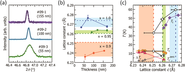
To explore the origin of the difference in the temperature dependence of resistivity between bulk and thin crystals of FeSe1−xTex, we investigated the variation in the c value corresponding to the FeSe1−xTex interlayer distance. The value of c was determined from the 004 Bragg peak of FeSe1−xTex by microbeam x-ray diffraction measurements. The diffraction patterns were measured at several different positions in the same crystal. The average c values with the estimated standard deviations are listed in table 1. Figure 4(a) shows the 004 Bragg peaks of the thin crystals of FeSe0.1Te0.9. The width of the diffraction peak becomes broader with decreasing thickness. The broadening of a diffraction peak is related to the size of the sub-micrometer particles (crystallites) in a solid. The crystalline size, i.e., the average thickness along the c-axis, of thin crystals is roughly estimated in terms of the Scherrer equation, with the shape factor K = 0.94, to be 140(1) nm (#09–1), 108(9) nm (#09–2), and 39(3) nm (#09–3). These values correlate with the thickness determined by AFM and an approximate trend of thickness of thin crystals can be obtained, as listed in table 1.
Figure 4. (a) Bragg peaks from the (004) plane of FeSe0.1Te0.9 thin crystals. The black lines are fits to Gaussian function. (b) Thickness dependence of lattice constant c in thin crystals of FeSe1−xTex (x = 1.0, 0.95, and 0.9). Error bars represent the results of diffraction patterns at several positions. (c) Tt (◆), Tc (●), Tczero (▲), and ΔTc (✦) of FeSe1−xTex (x = 1.0, 0.95, and 0.9) bulk (white markers) and thin (color markers) crystals as a function of lattice constant c. Dashed lines and color bars (blue: x = 1.0, green: x = 0.95, and orange: x = 0.9) in (b) and (c) correspond to the average c values of bulk crystals and the variation width of the c value for all crystals, respectively.
Download figure:
Standard image High-resolution image
The c value of bulk crystal decreases with increasing Se quantity (decreasing x), which is consistent with previous studies [29–31]. The standard deviations of the c values for bulk crystals are larger than that of thin crystals, reflecting the large inhomogeneity of the presence of excess Fe and Se/Te distribution by Se doping. On the other hand, the variation in the c value of thin crystals with different thicknesses for each x does not show a unified trend, as seen in figure 4(b). A tendency for swelling along the c-axis with thinning of the crystal was reported in nano-thick crystals (thickness, 14–31 nm) of 1T-TaS2 [32], in which the charge-density-wave (CDW) transitions were systematically controlled by changing thickness. In the case of FeSe1−xTex, however, the value of c does not simply depend on the thickness of thin crystals, probably because of various factors such as inhomogeneity of Se/Te distribution and inhomogeneous distribution of excess Fe. This may cause the different behavior of temperature-dependent resistivity of thin crystals. Indeed, inhomogeneous superconductivity was observed in the temperature dependence of resistivity in the 15- to 100-nm-thick crystals of FeSe0.35Te0.65 [26] and in the 12- to 90-nm-thick crystals of FeSe0.5Te0.5 [27]. These results suggested that the different superconducting behavior in these thin crystals with different thickness might be related to the inhomogeneous distribution of excess Fe [26, 27] and/or the inhomogeneity of Se/Te distribution [27], and the temperature dependence of resistivity in the thin crystal that was taken from the low concentration region of excess Fe in the bulk crystal showed a sharp superconducting transition and homogeneous superconductivity [26]. A narrowing of superconducting transition width ΔTc was observed in the case of thinner single crystals of x = 0.95 and 0.9, as seen in table 1, which can be explained by a scenario proposed in reference [26] as mentioned above, but there is no direct evidence to determine whether the thin crystal contains a low concentration of excess Fe or not. The c value may be one of the parameters to confirm a variation in the amount of excess Fe and the homogeneity of Se/Te in FeSe1−xTex.
3.3. Correlation between the lattice constant c and transport properties
In order to clearly indicate a relationship between the superconductivity and the c values of thin crystals, the characteristic temperatures, Tt, Tc, Tczero, and ΔTc are plotted as a function of c in figure 4(c). The color bars (blue, green, and orange) indicate the variation width of the c values for x = 1.0, 0.95, and 0.9, respectively. With decreasing c, Tt becomes lower, and then a superconducting transition (plot of Tc) appears. Furthermore, zero resistivity (plot of Tczero) is observed and the Tczero increases with the narrowing of ΔTc. In the study of Fe1+δTe reported by T. Machida et al, the different Tt was caused by an inhomogeneous distribution of excess Fe. However, the Tt did not show any monotonic change with a decrease in the amount of excess Fe, while the c value monotonically increased with a decreasing amount of excess Fe [33]. Therefore we can't conclude that the amount of excess Fe decreases with decreasing thickness for x = 1.0, but the lower Tt was realized in FeTe thin crystals with a smaller c value. Furthermore, in FeySe0.5Te0.5 (y = 0.95–1.10), more metallic behavior in the normal state, a clearer superconducting transition, and an increase in the c value were observed with decreasing amount of excess Fe [34]. This trend is not consistent with our result showing more metallic behavior and clearer superconducting transition with a decrease in the c value.
On the other hand, from the viewpoint of the Se/Te distribution, the c value tends to decrease monotonically with increasing Se content. The increase in the Se content is more suitable for stabilizing the metallic and superconducting states, as suggested from the comparison with non-superconducting FeTe. In our study, the metallic and superconducting states are stabilized as the c value decreases, indicating that the stabilization cannot be associated with a decrease in the amount of excess Fe, which results in an increase in c. Thus, a change of the amount of excess Fe that influences the c value may not occur in exfoliated thin crystals of FeSe1−xTex. Therefore, the result indicates that the inhomogeneity of the Se/Te distribution of bulk crystals may sensitively affect the metallic and superconducting states in thin crystals of FeSe1−xTex with low Se content (high Te content; x  0.9), and exfoliation and/or heating in the photolithography process make thinner crystals more homogeneous Se/Te distribution. The phase diagram was well drawn by plotting the characteristic temperatures against the c value of the thin crystals with different Te content (x) and thickness. Yue et al reported that fluctuation in the Se/Te distribution and/or the presence of a trace amount of excess Fe led to nanoscale phase separation [27]. The superconductivity was suppressed below a critical thickness of ∼12 nm in FeSe0.5Te0.5 due to the lack of a continuous superconducting path, while the superconducting islands were well connected and formed robust superconducting paths in thick crystals (thickness >40 nm). In our study, the crystal thickness of 35–170 nm is enough to form three-dimensional (3D) superconducting paths, and a low dimensional effect (size effect) such as the two-dimensional (2D) quantum confinement effect may be eliminated.
4. Conclusions
We investigated the temperature dependence of resistivity in thin crystals of FeSe1−xTex (x = 1.0, 0.95, and 0.9) that are non-superconducting in bulk crystals. With decreasing thickness of the crystals, the temperature dependence of the resistivity of x = 0.95 and 0.9 clearly shows a superconducting transition, providing zero resistivity with a narrow ΔTc. A significant difference of the lattice constant c was observed in FeSe1−xTex with different Te content (x), and even in that with the same x, which is presumably caused by an inhomogeneity of the Se/Te distribution. The characteristic temperatures, Tt, Tc, and Tczero, clearly depend on the c values. Our result indicates that local structural distortion occurs owing to inhomogeneity of the Se/Te distribution and affects the transport property of the FeSe1−xTex thin crystals.
Acknowledgments
This study was partly supported by Grants-in-Aid for Scientific Research (23684028, 22244045, 24654105, 18K04940, 19H02676) from MEXT, by the Program to Disseminate the Tenure Tracking System of the Japan Science and Technology Agency (JST), and by the Program for Advancing Strategic International Networks to Accelerate the Circulation of Talented Researchers from JSPS (R2705). The synchrotron radiation experiments were performed at BL13XU of SPring-8 with the approval of the Japan Synchrotron Radiation Research Institute (JASRI) (Proposal No. 2015B1206).