

Abstract
Linear nonsaturating magnetoresistance (LMR) represents a class of anomalous resistivity response to external magnetic field that has been observed in a variety of materials including but not limited to topological semi-metals, high-Tc superconductors and materials with charge density wave (CDW)/spin density wave orders. Here we report the observation of LMR in layered kagome superconductor and CDW material CsV3Sb5 thin flakes, as well as the dimensional crossover and temperature (T) crossover of such LMR. Specifically, in ultrathin CsV3Sb5 crystals, the magnetoresistance (MR) exhibits a crossover from LMR at low T to quadratic B dependence above the CDW transition temperature; the MR also exhibits a crossover from LMR to sublinear MR for sample thickness at around ∼20 nm at low T. We discuss several possible origins of the LMR and attribute the effect to two-dimensional CDW fluctuations. Our results may provide a new perspective for understanding the interactions between competing orders in kagome superconductors.
Export citation and abstract BibTeX RIS
1. Introduction
Linear nonsaturating magnetoresistance (LMR) is an unconventional transport phenomenon that the longitudinal electrical resistivity of the material increases linearly with external magnetic field (B). LMR is scientifically interesting [1–6] and potentially useful in applications such as magnetic sensors [7–9], attracting considerable attention from the materials science community. LMR materials include narrow band-gap disordered semiconductors [1, 7, 8, 10–13], topological semi-metals with linear dispersion relation [2, 4, 14, 15], various materials with charge/spin density wave (CDW/SDW) orders [16–18], and high-Tc superconductors [6]. However, an important type of topological materials, e.g. layered materials with kagome lattice, has not been found to exhibit LMR before.
Kagome metals/insulators have a distinctive band structure, simultaneously possessing flat bands, van Hove singularities and topological surface states, together with the potential to form unique spin/charge orders due to their unique lattice geometry [19, 20]. Thus, kagome materials provide an ideal arena for studying the interplay among electron–electron correlations, topological nontrivial states and lattice symmetry. Recently, a new family of kagome metal AV3Sb5 (A = K, Rb, Cs) has attracted great interest with intertwined exotic orders including unconventional CDW, superconductivity, topological nontrivial states and the possibility of additional hidden orders [20–23]. The unconventional CDW order is manifested in magnetic susceptibility, resistivity and specific heat in the temperature range of 70–100 K [20, 21, 24]. It can also be directly detected by optical spectroscopy [25–27], scanning tunneling microscopy [22, 28, 29] as well as angle-resolved photoemission spectroscopy (ARPES) [30–32]. According to measurements of magnetization, resistivity, and heat capacity, CsV3Sb5 and KV3Sb5 show an onset of superconductivity at 2.5 and 0.93 K respectively [20, 24]. For RbV3Sb5, the onset temperature of superconducting transition in resistance is about 0.92 K and zero resistance temperature sets in about 0.75 K [33]. Unconventional CDW and superconductivity in AV3Sb5 are shown to coexist and compete with each others [34–39], and they are both highly tunable by external pressure [36, 38, 40] and chemical doping [41–43]. To date, the overwhelming majority of the research effort is on bulk AV3Sb5 crystals, where LMR is not observed. Here, we report the discovery of LMR in CsV3Sb5 (CVS) thin flakes (<20 nm) at low temperatures (<30 K) as well as the existence of dimensional crossover and temperature crossover of such LMR.
2. Result and discussion
CVS has an A-A stacked hexagonal lattice structure at room temperature (unit cell of CVS shown in the lower left panel of figure 1(b)). The CVS crystal consists of alternately stacked alkali-metal Cs layers and V–Sb layers along the c axis. Figure 1(b) shows the schematic top view of the crystal structure showing the V and Sb atoms. The V atoms form a two-dimensional (2D) kagome framework with in-plane and out-of-plane covalent bonds to Sb atoms; the V–Sb layers are then intercalated by Cs layers with trigonal symmetry. The relatively weak interactions between the V–Sb layers and the Cs layers make CVS easily cleavable. Thin flakes of CVS single crystals are fabricated into Hall bar devices as shown in figure 1(a). Note that all the device fabrication processes were carried out in an argon glove box or in vacuum, short exposure to air is made only when the device is protected by 160 nm of polymethyl methacrylate (PMMA) layer to prevent sample degradation.

Figure 1. Crystal structure of CsV3Sb5 and resistivity curve. (a) Optical micrograph of a thin CsV3Sb5 flake device. (b) Crystal structure of CsV3Sb5. Blue, red and yellow balls represent cesium, vanadium and antimony atoms respectively. Atomic layers composed of vanadium and antimony atoms are intercalated by cesium atoms, and vanadium atoms forms the kagome network. (d) Temperature dependence of longitudinal resistivity and differential longitudinal resistivity. The clear kink observed at 87.8 K corresponds to the temperature of CDW transition.
Download figure:
Standard image High-resolution imageThe unconventional CDW in CVS results in clear electrical signal in the longitudinal resistivity ρxx . Figure 1(c) shows the T dependence of ρxx as well as dρxx /dT of a CVS thin flake device (sample #3, 12 nm thick). With decreasing temperature, ρxx decreases monotonically with a kink at around 90 K, corresponding to the CDW transition temperature TCDW. The CDW transition is more visible in the dρxx /dT vs. T curve, where a discontinuity appears in the curve at TCDW, which is consistent with previous reports [29]. We extract the precise TCDW ∼ 87.8 K from the dρxx /dT vs. T curve.
Figure 2(a) shows the longitudinal magnetoresistance (MR) of sample #3 (12 nm thick) under perpendicular magnetic field and in the temperature range of 2–120 K. The most striking feature in the MR is its nonsaturating linearity with respect to B at low T. With increasing T, the MR vs. B curves gradually deviate from a linear form to a quadratic form. To quantify such evolution of MR, the MR curves at different T are fitted to a polynomial: MR= α+ β× Bn , where α, β and n are fitting parameters. As shown in figure 2(b), the polynomial fits to the MR curves very well for all the temperatures explored experimentally. The exponent n has a monotonic dependence on T, which is plotted in figure 2(c). It can be seen that at and above TCDW, n ∼ 2, which means that the MR above the CDW transition temperature are of conventional quadratic dependence on B. Below TCDW, n reduces dramatically as T decreases, indicating that the reduction of n is closely related to the onset of the CDW phase transition. When T is below 30 K, n ∼ 1 and remains unchanged, showing that MR vs. B is highly linear and nonsaturating up to 14 T.
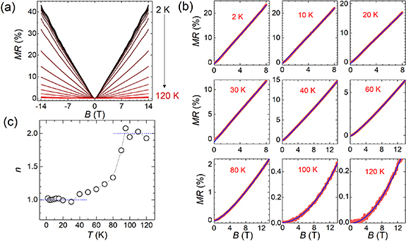
Figure 2. Magnetoresistance of sample #3. (a) Magnetoresistance (MR), defined as (ρxx (B) − ρxx (0))/ρxx (0), as a function of magnetic field at various temperatures. The magnetic field is parallel to the c-axis direction. (b) MR curves at several representative temperatures fitted to α+ β× Bn , where α, β and n are fitting parameters. The red curves are experiment data and the blue curves are the fitting curves. Only MR data from 0 T to 8 T are fitted to avoid complications from SdH oscillations. (c) The temperature dependence of power exponent n.
Download figure:
Standard image High-resolution imageTo further study this intriguing LMR, we measured the thickness-dependent MR of CVS single crystals. Figure 3(a) plots the MR curves for CVS with different thickness at 10 K. In contrast to the relatively thin samples, the MR of thicker crystals becomes sublinear with B. The same polynomial MR= α+ β× Bn is fitted to the MR curves, and the fitting parameter n has an abrupt change from 1 to 0.7 for sample thickness larger than 20 nm (figure 3(b)). Such a thickness-dependent behavior is consistent with a dimensional crossover in the CDW transition in CVS crystals. Indeed, it has been previously reported that VSe2, another layered CDW material, has a crossover in the Fermi surface topology from three-dimensional (3D) to 2D at around sample thickness of 20 nm [44]. It is also reported that bulk CVS has 3D CDW [45–47], while a dimensional crossover of such CDW order from 3D to 2D has been reported via transport measurement without magnetic field [48]. The above evidence suggests that the unusual LMR discovered in CVS thin flakes is likely connected to the 2D nature of the CDW order.

Figure 3. (a) Magnetoresistance of CsV3Sb5 thin flakes with various thickness at 10 K. Samples #1–#3 are thinner than samples #4–#6; (b) fitting parameter n versus sample thickness. As sample thickness reduces, the fitting parameter n changes from 0.7 to 1, exhibiting a 3D to 2D crossover around 30 nm.
Download figure:
Standard image High-resolution imageNow we turn to the discussion on the possible origin of the LMR. Conventionally, magnetic field changes the electron trajectory and reduces effective electron mean path, giving rise to a positive MR which scales quadratically with B [49]. However, MR could deviate from the quadratic law due to quantum effects, unusual topological band structures and disorders [8, 10, 50]. In particular, LMR has been observed in other materials, such as semiconductors with narrow band gap, unconventional superconductors, topological and CDW/SDW materials [1, 6, 15, 51–53]. Several mechanisms have been proposed to explain LMR. These mechanisms are summarized in the followings and are compared with our experimental findings: (a) the Parish–Littlewood model [8]. This model considers the classical effects of macroscopic disorders and strong inhomogeneity, which lead to the mixing of longitudinal resistance and transverse resistance. With an additional requirement of linear Hall effect, LMR would appear. However, CVS does not have a linear Hall effect both as thin flakes (see figure 4(a)) and as bulk crystals below TCDW [54]. In addition, LMR from the Parish–Littlewood model has no obvious temperature dependence and can emerge at high temperature, which is not the case for CVS. Therefore, the Pairth–Littlewood model could not explain our experimental findings. (b) The Abrikosov model [10]. This model considers a gapless semiconductor with a linear dispersion relation and has only one Landau band participating in transport. Although experiments and theoretical calculations have confirmed that bulk CVS has a nontrivial topological band structures with a linear energy spectrum [20, 55], we have not observed strong evidence of nontrivial topological band structures in ultrathin samples from the analysis of SdH oscillation (see supplementary figure S2(c)). On the other hand, LMR in thin CVS sets in at ∼0.85 T and goes on beyond 8 T. Considering that two main frequencies of SdH oscillations are found (F1 = 31 T and F2 = 64 T, see supplementary figure S2(a)), it is impossible for only one Landau level to participate in the transport in the magnetic field from 0.85 T to 8 T. Hence Abrikosov's model cannot explain our results. (c) The 'hot spots' model [56]. This model considers particular areas or points on the Fermi surface (called 'hot spots') that scatter charge carriers more than other areas. Under nonzero magnetic field, hot spots provide a scattering rate 1/τhs which is linearly dependent on B, which lead to LMR. The linear B dependence of 1/τhs can be understood by a simple picture that in the reciprocal space, the frequency of electrons passing through these hot spots (∼1/τhs) is proportional to the cyclotron frequency ωc, where ωc increases linearly with B. Thus, ρxx ∼ 1/τhs ∼ ωc ∼ B, and the 'hot spots' model may capture the physics of LMR in CVS.
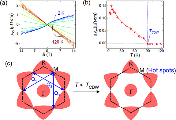
Figure 4. Hall resistivity and hot spot model. (a) The magnetic field dependence of Hall resistivity ρxy at various temperatures. (b) The deviation ρxy from linearity Δρxy as a function of temperature at 2 T. The Δρxy is extracted from ρxy by subtracting a linear background obtained from the ρxy vs. B curves above 5 T. The Hall resistivity with the magnetic field deviates from the linear dependence at and below TCDW. (c) Schematic of Fermi surfaces of CVS in the hexagonal Brillouin zone. Owning to CDW, the Fermi surface is nested by the CDW vectors Q1/2/3 and opens a gap at the M points, making the M points hot spots for carrier scattering.
Download figure:
Standard image High-resolution image
Next, we look into mechanisms to create such hot spots in CVS. First, Young et al proposed that the Fermi surface close to Brillouin zone boundary can be regarded as hot spots because of intense Umklapp phonon scattering [56]. However, Umklapp scattering strongly depends on temperature, while LMR in thin CVS remains invariant to temperature for T< 30 K. Second, hot spots could be attributed to magnetic breakdown [57], which is inconsistent with the fact that LMR in CVS happens at very small magnetic field of 0.8 T and remains nonsaturating up to 14 T. Third, Fermi surface with sharp corners [18] has been proposed to be the source of hot spots. Current ARPES experiment in CVS did show the possibility of Fermi surface with sharp corners, but the resolution is limited. Furthermore, the ARPES experiments are done with bulk CVS crystals that do not show LMR.
With the above discussions, we have narrowed down the possible mechanism to CDW fluctuations [16] that could simultaneously in line with the experimental observation of temperature crossover and dimension crossover in CVS thin flakes. Specifically, (a) the exponent n in MR= α+ β× Bn has a sharp reduction starting at T = TCDW, and (b) LMR appears only in relatively thin films (a dimensional crossover appear at crystal thickness of about 20 nm). The first point shows that LMR in CVS is associated with the onset of CDW. Indeed, recent researches show that the CDW in CVS is driven by the scattering of electrons between neighboring M points [30]. In our experiment, the Fermi surface reconstruction induced by CDW is supported by a deviation from linearity of Hall resistivity Δρxy , such that Δρxy increases rapidly below TCDW (see figure 4(b)). Fermi surface reconstruction actually leads to a complex multiband and consequently gives rise to nonlinear B dependent ρxy , which could be a joint effect of classical multiband and nontrivial Berry phase. Here, Δρxy (B) is extracted from ρxy (B) by subtracting a linear background obtained from the ρxy (B) curves above 5 T, and figure 4(b) plots Δρxy (B = 2 T) vs. temperature. Secondly, since reduced dimension is known to increase fluctuations, destroying lattice order [58], magnetic order [59] and suppressing CDW [60], LMR in CVS thin flakes could stem from 2D CDW fluctuations. Inspired by the hot spots model, we propose that 2D CDW fluctuation could turn the M points to be hot spots for quasi-particle scattering (see figure 4(c)) and lead to LMR in CVS. Since the LMR observed in CVS thin flakes is closely related to the formation of CDW as well as the fluctuation of it at reduced dimension, we expect the temperature and thickness dependent MR of other CVS variants to be significantly modified by the nature of their respective CDW correlations.
In thin flakes CVS at finite temperature, electron scattering is likely dominated by 2D CDW fluctuations, impurities and phonons. The total scattering rate, , is a sum of the contribution from
  (from 2D CDW fluctuations),
  (from impurities) and
  (from phonons). Thus
  , where m is the electron effective mass,
  is the carrier density and e is the elemental charge. Above TCDW, since there is no CDW order,
  ∼B2, leading to the conventional quadratic MR. Because 2D CDW fluctuations appear below TCDW, according to the hot spots model,
  linearly depends on magnetic field, i.e.
  According to Matthiessen's rule for incoherent scatterers, MR below TCDW will be proportional to a sum of the first and second power of the magnetic field (thus the exponent n in MR= α+ β× Bn
has values between 1 and 2). As temperature is considerably lower than TCDW (i.e. T < 30 K) and for strong enough magnetic field,
According to Matthiessen's rule for incoherent scatterers, MR below TCDW will be proportional to a sum of the first and second power of the magnetic field (thus the exponent n in MR= α+ β× Bn
has values between 1 and 2). As temperature is considerably lower than TCDW (i.e. T < 30 K) and for strong enough magnetic field,  and
and  . Therefore, MR becomes linear with magnetic field. This phenomenological theoretical model can explain our results well, and a similar model has been reported to explain LMR in the CDW materials TbTe3 and HoTe3 [16].
Furthermore, superconductivity and LMR coexists in a number of unconventional superconductors, where LMR is considered to be related to specific pairing mechanisms of the superconductor [6, 51]. For example, LMR in cuprate superconductors may be associated with quantum criticality [6], and LMR in ultrathin superconducting FeSe films is considered to arise from spin fluctuation [51]. Our study of the relation of LMR and CDW in kagome superconductor CVS thus provides a new example the competition and intricate relations of quantum orders in materials.
3. Conclusion
In summary, we systematically studied the MR and Hall effect of the topological kagome metal CsV3Sb5, and discovered an unusual LMR with both temperature crossover and dimensional crossover effect. In particular, LMR develops for crystals thinner than 20 nm and below 30 K. For T > TCDW, MR is quadratic in B, and for crystal thickness larger than 30 nm, LMR is not observed from 2 K to 300 K. The temperature-dependent crossover in LMR is accompanied by the appearance of a Hall anomaly, strongly suggesting that both effects arise from Fermi surface reconstruction caused by the CDW order. The dimensional crossover shows that 2D CDW fluctuation is the most likely cause of this unusual linear MR.
4. Experimental section
Single crystal CVS is prepared via the self-flux method [29]. Thin flakes of CVS were exfoliated by Al2O3-assisted exfoliation method [61] onto highly doped silicon wafer with 285 nm SiO2. Then, the electrodes with Hall bar geometry as shown in figure 1(a) were prepared by a standard microfabrication process. Electrodes composed by a bilayer of Ti/Au (5 nm/100 nm) were deposited onto the flakes using e-beam evaporation in high vacuum (10−7 mbar).
Transport measurements are performed at temperatures between 0.5 K and 300 K with magnetic fields up to 14 T in an Oxford Teslatron cryostat and in a Quantum Design PPMS with a 3He insert. Lock-in amplifiers are used to measure longitudinal resistivity (ρxx ) and Hall resistivity (ρxy ) at a frequency of 77.77 Hz. Magnetic field is applied parallel to the c-axis direction. The thickness of various samples is measured by atomic force microscopy.
Acknowledgments
This project has been supported by the National Basic Research Program of China (Grant Nos. 2019YFA0308402 and 2018YFA0305604), the National Natural Science Foundation of China (NSFC Grant Nos. 11934001, 11774010, and 11921005), Beijing Municipal Natural Science Foundation (Grant No. JQ20002), the National Natural Science Foundation of China (Grant No. 92065109), National Key R&D Program of China (Grant No. 2020YFA0308800), and Beijing Natural Science Foundation (Grants Nos. Z210006 and Z190006). Z W thanks the Analysis & Testing Center at BIT for assistance in facility support.
Data availability statement
The data that support the findings of this study are available upon reasonable request from the authors.
Author contributions
J-H C and X W conceived idea and designed the project. Z W grew the single crystals. X W and C T performed the fabrication of devices and the low-temperature measurements with the help of Y F, J C and Y S J-H C and X W wrote the manuscript. All authors discussed the results and commented on the paper.
Supplementary data (0.4 MB PDF)