
Abstract
While the basal plane of graphene is inert, defects in it are centers of chemical activity. An attractive application of such defects is towards controlled functionalization of graphene with foreign molecules. However, the interaction of the defects with reactive environment, such as ambient, decreases the efficiency of functionalization and makes it poorly controlled.
Here, we report a novel approach to generate, monitor with time resolution, and functionalize the defects in situ without ever exposing them to the ambient. The defects are generated by an energetic argon plasma and their properties are monitored using in situ Raman spectroscopy. We find that these defects are functional, very reactive, and strongly change their density from ≈1 × 1013 cm−2 to ≈5 × 1011 cm−2 upon exposure to air. We perform the proof of principle in situ functionalization by generating defects using the argon plasma and functionalizing them in situ using ammonia functional. The functionalization induces the n-doping with a carrier density up to 5 × 1012 cm−2 in graphene and remains stable in ambient conditions.
Export citation and abstract BibTeX RIS

Content from this work may be used under the terms of the Creative Commons Attribution 4.0 licence. Any further distribution of this work must maintain attribution to the author(s) and the title of the work, journal citation and DOI.
1. Introduction
While the properties of pristine graphene are now largely understood, we are only beginning to understand the potential of controllably functionalized graphene. During the last decade, multiple approaches have been developed to attach foreign molecules such as hydrogen, oxygen, fluorine, or organic compounds to the basal plane of graphene [1–6]. Controlled functionalization has been used to open the band gap [7, [8]], adjust the doping levels [9], induce defect states producing photoluminescence [8, 10, 11], or perhaps even to induce magnetism in grapheme [12]. Moreover, graphene controllably functionalized with biomolecules is in demand for applications in filtration, biotechnology, and biosensorics [13, 14].
In general, there are covalent and non-covalent functionalization approaches [2, 15, 16]. In non-covalent functionalization, a target molecule is deposited onto graphene predominantly through interactions like van der Waals forces or π-π stacking [17]. As these interactions are relatively weak, molecules tend to cluster [18] or may be removed during processing of functionalized material [19]. In the covalent approach, a covalent bond forms between graphene and a target molecule. As the basal plane of graphene is highly inert, this functionalization approach requires reactive compounds, e.g. free radicals [2, 3, 19, 20]. At the same time, defects in graphene are the centers of chemical activity [21]. Therefore, many functionalization strategies use these defects to graft desired functionalities [22–28].
One of the most simple, cheap, and scalable techniques to induce defects in graphene is the exposure to an energetic plasma discharge [29]. The density, type, and configuration of defects can then be tuned by controlling the plasma type, energy, and exposure duration. However, in the majority of functionalization approaches, graphene is exposed to ambient before coming into contact with the target molecule [23, 30–32]. As a result, freshly-created defects react with moisture, oxygen or hydrocarbons in the ambient reducing the efficiency and decreasing the control of functionalization [33, 34]. This hinders the potential of plasma-treated graphene as the platform for controllably functionalized graphene-based hybrid materials.
Here, we overcome this problem by functionalizing freshly prepared plasma-induced defects in graphene without ever exposing them to the ambient. To accomplish this, we first explore the properties of plasma-induced defects in graphene. We show that these defects are functional rather than structural and that they are stable in vacuum but strongly react with the ambient. We then demonstrate a proof-of-principle functionalization of Ar plasma-induced seed-point defects with the NH3 functional. We confirm functionalization by examining the evolution of carrier density, defect density, and strain extracted from time-resolved in situ Raman spectroscopy measurements.
2. Results
Our overarching goal is to develop an approach to controllably functionalize the basal plane of graphene. Towards this goal, we monitor the formation, study the properties, and functionalize defects in graphene without exposing these defects to ambient. To accomplish this, we have developed a setup that allows in situ (1) generation, (2) live monitoring, (3) annealing, and (4) functionalization of defects. The setup is a vacuum chamber with optical and gas access (figure 1(a)). Defects are generated in pristine monolayer chemical vapor deposition (CVD) graphene by exposure to Ar or NH3 plasmas, generated by radio frequency discharge. To characterize defect properties, the sample is continuously monitored in situ with Raman spectroscopy (Methods). Finally, plasma-generated defects can be functionalized using vapor deposition technique avoiding the exposure of the sample to ambient.

Figure 1. Experimental setup and time-resolved Raman spectra. (a) Experimental setup for in situ generation/functionalization of defects and their monitoring via Raman spectroscopy. (b) Time series showing the evolution of the graphene Raman spectrum. Until 135 s the sample is kept in vacuum. Argon plasma is ignited at 135 and 470 s, the sample is vented to air at 1175 s. Time axis contains breaks. (c) Several Raman spectra acquired at specific times marked in (b).
Download figure:
Standard image High-resolution imageWe use Raman spectroscopy to extract the defect density, carrier density, and strain in graphene as a function of time. The intensity, full width at half maximum and spectral positions of graphene Raman modes G and 2D (≈1591 cm−1 and ≈2685 cm−1, figures 1(b), (c) are used to gauge the initial graphene quality [35] and to extract carrier density and strain [36, 37]. Disorder, such as structural defects (e.g. missing carbon atom) or sp3-defects (e.g. attached organic molecules), activates the D mode as well as D' and D + D' modes in graphene (≈1594 cm−1, ≈1625 cm−1, and ≈2930 cm−1, respectively) [35, 38, 39]. We use the ratio between the intensities of D and G modes to extract the density of defects introduced during the plasma exposure [40–42].
Our first goal is to investigate generation, stability, and reactivity of defects introduced in graphene via exposure to Ar plasma. At the beginning of the experiment, the sample is loaded into the vacuum chamber that is first pumped down to high vacuum (p ≈ 10–5 mbar) and then filled with the Ar gas at partial pressure p = 5 mbar (time t = 0). The Raman spectra are continuously acquired every five seconds (figure 1(b)). At t = 135 s, we generate defects igniting plasma for 5 s at −2dBm power. The sample is kept in argon, until we repeat the plasma exposure at t = 470 s for another 10 s at −2dBm power. The sample is further kept in argon until t = 1170 s to examine the stability of defects. Finally, at t = 1175 s the chamber is filled with air up to ambient pressure and monitored for ≈500 s after that.
We observe stark changes in the Raman spectrum during the entire process. At the beginning of the experiment, the ratio between 2D and G modes as well as the absence of the D mode indicate the negligible defect density in pristine CVD graphene (figure 1(c), black). These spectra are uniform across the sample surface (supplementary figure S1(https://stacks.iop.org/2DM/08/015022/mmedia)) and are stable over time. The first, five-second long plasma exposure introduces defects and activates the D mode in graphene (figure 1(c), blue). The second plasma exposure changes the spectra dramatically: the intensity of a 2D mode strongly decreases, additional D' and D + D' modes appear, and the D mode further increases and begins to dominate the spectrum. All Raman modes shift and change relative intensities (figure 1(c), red). Spectra remain relatively stable while the sample is kept in medium vacuum (pAr = 5 mbar) between t = 520 s and 1170 s. As the sample is exposed to ambient at t ≈ 1175 s, the spectra change once again: the D mode decreases, the D' and D + D' modes almost completely disappear, and the 2D/G ratio goes back to its original value. Finally, at t ≈ 1275 s, the changes saturate and the spectra are relatively stable (figure 1(c), green).
To quantitatively examine modifications of graphene due to Ar plasma treatment and consecutive air exposure, in figure 2 we extract the time-dependent defect density, charge carrier density, and strain of our sample during the entire experiment from the Raman data of figure 1(b). We discuss the detailed analysis of the time-resolved Raman spectra in the Supplementary Information. We find that our graphene sample analyzed in figures 1 and 2 is initially p-doped and pre-strained (supplementary figure S2).
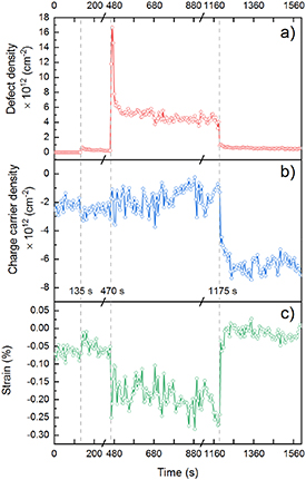
Figure 2. Time-resolved changes in sample properties after plasma exposure and venting to air. Time-dependent (a) defect density, (b) doping density and (c) strain extracted from the Raman spectra with 5 sec. resolution using the procedure described in the text. The time axis is the same as in figure 1(b)
Download figure:
Standard image High-resolution imageAt the beginning of the experiment the defect density is near-zero; pre-strain is low and initial carrier density is ≈ −2.2 × 1012 cm−2, with minus sign corresponding to hole-doping. Both plasma exposure steps change defect density, doping, and strain. The defect density after the second discharge is ≈1.6 × 1013 cm−2 and rapidly (≈50 s) decreases to ≈6 × 1012 cm−2 after the plasma is turned off. Plasma exposures induce n-doping of ≈7 × 1011 cm−2 and strain of ≈0.1%.
After the fast dynamic following the plasma exposures, the sample is stable in argon (pAr = 5 mbar) as the carrier density, strain, and defect density remain stable in the interval t = 520–1170 s. At the time t = 1175 s, we start filling the chamber with air. We observe a rapid decrease of the defect density by an order of magnitude, to ≈5 × 1011 cm−2 within 40 s (figure 2(a)). Simultaneously, we observe p-doping from air exposure, ≈5 × 1012 cm−2 (figure 2(b)), accompanied by the relaxation of strain (figure 2(c)). We note that changes in the carrier density affect the intensity ratio I(D)/I(G) used to extract the defect density [43, 44]. These effects are accounted for in the analysis of figure 2 (supplementary information). Following these initial fast changes, we observe slow dynamics on the time scale of hours. During that time, the defect density decreases by more than a factor of two and the carrier density increases by an order of magnitude (supplementary figure S5).
To summarize our observations so far, the data of figures 1–2 show that in situ plasma-induced defects in graphene are stable in argon but react with air. The density of these defects decreases by an order of magnitude from ≈6 × 1012 cm−2 in argon to ≈5 × 1011 cm−2 in air. However, the question remains: what is the chemical/physical nature of these defects?
In general, the defects produced by plasma exposure [29] can be structural (i.e. missing carbon atom) [24] or functional (sp3-like defects interacting with an external atom/molecule) [2, 32]. These defect types are distinguished by their energy and related stability [24]. To estimate this energy scale, we thermally anneal our samples. Figure 3 shows the evolution of the Raman spectra and calculated defect density for the sample annealed in situ in vacuum right after the introduction of defects. The D mode in figure 3(a) almost completely disappears after a relatively mild annealing at 85 °C, and the apparent defect density drops to the same value as in pristine graphene (figure 3(b)). It is known that structural defects (missing carbon atoms) are stable up to much higher temperatures of 800 °C–900 °C [45, 46]. However, the presence of additional impurity atoms, like carbon [47] or silicon [48] may influence the stability temperature. On the other hand, most of the organic functionalities are known to desorb at temperatures below 100 °C [21, 49, 50]. The strong decrease of the density of defects upon the exposure to ambient points towards their reactivity. This suggest that the defects produced by Ar plasma in our experiment in situ are mainly functional. The remaining concentration of defects after the exposure to ambient suggests that functional defects may have reacted with ambient, whereas the structural defects remained. However, the precise microscopic mechanism should be the subject of future TEM and XPS studies.
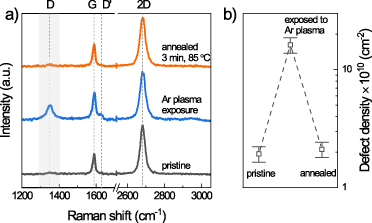
Figure 3. Reversibility of plasma-induced defects upon in situ annealing. (a) Evolution of Raman spectra of graphene. A defect mode appears in pristine graphene (black) upon plasma exposure (blue). After in situ annealing to 85 °C the mode disappears (red). (b) The defect density extracted for each step in (a).
Download figure:
Standard image High-resolution imageTo figure out the type of functional attached to the carbon atoms, we performed DFT calculations of binding energies, induced doping, and strain for H-, OH- and O- functional defects (supplementary figure S6). The lowest binding energy of −0.839 eV as well as induced electron doping and strain below 0.2% qualitatively suggest hydrogen as the most likely defect type induced by Ar plasma in situ at mbar pressures. Indeed, a similar behavior was observed for weakly bound functional defects in hydrogenated graphene [50–52]. In addition, hydrogen functionalities are expected to produce charge transfer and electron-doping [4, 53] similar to the one observed in figure 2(b) as well as induce significant strain[54] due to modification of bond lengths, the behavior is seen in figure 2(c). Finally, while the C-H bond is strong in bulk compounds, it is much more reactive in the case of graphene [4, 33, 55]. Therefore, it is not surprising that H-functionalities are removed from graphene upon exposure to ambient.
There are two possible mechanisms for hydrogen functionalization in our experiments. First, H2 that is present in trace concentrations in our chamber in medium vacuum becomes ionized together with Ar due to similar ionization energies [51] and may react with grapheme [26],52. Second, moisture and hydrocarbons could be adsorbed on our pristine CVD-grown graphene samples during the fabrication [56, 57] and may dissociate under ion/electron bombardment [58]. This could also lead to hydrogen functionalization. We note that more precise analytical techniques such as in situ XPS may distinguish between the proposed scenarios.
One particularly attractive application of reactive plasma-induced functional defects is for the further controlled chemical functionalization of graphene. Hydrogenated graphene is an interesting candidate for further chemical functionalization due to its reactivity [4, 27, 33, 55]. The results above show that plasma-induced defects in graphene react with air. This greatly reduces their density and limits the ex situ functionalization potential. To overcome this limitation, we propose a new in situ functionalization pathway. The idea behind the approach is to introduce target molecular species into a vacuum chamber with freshly in situ Ar-induced functional defects before the defects react with air. We expect that the target species should attach to a large density of 'seed-points' in graphene while these defects are still reactive. In the rest of the paper, we show the proof-of-principle of such two-step functionalization process.
To demonstrate the viability of our approach, we chose ammonia (NH3) as our target functional. The interaction of ammonia with graphene is well understood and is commonly used to introduce a large carrier density in graphene [30, 31, 59], e.g. for applications in transparent conductive electrodes. In a proof-of-principle experiment, we first generated defects using Ar plasma as discussed above (10 s, 1 dBm, 0.1 mbar). In the second step, without breaking the vacuum, we introduced NH3-plasma (15 s, 1 dBm, 0.2 mbar) to functionalize the defects created during the first step. Finally, the sample was exposed to the ambient. Defect density and charge carrier density at each step of the functionalization process are shown in figure 4 (red points). For comparison, in the same graph we show a sample that was exposed to Ar plasma only (15 s, −2 dBm, 5 mbar, green points) and another sample that was exposed to NH3 plasma only (50 s, 2 dBm, 0.2 mbar, blue points).

Figure 4. In situ two-step functionalization of graphene. The carrier density and the defect density shown for each step of the two-step functionalization approach of graphene (red). In that approach, anchor points are created via argon plasma exposure and are functionalized by exposure to NH3 plasma. For comparison, the samples exposed just to Ar plasma (green) and just to NH3 plasma (blue) are also shown. The carrier density shown here is relative to the pristine state, to ease the comparison between the samples.
Download figure:
Standard image High-resolution image
We first examine reference Ar-only and NH3-only samples. In the Ar-only sample, as discussed above in figures 1 and 2, we created the defect density of ≈6 × 1012 cm−2, which induced a slight n-doping of ≈7 × 1011 cm−2 (figure 4, green points). This defect density drops by more than one order of magnitude upon exposure to ambient. In contrast, NH3-plasma exposure generates, by itself, a large n-doping of ≈7 × 1012 cm−2, while generating the defect density of ≈2 × 1011 cm−2 (figure 4, blue points). After exposure to ambient, the concentration of defects is only slightly reduced, while the doping is reduced strongly. Similar results for NH3 samples have been reported previously [29–31, 59]. We conclude that both plasma treatments induce functional defects with different functional groups. The functional groups produced by Ar plasma (likely hydrogen functionalities) induce electron doping and appear to be reactive. In contrast, the groups produced by the NH3 plasma (ammonia) induce electron doping and do not interact with ambient air strongly [24, 29, 31, 59–62]. The hole doping seen in both samples upon air exposure likely results from adsorption of water from ambient.
Finally, we examine the sample exposed to the two-step in situ functionalization process (figure 4, red). The first Ar plasma treatment results in the defect density ≈8 × 1011 cm−2. The following exposure to NH3 plasma during the second step does not change the extracted defect density. Despite that, the carrier density increases to ≈5 × 1012 cm−2. Importantly, the defect density remains near constant upon exposure to ambient. All of that suggests that during the second functionalization step NH3 derivatives bind to the reactive functional 'seed-point' defects in graphene produced by Ar plasma in the first functionalization step (probably forming mostly graphitic-N type of defects [31, 60, 63]) rather than additionally attach directly to graphene. Indeed, if latter was the case, we would expect to see an increase in the defect density upon NH3 plasma exposure in the second step. In addition, the stability of the defect density in the two-step process suggests that functionalization of the defects is stable, unlike the case we observed for Ar plasma, but similar to what we have seen for NH3 plasma. Finally, large electron doping after the two-step process suggests efficient NH3 functionalization. All of that constitutes the proof of principle for our functionalization strategy.
Utilizing in situ functionalization method used here, other organic or inorganic functional can be introduced to graphene [27, 33]. The advantage of this approach is the possibility to create high densities of 'freshly-generated' reactive defects that could generate large doping of >1013 cm−2, facilitate close packing of molecules, and allow the functionalization of graphene with previously inactive reagents.
In summary, we developed a new in situ approach to generate and monitor defects in graphene. We have shown that defects in graphene created via Ar plasma exposure are stable in vacuum but react with the ambient. Both the defect density and the carrier density in graphene decrease by about an order of magnitude upon exposure to ambient. We demonstrated a two-step in situ functionalization of graphene. In this process, we functionalized graphene with NH3 functional at high density utilizing the reactive 'seed-point' defects created via Ar plasma without exposure to ambient. We confirmed the functionalization by continuously analyzing defect density, carrier density, and strain in our samples through in situ Raman spectroscopy. Overall, we believe that our novel in situ functionalization approach using reactive defects opens the possibility to introduce various chemical functionalities to graphene and thereby providing a pathway towards scalable creation of various hybrid organic/inorganic 2D materials.
3. Methods
3.1. Sample synthesis
Single layer graphene is synthesized on the copper substrate by CVD. The mixture of methane (5 sccm), hydrogen (10 sccm), and argon (5 sccm) is let into the CVD chamber, which is kept at 1035 °C. The growth time is 7 min. After the growth, graphene is transferred onto the Si/SiO2 substrate by a standard method [64].
3.2. Setup
The vacuum chamber is pumped down to p ≈ 10–5 mbar. The working gas (Ar or NH3) is let into the chamber with the partial pressures of 0.1–5 mbar. The plasma is generated via capacitive coupling of a top plate electrode and the chamber, using the microwave signal from HP8648B microwave generator at a constant frequency of 13.56 MHz amplified by 50 dB with the amplifier. The chamber is kept at the ground potential. The sample is located at the sample holder halfway between the electrode and the bottom of the chamber. The sample holder is electrically isolated from the electrode and the ground. No additional bias potential was used. The sample holder is electrically contacted for in situ annealing purposes. The concentration of defects in graphene can then be controlled by adjusting the discharge power and plasma exposition time. The sample is monitored with in situ Raman spectroscopy in a modified Witec Alpha setup using 532 nm excitation wavelength.
3.3. DFT calculations
DFT calculations are carried out with the all-electron code FHI-aims [65]. Geometry optimization is performed within the generalized gradient approximation for the exchange-correlation functional using the Perdew–Burke–Ernzerhof parametrization [66]. Van der Waals interactions are included with the Tkatchenko-Scheffler scheme [67]. We employ tight integration grids and TIER2 basis sets [68], and the atomic positions are relaxed until the Hellmann-Feynman forces are smaller than 10–3 eV/Å.
Acknowledgments
We gratefully acknowledge Dr. Georgy Gordeev for useful discussions. This work was supported by the Deutsche Forschungsgemeinschaft (DFG)—Projektnummer 182087777—SFB 951 and ERC Starting Grant No. 639739. A.M.V and C.C. acknowledge financial support from the German Federal Ministry of Education and Research (Professorinnenprogramm III) as well as from the State of Lower Saxony (Professorinnen für Niedersachsen).