

Abstract
This paper reports on design, measurement and optimisation of a Tamm plasmon metal-distributed Bragg reflector (DBR) cavity for use in the green part of the visible spectrum. It uses an optimised silver layer thickness and a porous DBR created using a novel electro-chemical etching technique. This device has applications in low-cost lasers, photodetectors, and photoconductive switches for the visible wavelength range.

Original content from this work may be used under the terms of the Creative Commons Attribution 4.0 license. Any further distribution of this work must maintain attribution to the author(s) and the title of the work, journal citation and DOI.
1. Introduction
Distributed Bragg reflectors (DBRs) are essential components for the development of optoelectronic devices that are formed from multiple layers of alternating materials with varying refractive index. Vertical-cavity surface-emitting lasers (VCSELs) traditionally consist of a lower and an upper DBR mirror, sandwiching an active/confinement layer containing multiple quantum well's (MQWs). In this paper, we focus on the possibility of substituting the upper DBR mirror of a traditional VCSEL by using Tamm Plasmon confinement. Tamm plasmons, or Tamm optical states, are the photonic equivalent of electronic Tamm [1] states that occur due to the termination of that lattice. These surface states are formed when a one-dimensional photonic crystal, a Bragg stack, is terminated by a metal layer. The resulting sub-wavelength cavity can be tuned by controlling the thickness of the metal layer [2–6] or by the 'spacer' layer, the upper most layer of the Bragg stack. By patterning the metal surface, it is possible to create confined Tamm plasmons [7]. In doing this, we have built upon existing theoretical research proposed by Zheng et al [8] to realise such a cavity in the technologically important GaN system. This has been challenging up to now due to the low refractive-index contrast between AlN and GaN and also the large lattice-mismatch between AlN and GaN of around 2.5% [9], both making it difficult to achieve DBRs with a high reflectance and also to maintain a good crystal quality which is important for the subsequent growth of a micro-cavity. It should be noted that InAlN/GaN layers are an alternative approach which can achieve lattice matching and high reflectance [10, 11].
Recent advances in the fabrication of lattice-mismatched DBRs based on GaN/nano-porous GaN DBRs have shown high reflectance, R > 99.5% [12, 13] due to much higher refractive-index contrast between GaN and nano-porous GaN. Figure 1 shows a schematic of the structure we are considering here, the higher refractive contrast makes the Tamm plasmon achievable in only 11 periods, many fewer than used in similar devices [7] and that theoretically proposed in [8].

Figure 1. A schematic illustration of the epitaxially grown base structure on a sapphire substrate—this consists of a GaN growth layer (GaN_GL), 11-period DBR, GaN spacer layer (thickness = T_GaN_SL), and silver layer (thickness = T_Ag).
Download figure:
Standard image High-resolution imageThe simplicity of the Tamm structure in terms of growth time not only reduces the fabrication cost since only one DBR is required, it also allows for post growth tuning with the metal layer thickness. Recently a similar GaN Tamm cavity has been published [14], the work presented here was carried out independently to that work and explores the Tamm resonance dependence to Ag thickness in experimental results. This shows the great level of interest in Tamm modes for making short wavelength devices not only for VCSELs but also for photodetectors and photoconductive switches [15]. This technology could also be combined with emerging GaN integrated photonic devices [16, 17].
2. Fabrication of porous GaN DBR
The sample is grown on (0001) sapphire substrates using a low-pressure metal-organic-vapour phase epitaxy system by means of a standard two-step growth method. After the substrate is initially subjected to thermal cleaning in flowing H2, a low-temperature GaN nucleation layer with a thickness of 25 nm is prepared, followed by a 1.6 µm GaN layer grown at 1100 °C. Subsequently, 11 pairs of undoped GaN and heavily silicon doped n-GaN are then grown, where the thicknesses of the undoped and the n-GaN in each pair are 50 nm and 65 nm, respectively, and the doping level is on a scale of 1019 cm−3. A microcavity structure is then grown, and it consists of a 54 nm undoped GaN layer, 3 pairs of InGaN/GaN MQW and a further 54 nm undoped GaN layer. For the InGaN MQWs, the thicknesses of the InGaN quantum well (QW) and GaN barrier are 2.5 nm and 10 nm, respectively, and the indium content is ∼20%. Finally, the 11 pairs of undoped and n-GaN layers are formed into nanoporous DBRs by an electro-chemical (EC) etching technique—similar procedures have been proposed by Zhang et al [12] and Zhu et al [13].
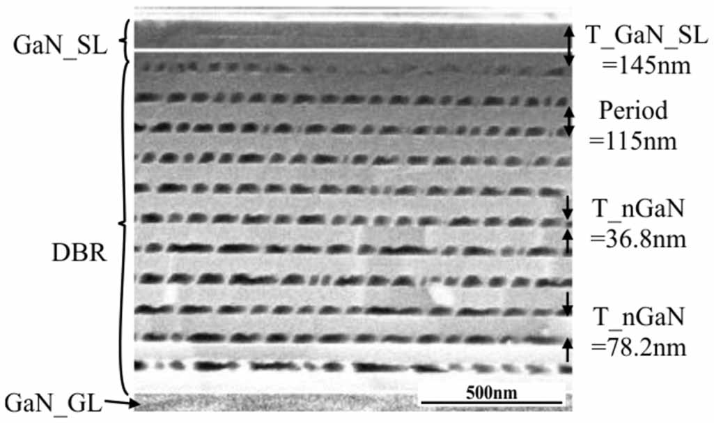
The mechanism of EC etching is based on a combination of an oxidation process and then a dissolution process in acidic solution under an anodic bias. Under a positive anodic bias, the injection of holes leads to the oxidation of GaN, and the oxidized layer is then chemically dissolved in an acidic electrolyte. Therefore, EC etching can only be performed on n-type GaN with high conductivity. In this case, n-GaN can be etching into a nanoporous structure whose refractive index depends on porosity, while undoped GaN remains unetched. No trench etching was necessary to aid porosification of buried n-GaN layers due to small dimensions of the samples. To realise VCSEL arrays on a wafer scale then trench etching would be a necessary added step. Our EC processes are carried out in nitric acid with a mole concentration of 0.5 M as an electrolyte at room temperature, where n-doped GaN is used as an anode and a platinum foil as a cathode. The EC porosification process is carried out with a DC bias of 9 V bias until the etching current drops to zero, which means that all the n-GaN layers have been etched into nanoporous GaN layers—for further details please refer to our previously published paper, Hou et al [18]. Not all of the n-GaN was converted porous during the EC etching process (further investigation is on-going), so in the simulations that follow a ratio (r) of 0.32 was used for porous (36.8 nm)/non-porous (78.2 nm) layers, which was measured from the SEM image shown in figure 2. The etched layer morphology is on the boundary of mesoporous/macroporous given the large width of the pores. Following the EC etching, firstly a 70 nm thick layer of Ag has been evaporated onto the surface of the top GaN spacer layer.

Figure 2. An SEM image of the etched porous layers.
Download figure:
Standard image High-resolution image3. Simulation and measurement of optical behavior
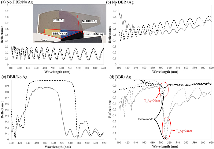
A two-dimensional finite difference time domain (FDTD) approach has been used to simulate the multilayer structure using commercial-grade software (Lumerical Solutions, Inc., www.lumerical.com/tcad-products/fdtd/). A broadband plane-wave source is incident onto the top of the structure, first passing through the 70 nm thick Ag layer before impacting the 145 nm thick GaN spacer layer and DBR structure—period (a) 115 nm (11-periods). Beneath the DBR, there is a 1.6 µm thick GaN growth layer on a Sapphire substrate. The pores are modelled by adding blocks of air of random width to approximate the dimensions shown in figure 2—the thicknesses of nanoporous n-GaN and undoped GaN are 36.8 nm and 78.2 nm respectively. Given their thin vertical dimension, the QW layers are deemed to have negligible effect on the reflectance and are not added to the simulation structure. The refractive index for the all GaN material used in simulations was n = 2.427 at λ = 510 nm [19] and material data for the 'Ag (Silver)—CRC' were fitted to our spectral region of interest within Lumerical. The grown sample has four regions of interest mapped out in figure 3(d). There are two distinct areas, one with the EC etched DBR and one unetched. Both areas are partially masked and 70 nm of Ag being evaporated onto the surface, gives four regions on the sample shown in the inset. A direct wide-angle measurement of the four regions is carried out using Fourier image spectroscopy (FIS) [20]. A white-light source is incident on the sample surface through, and collected by, the same high numerical-aperture (NA = 0.8) 100× magnification microscope objective. The back focal-plane of this objective is scanned, which allows full angular reflection data from the sample, normalised to that of a silver mirror, to be plotted against wavelength.
Figure 3. FDTD simulated (dashed lines) and FIS measured normal to the interface (solid lines) reflectance from the four regions of the sample—a photo of which is shown in the inset—(a) No DBR/No Ag, (b) No DBR + Ag (24 nm thickness), (c) DBR/No Ag, (d) DBR + Ag (24 nm and 70 nm thicknesses).
Download figure:
Standard image High-resolution image
The normal incidence reflectance from these four regions is captured between λ = 400 and 620 nm and are plotted using dashed lines for FDTD simulations and solid lines for FIS measurements in figure 3. The unetched/uncoated region (No DBR/No Ag—plot (d)) shows a rippled reflectance centred at ∼0.2 with a ripple period between 10 and 20 nm depending on spectral position. This is consistent with what one would expect for constructive/destructive interference between the GaN/air and GaN/Sapphire boundaries. When coated with Ag (No DBR + Ag—plot (b)), the reflectance increases due to the high reflectance of Ag, but due to its thin-film nature it is still relatively transparent at these wavelengths—the ripple period however does not change. Large reflectance above 0.99 is predicted in simulations from the DBR (DBR/No Ag—plot (c)) with a reflectance bandgap ranging from λ = 432–553 nm (FWHM). The porous regions are approximated to be perfect polygons in the FDTD simulations, therefore there is near-ideal Bragg reflection from the multiple layers. Irregular porous shapes introduce scattering, so the etched structure is no longer a perfect Bragg reflector and the overall peak measured reflection drops to ∼0.88 in the measurements. To achieve lasing, it would be necessary to increase the number of layers to achieve reflectivity ∼0.99 (∼25 pairs, as has recently been demonstrated at room temperature in the AlGaAs system [21]). A further important factor from the measurement is that the illumination covers a large angle even though we are only considering the reflected light normal to the surface. Reduction of DBR peak reflectivity and some blueshift of resonance is expected off normal axis causing a broadband drop in reflection. When the structure shown in figure 2 is coated with 70 nm of Ag (DBR + Ag—plot figure 3(a)) a small dip is seen in the reflectance at around 505 nm caused by Tamm mode confinement at this wavelength. The strong increase in reflectance caused by the TAMM mode is present at all angles collected by the high-NA objective (not shown), with only very small variations in bandwidth and intensity. There is a blue-shift of approximately 30 nm in the Tamm mode wavelength at the highest collection angles (θ ≈ 53°, where normal reflectance is θ = 0°) caused by a change in the layer thicknesses seen by the light at these higher angles. We believe that the results would be the same for a smaller-magnification/lower-NA objective that would illuminate a significantly larger area. Our FDTD modelling predicted that by moving to T_Ag = 24 nm, a much larger dip would be obtained. The 70 nm Ag was removed and replaced by a thinner layer which we estimated to be in the region of 24 nm. Figure 3(a) shows that a good level of agreement is obtained between the measured and modelled cases. We believe the differences are primarily caused by the scattering discussed above. We demonstrated the Tamm plasmon for two different metal thickness: however, the GaN spacer layer thickness and the DBR thickness were determined by the GaN growth conditions described earlier. The Tamm mode does not occur at the centre of the DBR stopband: this arises from the symmetry breaking of the spacer layer, and can be seen in [2–5, 7, 13, 14].
4. Conclusion
We have demonstrated through numerical modelling and fabrication a Tamm mode resonance in a silver coated GaN/Porous GaN Bragg reflector structure. In future, careful design, that overlaps QWs spatially with the regions of highest electric field intensity and spectrally with the resonance could enable novel LED and laser devices to be fabricated [21].
Acknowledgments
This work was supported by the Engineering and Physical Sciences Research Council through the Programmes Manufacturing of nano-engineered III-nitride semiconductors (Grant No. EP/M015181/1) and Future Compound Semiconductor Manufacturing Hub (Grant No. EP/P006973/1).