


Abstract
The noise performance of integrated low noise amplifiers (LNAs) is impaired by on-chip inductors owing to their low-quality factor, especially when inductors are used in the signal path at the input, such as for the inductively degenerated common-emitter amplifier. The inductively degenerated common-emitter configuration is largely used in LNA design, owing mainly to its ability to achieve impedance and noise matching simultaneously. This paper proposes an LNA configuration that achieves impedance matching and noise matching simultaneously without an inductor in the input signal path, owing to capacitive feedback and transistor sizing. Only the resistive component of the optimum noise resistance is matched to the source resistance. The impact of the mismatch due to the reactive component to the noise figure is reduced by the ratio Gs/Rn. A technique initially developed for the broadband matching of a single-layer microstrip patch antenna is used for the output matching network. Using a 130 nm silicon–germanium heterojunction bipolar transistor process, simulation results indicate a noise figure of 2.3 dB, a gain of 26 dB and S11 and S22 that are better than −12 dB at 1.42 GHz. This frequency corresponds to the 21 cm hydrogen line. This novel multi-stage LNA can be used for the detection of electromagnetic radiation from neutral hydrogen atoms from space in radio astronomy and the proposed design methodology can be generalized to LNAs.
Export citation and abstract BibTeX RIS
1. Introduction
The matching of the input impedance of a low noise amplifier (LNA) to the impedance of the source reduces signal reflections at the input and improves the gain, the signal-to-noise ratio (S/N) and the linearity of the amplifier (Fu et al. 2010). Impedance matching is achieved when the source impedance is equal to the complex conjugate of the input impedance. The S/N at the output is related to the noise figure (NF) of the LNA and, for a given operating frequency, the NF is minimal when noise matching is achieved. At noise matching, the optimum noise impedance of the LNA is equal to the impedance of the signal source. Hence, to achieve the optimum S/N and sensitivity, both input impedance and noise impedance must be matched to the source impedance (Fu et al. 2010). Such matching can be achieved when the inductively degenerated common-emitter (CE) or common-source is used for the first stage of the LNA. For simultaneous impedance and noise matching an inductor is required at the input of the LNA in the base circuit of the first stage. This is known to achieve the best noise and linearity performance (Aparin & Larson 2003). However, integrated spiral inductors have a low-quality factor Q, with a typical value close to 15, in contrast with external inductors having a Q factor that can reach 150 and more. Therefore, the thermal noise due to the base input inductor is significant when compared to the input signal and impairs the noise performance of the LNA. The thermal noise of the inductor resistance adds to the base parasitic resistance of the input transistor, which is known to be a significant noise contributor to an LNA. To prevent the performance degradation caused by the on-chip spiral inductor, a high Q external inductor can be used. Although such a solution has been proposed in Belostotski & Haslett (2007) and Bimana & Sinha (2016), in achieving sub-1 dB NFs, it is desirable to reduce the number of external components for an integrated receiver to the minimum possible. Such a reduction lowers the cost and size of the receiver.
This paper investigates and proposes a new design for an integrated LNA operating in the frequency band of 1.400–1.427 GHz. This band is allocated by the International Telecommunication Union to radio astronomy and corresponds to the electromagnetic radiations of the neutral atomic hydrogen (H i) received on earth (ITU 2013). Hydrogen, which is the most abundant element in the universe, constitutes 75% of its mass. At very low temperature (100 K) in the interstellar space, the proton and the electron of the hydrogen atom can spin in the same or opposite directions along their individual axes, corresponding to different energy levels. A change in the spin direction and the energy level corresponds to the emission of photons at 1.420 GHz, the 21 cm hydrogen line (Saje & Vidmar 2017). However, because of the large recession velocities of galaxies, photon emissions are Doppler shifted to lower frequencies, hence the frequency band. The distribution of H i arising from radio observations allowed astronomers to locate the center of our galaxy, the Milky Way, and its spiral arms. By observing H i emissions, the characteristics of some elements of the universe, such as their velocity and their mass, can be studied.
A CE transistor with capacitive feedback is used as the input stage. The capacitive feedback and the capacitive load of the input transistor achieve a quasi-resistive input impedance at 1.420 GHz, without an integrated inductor in the base and emitter circuits. A cascode configuration for the output stage is used to improve the isolation between the output of the LNA and its input. The output stage drives an output circuit that matches the output impedance of the last stage of the LNA to the 50 Ω load in the operating bandwidth.
This paper is structured as follows: Section 2 presents the input stage of the proposed LNA and demonstrates that, under specific conditions, the imaginary part of the input impedance of the stage can be neglected. The section is divided into three sub-sections addressing the capacitive feedback circuit, the impact of the feedback on noise performance and the implementation of the capacitive load of the input stage. Section 3 discusses the dependencies of the optimum noise resistance. Section 4 describes the output matching network of the LNA and derives design equations used to determine the values of its capacitive and inductive components. Section 5 presents the topology of the LNA and discusses its design. Sections 6, 7 and 8 provide simulation results, the design methodology, and the conclusion, respectively.
2. The Input Stage
2.1. The CE With Capacitive Feedback
It is well known that the noise performance of an amplifier is mainly determined by its first stage. Therefore, a high gain and a low NF are desired for the first stage of the LNA. Capacitive feedback is reported in several LNA designs. In Kang et al. (2011) and Liu et al. (2018) capacitive feedback is used to reduce the size of the emitter inductor, to improve linearity and to match the input resistance to the optimum noise resistance of an inductively degenerated CE input stage of an LNA. To reduce the chip size and to avoid using small, inaccurate degeneration inductances, the source inductor is replaced by capacitive feedback but the gate inductor is maintained for noise matching in Tran et al. (2011) and Wu & Shahroury (2006). In Howard & Cressler (2009), shunt capacitive feedback is used to increase the bandwidth of an LNA in reducing the Q factor at the input. The use of a noiseless capacitor to close the feedback loop achieves input impedance matching without impairing the NF of this stage. Although this can be predicted intuitively, the effect of the capacitive feedback on noise parameters is evaluated in the following paragraphs. The CE input transistor with capacitive feedback and capacitive load is represented in Figure 1, where vin and vout are the input and output signals, respectively, Cf is the feedback capacitor and CL is the capacitive load.

Figure 1. The CE with capacitive feedback and capacitive load.
Download figure:
Standard image High-resolution imageThe circuit in Figure 1 represents a shunt-shunt feedback network and can be analyzed using feedback theory. If zi and zo are the input and output small-signal impedance, respectively, of the basic amplifier in Figure 1 without feedback, the input and output small-signal impedance with feedback Zi and Zo , respectively, are given by (Gray & Meyer 2010):


where T is the loop gain, with  , α being the transresistance and β the feedback transconductance. The transresistance α and the feedback transconductance β can be determined using the representation of the shunt-shunt feedback network in Gray & Meyer (2010) and the simplified small-signal model of Figure 1, where the capacitive feedback Cf
is not included. This small-signal model is shown in Figure 2, where Cbe is the base-emitter capacitance, Cbc the base-collector capacitance and gm
the transconductance of Q1.
, α being the transresistance and β the feedback transconductance. The transresistance α and the feedback transconductance β can be determined using the representation of the shunt-shunt feedback network in Gray & Meyer (2010) and the simplified small-signal model of Figure 1, where the capacitive feedback Cf
is not included. This small-signal model is shown in Figure 2, where Cbe is the base-emitter capacitance, Cbc the base-collector capacitance and gm
the transconductance of Q1.

Figure 2. Small-signal model of the CE with capacitive loading.
Download figure:
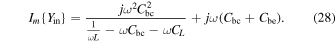
Standard image High-resolution imageThe input impedance zin of Figure 2 is given by (3)
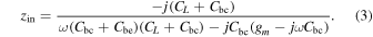
When the feedback capacitor Cf is added, the feedback transconductance β is given by (4)

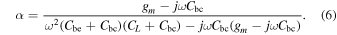
The transresistance α is given in (5) and can be re-written as (6)

Assuming that  , (1) can be simplified and the input impedance of Figure 1 is given by (7)

The input impedance has an imaginary component that can be neglected when  .
.
Under this condition, the input impedance becomes:

Equation (8) shows that, under the conditions that  and
and  , the input impedance is real, not related to the operating frequency and can be equal to 50 Ω, the internal resistance of the source. However, it is desired to investigate under what conditions
  . The inverse of T is given by (9)
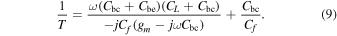

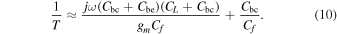
Reporting the unity frequency fT
in (10), with  , yields (11)
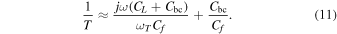
The base-collector capacitance Cbc is generally small, compared to Cf
, therefore  and (11) yields (12)

Because  and
and  ,
,  and the conditions to achieve a real input impedance for the input stage in Figure 1 are summarized as follows:
- (a)

- (b) (this is generally the case)
- (c)
- (d).


Conditions (b) and (d) indicate that Cbc must be considerably small, compared to Cf and CL . These conditions are best met by integrated rather than by discrete transistors because Cbc is related to the size of the transistor. Condition (c) shows that the operating frequency f may be required to be much lower than fT , which means that a high fT is needed for a low operating frequency, limiting the maximum operating frequency. Conditions (a), (b), (c) and (d) are stringent but can be slightly relaxed, as shown in Section 2.3.
2.2. Noise Parameters of The CE with Capacitive Feedback
The impact of the capacitive feedback and load on the noise parameters of the circuit represented in Figure 2 can be analyzed by the noise correlation matrix theory (Rothe & Dahlke 1956). Although it can be concluded intuitively that the NF of the input stage of the LNA is unchanged because the capacitive feedback and load are noiseless, the impact of these noiseless components on the Ysopt is not trivial. For the analysis of this impact, the circuit in Figure 1 is decomposed into three sub-circuits: the first sub-circuit is the CE transistor, the second sub-circuit is the capacitive load CL and the third sub-circuit is the feedback capacitor Cf .
It can be shown that the noise correlation matrix of the CE two-port network is given by (Moura & Darwazeh 2005):
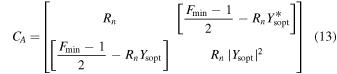
where Fmin is the minimum possible noise factor, Rn is the noise resistance and Ysopt is the optimum source admittance.
The LNA can be represented as a cascade of two two-port networks represented in Figure 3, where the CE transistor and CL constitute the first stage of the LNA without feedback.

Figure 3. Input CE and capacitive load as a cascade network.
Download figure:
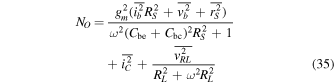
Standard image High-resolution imageAssuming that the noise due to the second stage and the output matching network can be neglected, the noise factor of the first stage is given by:
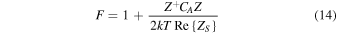
where CA
is the noise correlation matrix of Q1 and CL
cascaded, Zs
is the impedance of the source,  is the Hermitian conjugate of Z with
 ![$Z=\left[\begin{array}{c}1\\ {Z}_{s}^{* }\end{array}\right]$](https://content.cld.iop.org/journals/1538-3873/133/1019/015001/revision2/paspabc9a5ieqn18.gif) . The Hermitian conjugate
. The Hermitian conjugate  is obtained by transposing Z and converting its elements in their complex conjugates. The noise correlation matrix CA
of two two-port networks in cascade is expressed as:
is obtained by transposing Z and converting its elements in their complex conjugates. The noise correlation matrix CA
of two two-port networks in cascade is expressed as:

where A1 is the transmission matrix of the input two-port network and CA1 is its noise correlation matrix. CA2 is the noise correlation matrix of the two-port network formed by CL .
The noise correlation matrix CA2 is nil, as its diagonal terms are real values that represent the power spectrum of each noise source and the off-diagonal terms represent their cross-power spectra; these terms are nil for a noiseless network. The noise correlation matrix of the input stage is given by (16)
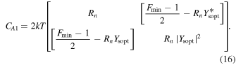
It is then concluded that CA is not related to CL , hence CA = CA1 and noise parameters Fmin, Rn and Ysopt are independent from CL .
The impact of Cf on the noise parameter of the input transistor can be investigated in decomposing the CE with feedback in two two-port networks in parallel. The first two-port network is the CE stage, with CA1 as its noise correlation matrix, in chain representation. The second two-port network is the feedback capacitor, with CA3 as its noise correlation matrix, in chain representation. The resulting decomposition is shown in Figure 4.

Figure 4. CE transistor and Cf as parallel two-port networks.
Download figure:
Standard image High-resolution imageIt can be shown that if CY is the noise correlation matrix of the network in Figure 4, then CY is given by:

where CY1 and CY3 are the transformation of CA1 and CA3 in the admittance representation.
The resulting noise parameters are derived from the transformation of CY into the chain representation. The transformation of CA1 in CY1 is done by the congruence transformation in (18):

where T is the transformation matrix and T+ its Hermitian transform.
Similarly, the transformation of CA3 into CY3 is given by (19):

The transformation of CY
into  is done by the expression:

The noise correlation matrix transformations represented by [T] are given in Table 1 (Moura & Darwazeh 2005).
Table 1. Transformation of Noise Correlation Matrices
| Transformed | Original Representation | |||
|---|---|---|---|---|
| Representation | CY | CZ | CA | CH |

|
![$\left[\begin{array}{cc}1 & 0\\ 0 & 1\end{array}\right]$](https://content.cld.iop.org/journals/1538-3873/133/1019/015001/revision2/paspabc9a5ieqn22.gif)
|
![$\left[\begin{array}{cc}{Y}_{11} & {Y}_{12}\\ {Y}_{21} & {Y}_{22}\end{array}\right]$](https://content.cld.iop.org/journals/1538-3873/133/1019/015001/revision2/paspabc9a5ieqn23.gif)
|
![$\left[\begin{array}{cc}-{Y}_{11} & 1\\ -{Y}_{21} & 0\end{array}\right]$](https://content.cld.iop.org/journals/1538-3873/133/1019/015001/revision2/paspabc9a5ieqn24.gif)
|
![$\left[\begin{array}{cc}-{Y}_{11} & 0\\ -{Y}_{21} & 1\end{array}\right]$](https://content.cld.iop.org/journals/1538-3873/133/1019/015001/revision2/paspabc9a5ieqn25.gif)
|

|
![$\left[\begin{array}{cc}{Z}_{11} & {Z}_{12}\\ {Z}_{21} & {Z}_{22}\end{array}\right]$](https://content.cld.iop.org/journals/1538-3873/133/1019/015001/revision2/paspabc9a5ieqn27.gif)
|
![$\left[\begin{array}{cc}1 & 0\\ 0 & 1\end{array}\right]$](https://content.cld.iop.org/journals/1538-3873/133/1019/015001/revision2/paspabc9a5ieqn28.gif)
|
![$\left[\begin{array}{cc}1 & -{Z}_{11}\\ 0 & -{Z}_{21}\end{array}\right]$](https://content.cld.iop.org/journals/1538-3873/133/1019/015001/revision2/paspabc9a5ieqn29.gif)
|
![$\left[\begin{array}{cc}1 & -{Z}_{12}\\ 0 & -{Z}_{22}\end{array}\right]$](https://content.cld.iop.org/journals/1538-3873/133/1019/015001/revision2/paspabc9a5ieqn30.gif)
|

|
![$\left[\begin{array}{cc}0 & {A}_{12}\\ 1 & {A}_{22}\end{array}\right]$](https://content.cld.iop.org/journals/1538-3873/133/1019/015001/revision2/paspabc9a5ieqn32.gif)
|
![$\left[\begin{array}{cc}1 & -{A}_{11}\\ 0 & -{A}_{21}\end{array}\right]$](https://content.cld.iop.org/journals/1538-3873/133/1019/015001/revision2/paspabc9a5ieqn33.gif)
|
![$\left[\begin{array}{cc}1 & 0\\ 0 & 1\end{array}\right]$](https://content.cld.iop.org/journals/1538-3873/133/1019/015001/revision2/paspabc9a5ieqn34.gif)
|
![$\left[\begin{array}{cc}1 & {A}_{12}\\ 0 & {A}_{22}\end{array}\right]$](https://content.cld.iop.org/journals/1538-3873/133/1019/015001/revision2/paspabc9a5ieqn35.gif)
|

|
![$\left[\begin{array}{cc}-{h}_{11} & 0\\ -{h}_{21} & 1\end{array}\right]$](https://content.cld.iop.org/journals/1538-3873/133/1019/015001/revision2/paspabc9a5ieqn37.gif)
|
![$\left[\begin{array}{cc}1 & -{h}_{12}\\ 0 & -{h}_{22}\end{array}\right]$](https://content.cld.iop.org/journals/1538-3873/133/1019/015001/revision2/paspabc9a5ieqn38.gif)
|
![$\left[\begin{array}{cc}1 & -{h}_{11}\\ 0 & -{h}_{21}\end{array}\right]$](https://content.cld.iop.org/journals/1538-3873/133/1019/015001/revision2/paspabc9a5ieqn39.gif)
|
![$\left[\begin{array}{cc}1 & 0\\ 0 & 1\end{array}\right]$](https://content.cld.iop.org/journals/1538-3873/133/1019/015001/revision2/paspabc9a5ieqn40.gif)
|
Download table as: ASCIITypeset image
For the determination of CY3, y11 and y21 are required for the feedback network, represented in Figure 5.

Figure 5. Representation of the CL feedback network.
Download figure:
Standard image High-resolution imageThe representation of the feedback network is described by (21) and (22)


It is found that  ,
,  ,
,  ,
,  .
.
Because the feedback two-port network is noiseless, CA3 is nil, the noise correlation matrix of Figure 4 in y-representation is given by (23), derived from (17):

The transformation of CY from (23) in chain representation is given by (24)

where [T] is the matrix required for a congruence transformation from the y-representation to the chain representation.
Equation (24) shows that noise parameters Fmin, Rn , and Ysopt are not affected by the feedback capacitor Cf , as also shown in Kang et al. (2011). However, the capacitive load reduces the phase margin, which can cause instability.
2.3. DC Biasing of the Input Stage
For DC biasing, two options can be considered: a resistor or an inductor in parallel with a capacitor. The first configuration is unwanted because the additional thermal noise from the resistor will impair noise performance. The second configuration consists of an LC tank circuit that can be used as a capacitive load for frequencies that are higher than its resonant frequency. The LC tank circuit achieves a better bandwidth than a shunt RC load (up to 70%) and the LC tank circuit thermal noise voltage due to the parasitic resistance of the inductor is not multiplied by the Q factor, as it should have been at resonance (Simpson 1974).
The impedance of the tank circuit is given by:

where L and CL are the inductor and the capacitor of the tank circuit and ω is the angular operating frequency.
The impedance ZL
is capacitive for  , which is equivalent to
  , where
  is the resonant frequency of the LC circuit, with
  .
.
The equivalent capacitor of the tank circuit for  , is given by (26)

The equivalent load capacitance Ce varies with frequency, indicating from (8) that input impedance matching is only achieved in a narrow bandwidth.
2.4. Impact of the LC Load Circuit on the Input Impedance
The approximation of the input impedance in (8) assumes that the load of Q1 is capacitive. However, when ω is close to ωo , the impedance of the tank circuit is large; it is required to evaluate how the input impedance varies. The small-signal model of the input stage without feedback but with an LC load is represented in Figure 6.

Figure 6. Small-signal model of Q1 with LC load.
Download figure:
Standard image High-resolution imageThe input admittance of Figure 6 is given by (27):

where L is the inductance of the tank circuit and CL its capacitance.
The imaginary part of Yin is given by the expression:
The value of ω for which (28) is nil is given by:

Adding Cf
in parallel with Cbc for feedback and considering that  , yields:

Assuming that  , the angular frequency for which the imaginary part of Yin is nil is given by (31)

Equation (31) shows that the input impedance is real at fo
, the resonant frequency of the LC tank circuit, if  and
and  . Therefore, the imaginary part of the input impedance is small and negligible at frequencies close to fo
; the matching conditions (a), (c) and (d) in 2.1 are relaxed and the new conditions arising are
. Therefore, the imaginary part of the input impedance is small and negligible at frequencies close to fo
; the matching conditions (a), (c) and (d) in 2.1 are relaxed and the new conditions arising are  and
and  , the last-named being equivalent to b). Both conditions can be generally satisfied, especially for integrated circuits.
It can be shown that the input impedance is approximated by (32), derived from (27), where the imaginary part is nil

At fo , (32) becomes (33), which shows that the input impedance is only related to gm when the LC tank circuit is at resonance

3. Dependencies of the Optimum Noise Impedance
It is desired to investigate how the optimum noise impedance can be made to match the source impedance to improve the NF. Noise sources of Figure 1 are shown in Figure 7, where the emitter parasitic resistance is neglected and the inductor of the output LC tank is L and RL is its parasitic resistance. The thermal noise generated by RL is represented by vRL . The feedback capacitor is Cbc. The capacitor of the LC tank is not represented because the output is shorted to evaluate the output noise current io .

Figure 7. Noise sources of the input stage.
Download figure:
Standard image High-resolution imageThe collector and base shot noises are respectively ic
and ib
. The base parasitic resistance is Rb
and the source resistance is Rs
. Hence, the thermal noise voltages due to Rb
and Rs
are vb
and rs
, respectively. Because the sum of i1, i2,  and i4 is nil, the voltage at the base due to the noise sources is:

The total output noise is given by:
where  ,
,  ,
,  ,
,  and
and  are respectively the noise density powers of the base shot noise, the base resistance thermal noise, the source thermal noise, the collector shot noise and the output inductor thermal noise.
The noise to the output due to the source only is given by:
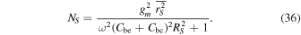
The noise factor F of the first stage is given by (37)

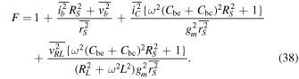
The optimum noise resistance Rsopt is obtained by equating the partial derivative of F with respect to the source resistance ( ) to nil and replacing noise sources by their values:
  ,
,  ,
,  ,
,  , where IB
is the base bias DC current, IC
the collector bias DC current, with
, where IB
is the base bias DC current, IC
the collector bias DC current, with  , k the Boltzmann constant and T the temperature in Kelvin.
The optimum source resistance is provided by (39)
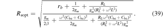
Equation (39) becomes (40) when the output inductor is assumed to be noiseless
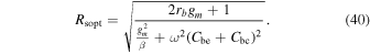
Because  and
and  , (40) can be approximated by (41). Expression (41) is also found in Nyssens (2016)

The expression of Zsopt in Niknejad & Hashemi (2008) for the CE bipolar transistor is:
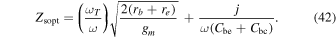
In Niknejad & Hashemi (2008), the NF is derived from noise sources referred to the input. The voltage and current noise source referred to the input are correlated and this correlation is accounted for in further calculations. The approach used in this work aims to avoid the complexity resulting from the calculations related to the correlation between the noise voltage and the noise current referred to the input (Hillbrand & Russer 1976) and leads to (41). However, for collector currents in the range of 2 mA or less, the term in  can result in significant deviations, when (41) and (42) are compared. Elaborated expressions of Rsopt and Xsopt are provided in Voinigescu et al. (1997).
Equations (41) and (42) show that Rsopt can be made to match the source resistance in varying gm , hence the collector current. Because the best noise performance of the transistor is achieved at a constant collector current density (Chen et al. 2004), gm is set in varying the length of the emitter.
From the two-port noise model, noise matching is achieved when Zs = Zsopt, as shown in (43), where Fmin is the minimum possible noise factor, Gs the source admittance, Rn the noise resistance and Zs the source impedance

The expression of the noise resistance is given in (44)

Equation (42) shows that Zsopt has an imaginary component; hence the second part of (43) is not nil. However, the impact of this mismatch to (43) is reduced when Rn is large. As shown in (44), a large Rn corresponds to a small collector current. As elegantly demonstrated in Fu et al. (2010), an inductor in the base signal part can be used to cancel this imaginary part. However, this research seeks to avoid using such an inductor.
4. The Output Matching Circuit
The design of matching networks can be a tedious task for wideband networks and non-standard input and output impedances. For simple problems, such as narrow-band matching, the analytic theory related to impedance matching can be used. However, for wideband matching, the analytic theory is complex and may not provide a solution. Also, solutions found can be sub-optimal and can lead to circuits that are difficult to implement (Yarman 2008). Hence, impedance matching is not a methodical and efficient process when computer-aided tools—based on the brute force technique or the real frequency technique—are not used because the process depends on impedances to match and is based on trial and error (Sharma 2011).
The matching network used is a 4th order circuit, where the parallel RLC components correspond to an SLMPA in the technique by Anguera et al. (2001) and Andújar et al. (2010). In the proposed LNA, the parallel RLC components are connected between the collector of the output transistor and the power supply and serve for DC biasing and for impedance matching. The inductor Lo and the capacitor Co , with the parallel RLC components, constitute the matching circuit.
The LNA is followed by another block and it is desired to match its output to the input impedance of the block and of the measuring test equipment. This impedance is expected to be 50 Ω and the 4th order output matching circuit is proposed at the output of the LNA. For this circuit, the technique used by Anguera et al. (2001) and Andújar et al. (2010) is expanded in this paper. This technique was initially developed to improve the bandwidth of the single-layer microstrip patch antenna (SLMPA) and is based on the equivalent circuit in Figure 8, where the parallel RLC components model the SLMPA and Lo and Co are matching components. It is found in Pues & Van De Capelle (1989) that the radiation pattern of an SLMPA is unchanged for frequencies that are within 10% to 20% of the resonant frequency of the antenna. Therefore, the bandwidth of the SLMPA improves when the relevant matching circuit is inserted between the antenna and the transmitter. Power flows from plane B to the SLMPA in plane A. For the designed LNA, power flows from plane A to plane B.

Figure 8. SLMPA Model and Matching Circuit.
Download figure:
Standard image High-resolution imageAs indicated, the SLMPA antenna can be modeled by the RLC parallel circuit in Figure 8. The series LC circuit constitutes the matching network. The circuit in Figure 8 can be used at the output of the LNA for the DC biasing of its output stage and for output matching, where the matching is achieved in the impedance plane B. It is assumed that the output impedance of the last stage of the LNA is high and can be neglected in the calculations. The impedance of the circuit in Figure 8 is given by (45):

It can be shown that the equation Im{Zin
(f )} = 0, related to the imaginary part of Zin(f), may have three solutions corresponding to three resonant frequencies fo
, f1, and f2, when R, L, C,  and Lo
are chosen accordingly. This is shown in Figure 9, where fo
, f1, and f2 are in a circle of constant voltage standing wave ratio (VSWR), S.
and Lo
are chosen accordingly. This is shown in Figure 9, where fo
, f1, and f2 are in a circle of constant voltage standing wave ratio (VSWR), S.

Figure 9. Zin(f) on the Smith chart and fo , f1 and f2.
Download figure:
Standard image High-resolution imageAt fo , the reflection coefficient τ is superior to nil but less than 1. Therefore, the expression of the VSWR is given by (46)

The reflection coefficient is related to the characteristic impedance Zo and the impedance Z by the expression:

Combining (46) and (47) yields (48)

Equation (49) is derived from (45) and (48)

At f1 and f2, the reflection coefficient τ is negative. The VSWR is given by:

Combining (50) and (50) yields (51):

Equation (52) is derived from (45) and (51):

Finally, the imaginary parts of Zin(f ) must be nil at f1 and f2, which is expressed in (53)

After several analytical transformations, the following equations are derived:

where Q is the Q factor of the RLC parallel circuit in Figure 8 and fo its frequency of resonance


The bandwidth enhancement factor F is given by (59)

A typical graph of S22 after bandwidth enhancement is shown in Figure 10.

Figure 10. S22 after Bandwidth Enhancement.
Download figure:
Standard image High-resolution imageThe resistance R is related to the desired gain, L and C resonate at fo . The values of Co and Lo are derived from the desired VSWR, S.
5. The Design of the LNA
The 130 nm process BiCMOS8HP from GlobalFoundries and Advanced Design System are used for the design (Yeom 2015). Silicon–germanium heterojunction bipolar transistors (SiGe HBTs) achieve higher linearity and lower NFs at high frequency, compared to their complementary metal oxide semiconductor (CMOS) counterparts (Kang et al. 2011). The value of fo
in (49) and represented in Figure 10 is 1.420 GHz (21 cm wavelength), close to the neutral atomic hydrogen radiation frequency of 1,420,405,751.7667 Hz. The value of the VSWR corresponding to an S22 value of −10 dB is 1.925. The value L of the inductor in (55) is 2.27 nH. The Q factor of the spiral inductor derived by simulation is 12.22 at 1.418 GHz and the parasitic resistance R of the inductor is 1.656 Ω. The values of the parasitic resistance and the inductance obtained by simulation show that the inductor can be represented by a series RL circuit whose Q factor is given by  . When the inductor is in parallel with the capacitor C, as shown in Figure 11, the resonant frequency of the circuit is given by (60)
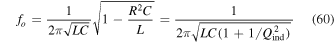
where Qind is the Q factor of the inductor.

Figure 11. Spiral inductor in parallel with C.
Download figure:
Standard image High-resolution imageWhen  ,
,  and the corresponding value of C is 5.53 pF.
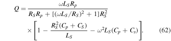
It is desired to evaluate the Q factor of the tank circuit, comprising R, C, and L, all in parallel. A simplified model of a spiral inductor is represented in O (1998) and Haobijam & Palathinkal (2014). This model is further simplified and represented in Figure 12, when one port of the inductor is grounded.

Figure 12. Simplified model of the spiral inductor.
Download figure:
Standard image High-resolution imageThe resistance Rp and the capacitance Cp are related to the modeling of the substrate whose effect is neglected. The circuit in Figure 12 is equivalent to the circuit in Figure 11 where the parallel resistance Rp is added and C is the sum of Cp and Cs . Therefore, the expression of the Q factor of Figure 12 in (61) and (62) and from Haobijam & Palathinkal (2014) can be used to evaluate the Q factor of the output tank circuit. It is found that the Q factor of the tank circuit is equal to 2.38
The value of Lo is required to be as low as possible, to reduce its size. Therefore, from (54), a low Q is preferred. Although the Q factor of the spiral inductor is already low, the Q factor of the output tank circuit can be reduced further by adjusting Rp . The values of Lo and Co derived from (54) and (56) are respectively 6.931 nH and 1.812 pF. The values of f1 and f2 derived from (57) and (58) are respectively 1.01 GHz and 1.99 GHz. The plot of S22 shows that S22 is less than −10 dB in a bandwidth of 500 MHz, which is remarkable. The value of Lo is further adjusted by simulation to 7.77 nH.
A cascode circuit is used for the output stage for a low S12 (−92 dB) and the DC base bias voltage is 868 mV, corresponding to maximum gain. The input stage is biased with a base voltage corresponding to minimum NF; this DC voltage is 615 mV. Therefore, the collector current of the input transistor corresponds to the emitter density current for minimum noise. The emitter length of the input transistor is 18 μm.
The LC load of the input stage is represented in Figure 13 whose resonant frequency is fL . The frequency fL is initially required to be lower but close to 1.4 GHz, the lower end of the frequency band of the LNA.

Figure 13. LC load of the input stage.
Download figure:
Standard image High-resolution imageThe frequency of fL is 1.370 GHz. For this value of fL , the midpoint of the descending branch of the frequency response of the tank circuit corresponds to 1.42 GHz. The corresponding values of LL and CL are derived from (63) from Arshad (2008) and are respectively 2.27 nH and 5.9 pF. A similar approach is used by Adabi & Niknejad (2007), where a frequency offset is performed between fL and the operating frequency

The approach used in this work is different and is based on (30) and (8), where CL is nil. This approach results from the inference described below. The input impedance of an amplifier with capacitive feedback can be resistive when the load is capacitive. A capacitive load can be achieved by an LC tank circuit when the operating frequency f is greater than the resonant frequency of the tuned circuit. However, it was shown that the input impedance remains resistive when the operating frequency is equal to the resonant frequency of the LC tank circuit. Therefore, a capacitive load is not required to achieve a resistive input impedance for an amplifier with capacitive feedback and operating at the resonant frequency of the tank circuit.
Equation (30) shows that the imaginary part of the input impedance is related to Cf
, Cbe and L and can still be nil when CL
is nil. The real part of the input impedance is approximated by  when the imaginary part is nil. Therefore, LL
and CL
can be determined while seeking the minimum value for S11 at 1.42 GHz by parametric simulation of S11, the parameters being LL
and CL
.
when the imaginary part is nil. Therefore, LL
and CL
can be determined while seeking the minimum value for S11 at 1.42 GHz by parametric simulation of S11, the parameters being LL
and CL
.
The proposed LNA is represented in Figure 14. The resistance RL improves the stability of the input stage but decreases the noise performance. The transistors Q2 and Q3 are the output cascode stage. The emitter length for Q2 and Q3 is 3 μm.

Figure 14. Proposed LNA.
Download figure:
Standard image High-resolution image6. Simulation Results
Simulations of noise parameters and S-parameters from 0.4 to 2.5 GHz are presented in this section. The value of S11 is less than −10 dB from 1.317 to 1.502 GHz and better than −12 dB at 1.42 GHz. The output return loss S22 is better than −10 dB from 1.1 to 1.764 GHz, as shown in Figure 15. These results indicate that the proposed output matching technique can be used for large bandwidths and that capacitive feedback impedance matching can provide relatively large bandwidths.

Figure 15. Simulation of S11 and  .
.
Download figure:
Standard image High-resolution image
Figure 16. Real and imaginary parts of the input impedance.
Download figure:
Standard image High-resolution imageThe plot of the input impedance as a function of frequency is represented in Figure 16, where the real and imaginary parts of the input impedance are respectively 49.88 Ω and −0.899 Ω at 1.42 GHz, which confirm the theoretical analysis in previous sections.
A gain of 26 dB is achieved at 1.420 GHz and a reverse isolation better than −92 dB is attained, owing to the cascode output stage, as shown in Figure 17.

Figure 17. Simulation of S21 and S12.
Download figure:
Standard image High-resolution imageThe minimum possible NF (NF ) and the NF, as shown in Figure 18, are respectively 1.788 and 2.335 dB at 1.42 GHz. The bias circuit is ideal and noiseless.

Figure 18. Simulation of NF and NF.
Download figure:
Standard image High-resolution imageThe optimal noise impedance as function of frequency is represented in Figure 19. The optimum noise resistance is close to the input resistance at the operating frequency but the optimum noise reactance is not negligible, which justifies the difference between NF and NF .
.

Figure 19. Optimal noise impedance.
Download figure:
Standard image High-resolution imageThe linearity of an amplifier is characterized by the 1 dB compression point  and the third-order intermodulation intercept point referred to the input, IIP3.
  is the power at the input corresponding to a gain decrease of 1 dB at the output and defines the upper limit of the input signal.
  and IIP3 are related by the expression: IIP3 –
  = 9.6 dB (Pajkanovic et al. 2017). The 1 dB compression point is −8.5 dBm, corresponding to an IIP3 of 1.1 dBm. The power consumption of the proposed LNA is 26 mW. The plot of the output power as a function of the input power is depicted in Figure 20.

Figure 20. 1 dB compression point.
Download figure:
Standard image High-resolution imageThe amplifier is unconditionally stable when the stability factors μ and  are greater than 1, where μ and
  are defined by (64) and (65)

where 

On the Smith chart, the stability factor μ measures the distance between the area of instability and the center of the chart resulting from the load. The stability factor  measures the same distance resulting from the signal source. For a 50 Ω source and load,
  and
and  from 100 MHz to 10 GHz, as shown in Figure 21. For low frequencies, μ and μ' are close to 1 but still greater than 1 and the LNA remains unconditionally stable. This is verified by the plot of the Rollett's stability factor K in Figure 22.

Figure 21. Stability factors μ and μ' from 100 MHz to 10 GHz.
Download figure:
Standard image High-resolution image
Figure 22. Rollett's stability factor K from 100 MHz to 10 GHz.
Download figure:
Standard image High-resolution imageThe K-factor is another measure of stability and a two-port network is unconditionally stable when the K-factor is greater than 1. However, when a network is unstable, only μ and μ'can indicate if the instability occurs at the input or the output of the network, contrary to the K-factor.
Prototyping measurements will deviate from simulation results because of parasitic resistances, capacitances, inductances, process and temperature and supply bias voltage variations. At frequencies close to 1 GHz, parasitic resistances are caused by signal tracks, while parasitic capacitances result mainly from signal tracks and bonding pads. Bonding wires create additional inductances at input and output ports. The layout of the chip starts with floor planning during which the position of power and signal bonding pads, as well as the relative positions of various functional blocks of the chip and the size and the structure of interconnection tracks are investigated and determined. Parasitics extracted from the layout tool are used to update the schematic for new simulations. The impact of process variations to performance parameters can be investigated by Monte Carlo and corners simulations whose results are also used to improve the design and the layout. The results of these simulations serve to adjust the values of some components in the schematic prior to new layouts and simulations, in an iterative process.
It is recommended to use "C4" type bonding pads from the manufacturing process, only for the validation of the concept by on-chip measurements. Such pads are intended for testing and do not require bonding wires or packaging. The parasitic inductance of a typical gold bonding wire with a diameter of 25 μm is about 1 nH mm−1. Hence, a bonding wire can be used as an inductance in the base input signal path to cancel the imaginary part of Zsopt in (42). However, the bonding wire will add a reactive component to the input impedance, degrading input impedance matching. For the proposed LNA, special attention is required for μ and μ' because their values are close to 1 for low frequencies.
A comparison with previous literature is shown in Table 2.
Table 2. Performance Comparison between Similar LNAs
| Reference | Technology | Topology | Freq | Gain | S11 | S22 | NF | Temp |
|---|---|---|---|---|---|---|---|---|
| (GHz) | (dB) | (dB) | (dB) | (dB) | ||||
| Saje & Vidmar (2017) | InGaP HBT MMIC | Common source, no feedback | 1.42 | 19.3 | ⋯ | ⋯ | 2.8 | Ambient |
| Kang et al. (2011) | 0.35 μm SiGe BiCMOS | IDCE, Cap feedback, Cascode | 0.88 | 16 | 16 | −15.3 | 1.03 | Ambient |
| Liu et al. (2018) | 28 nm FDSOI | CS, cap feedback | 2.4 | 18.3 | −20.7 | ⋯ | 2.57 | Ambient |
| Tran et al. (2011) | 130 nm RF-CMOS | CS, cap feedback | 2.4 | 25.2 | −14 | ⋯ | 3.8 | Ambient |
| Howard & Cressler (2009) | 0.12 μm SiGe | IDCE | 5 to 11 | 19.1 | ⋯ | ⋯ | 2.6 | Ambient |
| This work (simulation) | 0.130 μm SiGe HBT | CE, cap feedback | 1.42 | 26 | −12 | −12 | 2.3 | Ambient |
Download table as: ASCIITypeset image
7. The Design Methodology
The proposed design is not limited to applications in radio astronomy. Therefore, the design methodology, summarized below, can be reused for other applications:
- 1.The base DC bias voltage of the input stage is determined by simulation of NF at the operating frequency fo
. The NF NF corresponds to a constant emitter current density, Jopt.
- 2.The length of the emitter of the input transistor and the number of transistors in parallel at the input stage are set to achieve, where Zin is 50 Ω and the emitter current density is Jopt.
- 3.An arbitrary value of LL for the output LC circuit of the input stage is selected. The capacitance CL is set to resonate with LL at fo .
- 4.The optimum noise resistance Rsopt being a function of Cf through ωT and gm , as per (41), gm being determined, Cf is determined by simulation to achieve the minimum NF, corresponding to an optimum noise resistance Rsopt of 50 Ω.
- 5.The DC base bias voltage of the output stage is determined by the simulation for maximum gain.
- 6.Determine at fo , S (VSWR) and the quality factor Q of the output parallel RLC circuit. The Q factor is related to R, L and C. Calculate f1, f2, Co and Lo using Equations (57), (58), (56) and (54). L and R are selected to provide the desired bandwidth and to derive a value of Lo that can be achieved in the semiconductor process of fabrication.
- 7.The feedback capacitor Cf and the tank circuit inductor LL are fine-tuned by a parametric simulation of the NF and of S11, whose value at 1.42 GHz is desired to be minimal. The capacitor CL can be replaced by parasitic capacitances at the collector of the input transistor. The resistor RL allows adjusting S11 and improving the linearity.


8. Conclusion
This paper has shown that the input impedance of a CE bipolar junction transistor can be real when used with capacitive feedback and when the load of the transistor is capacitive. This impedance remains real when the load is an LC tank circuit operating at resonance. It was also shown that impedance matching can be achieved without affecting NF in varying the length of the emitter or in connecting several transistors in parallel. Noise matching was achieved in matching the real part of Zsopt
to the source resistance, the imaginary part causing a mismatch whose impact is small when the noise resistance Rn
is high. A high Rn
is achieved when the transistor is biased for minimum noise, the collector current corresponding to the emitter current density for minimum noise. The real part of Zsopt
was made to match the source resistance in varying Cf
, the feedback capacitor. Hence, impedance and noise matching can be achieved without inductors in the base and emitter circuits of the input transistor, which avoid using on-chip inductors whose noise performance is low. An analytical method, developed to improve the bandwidth of a single-layer microstrip patch antenna, was used for the design of the output matching network. Simulation results show an NF of 2.3 dB, a voltage gain of 26 dB, with S11 and S22 better than −10 dB at 1.42 GHz. The simulated performances of the designed LNA compare favorably with similar capacitive feedback LNAs.
in varying the length of the emitter or in connecting several transistors in parallel. Noise matching was achieved in matching the real part of Zsopt
to the source resistance, the imaginary part causing a mismatch whose impact is small when the noise resistance Rn
is high. A high Rn
is achieved when the transistor is biased for minimum noise, the collector current corresponding to the emitter current density for minimum noise. The real part of Zsopt
was made to match the source resistance in varying Cf
, the feedback capacitor. Hence, impedance and noise matching can be achieved without inductors in the base and emitter circuits of the input transistor, which avoid using on-chip inductors whose noise performance is low. An analytical method, developed to improve the bandwidth of a single-layer microstrip patch antenna, was used for the design of the output matching network. Simulation results show an NF of 2.3 dB, a voltage gain of 26 dB, with S11 and S22 better than −10 dB at 1.42 GHz. The simulated performances of the designed LNA compare favorably with similar capacitive feedback LNAs.