


Abstract
With the rapid development of on-chip optical interconnects and optical computing in the past decade, silicon-based integrated devices for monolithic and hybrid optoelectronic integration have attracted wide attention. Due to its narrow pseudo-direct gap behavior and compatibility with Si technology, epitaxial Ge-on-Si has become a significant material for optoelectronic device applications. In this paper, we describe recent research progress on heteroepitaxy of Ge flat films and self-assembled Ge quantum dots on Si. For film growth, methods of strain modification and lattice mismatch relief are summarized, while for dot growth, key process parameters and their effects on the dot density, dot morphology and dot position are reviewed. The results indicate that epitaxial Ge-on-Si materials will play a bigger role in silicon photonics.
Export citation and abstract BibTeX RIS

Content from this work may be used under the terms of the Creative Commons Attribution-NonCommercial-ShareAlike 3.0 licence. Any further distribution of this work must maintain attribution to the author(s) and the title of the work, journal citation and DOI.
1. Introduction
The first transistor was created in 1947, using germanium bulk crystals as raw materials. Germanium has a lot of advantages over silicon, among which the larger hole and electron injection velocity and mobility can provide the semiconductor devices with higher frequency operation. But due to the lack of stable germanium-based insulators, silicon-based semiconductor devices eventually replaced those based on germanium and account for over 97% of all microelectronics [1]. In the past decades, however, germanium has found new applications as a key material for the electronic–photonic integration on the silicon platform [2]. SiGe heterostructure bipolar transistors are now becoming the heart of SiGe technology; they offer higher performance and less power consumption over conventional silicon bipolar and silicon complementary metal–oxide–semiconductors (CMOS) in radio frequency communication circuits [3]. In addition to its electrical advantages, germanium has found potential applications in the area of optics because its narrower bandgap lies within the telecommunications' C band. Furthermore, despite its indirect bandgap, the direct Ge Γ-valley is only 136 meV higher than the indirect L-valley, suggesting the possibility of Ge light emission by using bandgap and strain engineering on silicon wafers [4]. Owing to its inherent compatibility with well-developed silicon CMOS processing and with III–V semiconductors, germanium has been considered as an attractive material for the active layer of integrated light emitting diodes, near-infrared and mid-infrared integrated photodetectors, middle infrared optical waveguides, virtual substrates or bottom cells of multi-junction solar cells and spintronic devices [1].
Epitaxial growth of germanium on silicon or silicon-on-insulator (SOI) substrates will result in two-dimensional (2D) planar films or zero-dimensional quantum dots (QDs), depending on different growth mechanisms. The precise growth of SiGe on a surface is complicated, determined by material parameters and growth conditions, such as the crystal structure, the surface energy of the substrate, the density of atomic steps and defects, the growth temperature, the impinging fluxes of the atoms or molecules of the growth species, the surface tension, the interface energy and the strain energy in the layers. Germanium flat layers on silicon need to minimize the surface roughness and misfit dislocations that thread to the surface as threading dislocations, which are responsible for deterioration of integrated devices. For germanium QDs, their photonic and electronic applications require precise control of the dot density, dot size, shape and even the dot site.
In this paper, we will focus on the recent progress of Ge heteroepitaxy on the silicon substrate, its optoelectronic properties and the related applications in silicon photonics. First, the material characteristics of Ge and SiGe alloys are briefly reviewed, concentrating on their crystalline structure, strain state and their electronic properties. Then, we will describe the heteroepitaxial growth technologies of germanium on the silicon platform, including the fabrication of relaxed germanium flat layers, tensile strained Ge films and Ge self-assembly quantum dots (SAQDs). The review ends with a summary concerning the possible applications and improvements in integrated optoelectronic fields.
2. Germanium: structure and properties
Germanium, similar to its group neighbor silicon, is an elemental semiconductor in group IV. The lattice constant of germanium is 0.565 79 nm, 4.18% larger than that of silicon, but it near perfectly matches that of III–V compound semiconductor GaAs. That means two facts, heteroepitaxy of germanium films on bulk silicon is challenging, and germanium can be potentially used as a buffer or a substrate for III–V compound epitaxial deposition [5].
Si and Ge are miscible to form Si1−xGex alloys which consist of any molar ratio of silicon and germanium. The lattice constant of relaxed or bulk Si1−xGex (0 < x < 1) can be obtained using an empirical equation based on the variation of Vergard's law [6]

If a Ge or Si1−xGex film is grown on top of a Si substrate, and if the film thickness is below a specific value (critical thickness), the top film will be compressively strained in the plane of the film, the lattice mismatch will meanwhile introduce a perpendicular tensile strain resulting in a tetragonal distortion to the lattice. The lattice mismatch can therefore be compensated by the biaxial strain, and the top film will be misfit free. This is the case during the early stages of film formation (pseudomorphic growth). If the film thickness exceeds the critical value, the rising strain will no longer accommodate the lattice of the substrates, then dislocation defects at the interface may form, leading to a relaxed epitaxy and the film will grow with its original lattice above the interface. The maximum thickness for coherent or pseudomorphic heteroepitaxial growth is called as the critical thickness hc, above which the misfit dislocations acting to relieve the strain in the epitaxial layer appear. The critical thickness of a heteroepitaxy system has a close relationship with the misfit (f) between the epitaxial layer and the substrate, the composition (x) of alloy Si1−xGex [7], as well as the growth temperature of heteroepitaxial films. The temperature dependence of the critical thickness of InAs and Ge was observed in experiments; the critical thickness (or called the wetting layer thickness) was found to increase with increasing substrate temperature [8]. Different mechanisms have been proposed to be responsible for the temperature dependence phenomenon, among which the modified energetic mechanism shows the entropic stabilization effect to allow a film that is energetically unstable at low temperatures to become stable at high temperatures (HTs) [9].
The interface energy and lattice mismatch between the epilayer and the substrate have a strong influence on the epitaxial growth modes. Normally there are three different models: in the case of homoepitaxial deposition or a nearly zero misfit system, the layer by layer or the Frank–van der Merwe growth mode works, and a 2D defect free flat layer will be obtained; when the interface energy is sufficient to cause island formation during deposition, the three-dimensional (3D) growth with island nucleation, or the Volmere–Weber mode occurs; the third growth mechanism, namely the layer-by-layer plus island or Stranski–Krastanov mode, is uniquely confined to systems where the island strain energy is lowered by misfit dislocations underneath the islands. Figure 1 shows the schematic diagram of three possible growth modes. During Ge or Si1−xGex growth on Si, in the early growth stage, the initial layer is coherent and grows layer-by-layer; with the increment of thickness, the epilayer is strained and drives island formation, allowing the system to relieve the strain energy [10].
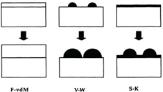
Figure 1. Schematic diagram of the three possible growth modes: Frank–van der Merwe, Volmer–Weber and Stranski–Krastanov. Reprinted with permission from [10]. Copyright 1943 by the American Physical Society.
Download figure:
Standard image High-resolution imageGe, like Si, is commonly regarded as an indirect bandgap semiconductor with the conduction band bottom at the L valley; this has made it difficult for it to be a candidate material for active components such as integrated light sources and photodetectors as compared to III–V semiconductors. Despite its indirect band alignments, Ge has a distinguishing feature different from Si, its direct bandgap at the Γ valley (EΓ1) is only 136 meV higher than the indirect bandgap (Eg), as shown in figure 2 [11]. The difference between the direct bandgap and the indirect bandgap can be further reduced by introducing tensile strain in the material. With tensile stress, both direct and indirect bandgaps will shrink, but the direct gap shrinks faster. Therefore, it is possible to utilize strain engineering to modify the band structure of germanium on silicon, and the modifications can greatly enhance the optoelectronic properties of germanium. There are several methods of strain modification. The thermal expansion coefficient difference between the germanium film and the silicon substrate will lead to about 0.2% thermally induced tensile strain after cooling down from high growth temperature (> 600 °C) to room temperature. The 0.2% thermal induced strain can decrease the difference of bandgaps from 136 to about 110 meV [12]. Another strategy to further compensate for the gap difference between EΓ1 and Eg is n-type doping to fill electrons into the L valleys up to the level of the Γ valley [13]. In recent years, an alternative approach to strained epitaxial Ge on Si has been reported by introducing tin (Sn) into the SiGe system [14]. GeSn alloys exhibit a direct band gap between 0.61 and 0.35 eV for Sn concentrations between 6 and 15%. Furthermore, GeSn alloys have exhibited higher carrier mobility than that of Ge, which makes it a promising material for optoelectronic applications.

Figure 2. Schematic band structure of bulk Ge, showing a 136 meV difference between the direct and indirect bandgaps. Reproduced with permission of [12]. Copyright 1996 World Scientific.
Download figure:
Standard image High-resolution image3. Epitaxial growth of germanium on silicon
The most important deposition techniques for the Ge-on-Si system are solid source molecular beam epitaxy (MBE) and chemical vapor deposition (CVD). The MBE system can provide ultrahigh vacuum (UHV), precisely controlled deposition rate, as well as in situ monitoring of the growing surface. In the Si/Ge epitaxy MBE system, the atomic or molecular flux of the growth species such as Si, Ge and other dopants is created by Knudsen effusion cells (for low melting point materials) or electron beam evaporators (for high melting point materials). The atomic flux can be easily switched on and off by shutters within the UHV chamber. Reflection high-energy electron diffraction (RHEED) is often well suited for use with the MBE system to characterize the surface of crystalline materials. Figure 3 shows the 2 × 1 and 7 × 7 reconstruction on 'epi-ready' surfaces of Si(100) and Si(111) substrates, respectively after the standard cleaning procedure and thermal etching procedure. Due to the small glancing angle between the incident electron beam and the substrate surface, RHEED patterns can provide the crystallographic and morphology features of the newly formed sample surface. In Si/Ge MBE growth, the germanium content of a film is dependent predominantly on the fluxes of the sources and not on the substrate temperature or the chamber pressure. The substrate temperature, on the other hand, has a significant influence on the surface migration length of adatoms, and this will result in specific surface morphology of strained or relaxed SiGe materials.
Figure 3. RHEED patterns of Si (100) (a) and Si (111) (b) surfaces, showing the 2 × 1, 7 × 7 surface reconstructions, respectively.
Download figure:
Standard image High-resolution imageThe CVD process for the SiGe system has been developed into the main equipment for mass production. The CVD techniques use gas sources such as GeH4, SiH4, Si2H6 or SiCl2H2 for pyrolysis of the precursor gases at elevated temperatures. Extremely precise control and reproducibility of the deposition rates can be achieved in most CVD methods for pseudomorphic SiGe layers. In contrast to the MBE process, the Ge content of a film in CVD epi-growth will not only be determined by flow rates of the gases, but also be affected by the substrate temperature and chamber pressure as well.
3.1. Epitaxial growth of Ge on Si with low defect density
The first attempt to realize Ge epitaxial growth on Si was made by Kasper et al [15]. They reported the short period one-dimensional Ge/Si1−xGex (0 < x < 0.15) superlattice deposition on silicon, and their experiments show that mismatch above 8 × 10⁻³ favors growth by 3D nucleation.
For heteroepitaxial films deposited beyond the critical thickness, misfit dislocations are inevitably generated at the substrate/film interface and typically propagated toward the film surface as threading dislocations. Furthermore, 3D island-like growth leads to high surface roughness, high densities of threading dislocations can significantly deteriorate optoelectronic properties of devices. For example, it will increase the leakage current of a rectifying junction and thus reduce the efficiency of photodetectors. High surface roughness, similarly, will cause difficulties in process integration.
Because of the 4.2% lattice mismatch between Ge and Si, Ge epitaxial layers on Si substrates have high threading dislocation density (TDD) and surface roughness. In order to suppress the 'island-like' growth and surface fluctuation, various methods have been proposed to realize low TDD and smooth surface. A fully relaxed thick graded SixGe1−x layer is often used as a template to match the lattice constant of the underlying layer with that of Ge. Because the surface energy of SixGe1−x is lower than that of Si, and the mismatch between SixGe1−x and Ge is smaller than that of Si and Ge, introduction of graded buffer will result in 2D pseudomorphic growth of upper layers in the Franck–van-der-Merwe growth mode. The compositional gradient of the buffer layer, the misfit dislocation nucleation temperature and the strain level in the structure will contribute to TDD and surface roughness, so optimization of the buffer step grading rate and growth temperature is indispensable [16, 17]. If an intermediate chemical mechanical polishing step is implemented, a low TDD of 2.1 × 106 cm−2 can be realized [18]. The Sb surfactant mediation technique has also been reported combining the thick graded buffer to achieve very low TDD (5.4 × 105 cm2) and the smooth surface (3.5 nm) in Ge epitaxial layers. One monolayer Sb is found to have an effect to relieve stress caused by large mismatch between Si and Ge [19]. Since the thickness of the graded buffer layer can reach the micrometer order, such a thick graded SixGe1−x layer is complex for material structure and growth control. An ultrathin buffer layer is therefore required from the manufacturing point of view. Nakatsuru et al [20] reported that using an ultrathin (on the order of 10 nm) SixGe1−x buffer layer is really an effective way to deposit pure Ge epitaxial films on Si with very low TDD and smooth surface (root mean square = 0.44 nm). Their results indicate that SixGe1−x buffer layers with two distinct interfaces are effective to absorb strain released by the Ge epitaxial layer upon relaxation and to reduce threading dislocations.
Low temperature (LT) and HT two-step growth of Ge on Si substrates is another practical method frequently reported in recent years to realize high quality Ge flat films. A two-step process means thick relaxed HT Ge layers epitaxially grown on silicon after insertion of a LT-grown Ge buffer layer [21]. In this technique, the low-temperature Ge buffer layer is able to prevent the 3D nucleation of Ge. The LT layer, also called as the Ge seed layer, is ultrathin (30–50 nm), deposited at 300–400 °C to relieve misfit stress and maintain a smooth surface by limiting the mobility of Ge adatoms at lower temperatures. The HT layer, however, is a thick relaxed film grown at 600–700 °C for faster growth rate and higher crystallization quality. Normally the two-step growth approach is combined with thermal annealing to achieve a smooth surface and low defect density. There are several thermal annealing methods reported, including cyclic thermal annealing and multiple hydrogen annealing for heteroepitaxy [22]. Kimerling's group [23] reported their results of the Ge epilayer fabricated with the two-step UHV/CVD process combined with cyclic thermal annealing. In their samples, a pure Ge seed layer as thin as 30 nm was deposited at 350 °C, then the furnace temperature was raised to 600 °C and 1 μm of HT Ge was grown on the seed layer. Finally, the wafers were cyclic annealed between a high annealing temperature (TH = 980 °C per 10 min) and a low annealing temperature (TL = 780 °C per 10 min) for ten cycles. The cyclic temperatures of TH and TL were optimized to maximize the dislocation velocity. The measured TDD was 2.3 × 107 cm−2.
Selective epitaxial growth (SEG) techniques, or called epitaxial necking techniques, have already found many applications in semiconductor heteroepitaxy and device fabrication. The techniques involve substrate patterning and epitaxial lateral overgrowth (ELO). SEG has been extensively used recently in the development of GaN devices [24]. In contrast to conventional lattice mismatched growth on planar substrates, SEG of Ge-on-Si is a kind of area dependent multi-step deposition process; it restricts the Ge epitaxial growth in small patterned regions (< 40 μm), and dislocations can glide to the edge of the mesas and annihilate [25, 26]. Small mesas on silicon are formed by etching through dielectric mask layers of SiO2 and reaching the surface of Si substrates. The dielectric SiO2 is chosen as a mask layer because the reaction byproducts of GeH4 or Ge with SiO2 are volatile GeO2, which are not stable at the Ge growth temperature (600–650 °C), resulting in the impossibility of poly-Ge nucleation on the SiO2 layer or side wall. Ge epilayers can therefore be selective grown on the patterned windows [27]. The mechanism of dislocation density reduction in the SEG process is analogous to that of bulk Si Czochralski crystal growth where the seed crystal is first necked to eliminate defects before the boule is pulled. As threading dislocations are not parallel to the growth directions, they are probably arrested by oxide sidewalls, so the SEG process can eliminate defects originated in the seed window interface. Thus in the upper part of the Ge film, especially in the ELO region, TDD will be greatly decreased. Patterned window sizes, the aspect ratio (AR) of the windows, as well as SEG growth technology have a combined contribution to the low-defect density Ge on Si. It is worth mentioning that ELO typically needs much finer patterns than regular SEG. For low defect density, the growth region is often chosen as submicron wide, and the AR is usually much larger than 1.
In the author's lab, a defect density comparison has been made by growing a Ge film on bare Si substrates and on a 70 nm-diameter Si pit with SiO2 windows; the result is shown in the transmission electron microscopy (TEM) image of figure 4 [28]. Ge grown on planar Si substrates with the typical two-step process has a threading density larger than 108 cm−2, as shown in figure 4(a). In contrast, defects including threading dislocations and stacking faults originated in the interface of the Ge film and the strained Si1−xGex seed can be rarely found in the SEG region, as shown in figure 4(b). The coalescence process will probably result in twins and stacking faults in the ELO region. Through etch-pit-density counting and TEM observation, the average of the defect density of SEG Ge films is two orders of magnitude lower than the directly grown Ge sample.

Figure 4. Defects density comparison in TEM images of Ge epitaxial grown on the bare Si substrate (a) and selectively grown on 70 nm diameter Si pits with SiO2 windows on top (b). Defects in SEG and ELO regions are indicated with white arrows and black arrows, respectively [28].
Download figure:
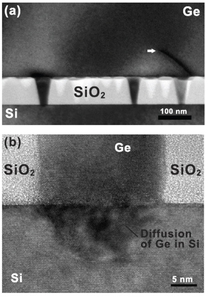
Standard image High-resolution imageSEG windows are normally fabricated with dry etched or wet etched patterned thermally grown SiO2 thin films. Substrate patterning can be performed by conventional lithography technology. But due to the relatively high cost of the lithography process and its limitations to achieve the nanoscale window size, several lithography-free methods have been proposed in recent years to realize nanoscale selective Ge growth. Li [29] reported high quality Ge SEG with nanoscale 'seed pads'. The seed pads were 7 nm wide uniform tiny regions formed by reaction of Ge adatoms with a 1.2 nm thick chemical SiO2 layer and touchdown on Si substrates. The Ge selectively grew on the seed pads rather than on SiO2, and the seeds coalesced to form the epilayer. Another lithography-free substrate pattering method uses an ultrathin free-standing porous alumina membrane (PAM) as an etching mask [28]. PAM is fabricated by a typical two-step electrochemical procedure using high-purity aluminum foil as raw material; it has uniform ordered hexagonal-aligned patterns, with controllable pore size and AR. Freestanding PAM can be used to transfer nano-patterns onto Si without introducing any contaminants. The PAM with 60 nm pore size and 300 nm thickness (AR = 1 : 5) can be used to obtain 20 nm patterns on Si by utilizing the shadow effect during the reactive ion etching process. Figure 5 shows TEM images of selective Ge films grown on 20 nm regions and coalesce to form the epitaxial layer, no defects can be observed in the windows, while rare coalescence defects exist in the ELO regions. From the defect-free growth results we can fully verify the theoretical prediction of Luryi and Suhir [30], who proposed in 1986 that if the Si substrate is patterned with tiny regions less than 20 nm, the critical thickness of Ge deposited in such small windows can be extended to infinity, which implies that Ge of arbitrary thickness can be epitaxial grown on Si with no dislocations.

Figure 5. (a) Cross-sectional TEM image of selective epitaxial Ge films grown from Si with inverted-cone-like SiO2 windows (20 nm on average at the interface). No defects of epitaxial Ge can be observed in SiO2 windows, while rare coalescence defects (white arrow) still exist. (b) High-resolution cross-sectional TEM image shows the details of the Ge/Si interface. The strain contrast below the interface indicates the diffusion of Ge in the Si substrate [28].
Download figure:
Standard image High-resolution image3.2. Tensile strained Ge films' epitaxial growth on Si
Biaxial tensile strained Ge epitaxial layers on Si have potential applications in integrated optoelectronics. Because of strain-induced band structure modification, Ge is likely to transform from the indirect bandgap to the direct bandgap semiconductor with about 1.75% biaxial tensile strain. Furthermore, tensile strain raises the light-hole band, resulting in the increment of optical gain for high injection. Tensile strain in Ge is not only beneficial for optical devices, but also good for electrical devices. Both the electron and the hole mobilities greatly increased under in-plane biaxial tensile strain.
Kimerling's group in Massachusetts Institute of Technology reported their exciting results of the first optically pumped Ge-on-Si laser operating at room temperature in 2010 [31]. The Ge epitaxial layer was fabricated with the SEG process. When the thickness of the epilayer exceeded 200 nm, the Ge fully relaxed at the growth temperature of 650 °C, but a thermally induced tensile strain of 0.24% was accumulated upon cooling to room temperature. A phosphorous doping level of 1 × 1019 cm−3, as well as biaxial tensile strain in the film allowed enhanced light emission from the direct gap of 0.76 eV. An electrically pumped germanium laser was subsequently reported by the same research group 2 years later [32]. Their results have no doubt attracted more attention on strained Ge film growth [33, 34].
However, the thermally induced tensile strain process resulting from the thermal expansion coefficient difference has some limitations. Firstly, it is difficult to precisely control the strain state during the deposition procedure. Secondly, the predicted maximal tensile strain in the Si/Ge system is only 0.3%, far below the predicted value required for direct band gap transition [35]. Aside from thermally induced strain, there are several other methods reported in recent years to achieve controllable and tunable strained Ge films. Ge growth on a large lattice-parameter substrate such as InGaAs or GeSn buffer layers may cause tensile strain in the upper films. Fang et al [36, 37] reported that up to 0.25% tunable tensile strained Ge epitaxial films had been realized using a fully relaxed Ge1−ySny (y = 0.015–0.025) layer as a buffer. As the Sn incorporation into Ge was facilitated by a quite low temperature growth step to suppress Sn surface segregation, the GeSn alloys were therefore deposited on Si at a temperature around 350–380 °C. After cyclic annealing to relieve the residual strain, the buffer layer was found to have a planar surface and lower than 106 cm−2 threading defect density. The subsequent Ge epilayer was deposited in a manner to enable built-in pseudo surfactant growth behavior. Both measurements of x-ray diffraction reciprocal space maps and Raman spectrum confirmed the strain level of the Ge epilayer. Huo [38] used relaxed step-graded InxGa1−x As layers as large lattice constant buffers to provide tensile strain; the graded InxGa1−x As layers were deposited on GaAs substrates with a relatively high In concentration of up to x = 0.40. About 2.3% in-plane biaxial tensile strained thin Ge epitaxial layers were achieved with smooth surfaces and low TDD (in the 107 cm−2 range). The strong photoluminescence (PL) of the highly tensile strained Ge layers suggested that a direct band gap semiconductor had been achieved.
3.3. Ge self-assembled QDs on Si
As the Si/Ge heteroepitaxial system has a large lattice mismatch, when the thickness of the initial layer exceeds the value of the critical thickness, Stranski–Krastanov (S–K) growth occurs and energy-quantized self-assembled islands, or called QDs, are formed on the substrates. Unlike flat Ge epitaxial layer growth, the driving force of the 3D island formation is the relief of the elastic strain accumulated in the Ge film due to the lattice-mismatch between Ge and Si. It is found that S–K growth of Ge on Si (100) is initially dislocation free [10] when the island height is below the S–K critical thickness. Furthermore, the quantum confinement effect on excitons in Si/Ge nanocrystals will allow the indirect to direct bandgap optical transition without phonon emission or absorption, offering opportunities for the development of optoelectronic devices integrated on silicon.
Ge/Si QDs exhibit a typical type-II band alignment. The large valence band offset gives rise to an effective confinement of holes within Ge islands while electrons are mostly present in the surrounding Si close to the interface [39]. The dot size, density, shape, Ge content in the dots and even the dot site can have different influences on the dot band structure, resulting in multi-modification of the photoresponse of QD-based infrared devices such as photodetectors and electroluminescent devices. Indeed, fabrication of defect free, as well as dot size, shape and site precisely controlled Ge self-assembled QDs is indispensable to develop novel devices in the telecommunication wavelength.
A conventional Stranski–Krastanov growth starts with the nucleation of 3D islands, and the surface migration phenomenon plays an important role in the 3D island evolution. Germanium 3D growth under thermal equilibrium (with high surface diffusivities or low deposition rates) and kinetically limited (in the form of low surface diffusivities or high growth fluxes) conditions will result in different island morphologies. Growth corresponding to the thermal equilibrium state shows the island size a stable Boltzmann distribution, while kinetic growth induces a coarsening process to take place: some islands continue to grow while others shrink and disappear. The uncontrolled coarsening process often leads to low island density and bimodal distribution of the island size in a wide range of growth conditions, shown in figure 6. Unimodal distribution of Ge islands can be achieved by optimizing growth parameters such as substrate temperature, deposition rate, Ge coverage, as well as annealing temperature and time [40]. Besides size distribution and island shapes, values of the Ge island dimension and island density are also key parameters for application to the actual devices. The quantum confinement effect requires the horizontal and vertical dimensions of isolated Ge islands less than its effective Bohr radius, and the lateral coupling effects between adjacent dots require Ge islands with a high areal dot density of more than 1011 cm−2. According to theoretical calculation of 3D confinement of an electron–hole pair in an infinite spherical potential, the effective Bohr radius of Ge is estimated to be 24.3 nm [41]. In order to obtain strong confinement of electrons and holes in both horizontal and vertical directions, Ge dots with the lateral size less than 10 nm and heights shorter than 5 nm are required for optoelectronic device applications. Self-assembled Ge dots based on S–K growth mode on silicon usually have a multifaceted dome shape with relatively large base dimensions and broad size distribution of 50–100 nm, short heights of 5–10 nm and a low dot density of 109–1010 cm−2. Such self-assembled dots have poor lateral carrier confinement, and the lateral coupling between dots is also weak.
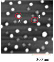
Figure 6. 2D atomic force microscopy (AFM) image of typical bi-modal Ge dots: (A) multifaceted domes and (B) square-based pyramids. Reproduced with permission from [40]. Copyright 2003, AIP Publishing LLC.
Download figure:
Standard image High-resolution imageConsiderable efforts have been devoted to control the size uniformity, density and positioning of self-assembled nanostructures in recent years. Among these methods ever reported, the Si surface covered with an ultrathin oxide layer [42] is particularly a promising candidate as a substrate for growing Ge QDs with sufficiently high density and small size. Si(111) with a 1.5 nm thick chemically oxidized SiO2 layer was used as a substrate, and Ge of an equivalent thickness of 3–13.5 nm was deposited directly on a SiO2 layer at 400–700 °C with MBE growth. Under optimized growth parameters, small (10 nm), uniform and densely packed (3.5 × 1011 cm−2) QDs were obtained. The high uniformity in the dot size and the high density of dot distribution were ascribed to the dense nucleation windows formed by reaction between Ge adatoms and ultrathin SiO2.
The growth of self-assembled QDs performed on planar substrates leads to random nucleation of dots. Thereby size control and exact placement of dots are hard to achieve. More recently, selective growth of islands in the patterned nanoscale region, or pattern guided growth, has been proposed and has attracted considerable attention. Patterned assisted QDs with precisely controlled site placement, size distribution and dot density have been realized in various nanostructures, including buried dislocation networks [43], stripe mesas [44], 2D hexagonal pits array [45] and lithography-based optical interference patterns [46]. Due to ordering of growth patterns, 2D and 3D QD arrays with perfect site periodicity and size distribution can be obtained provided that the growth parameters are optimized. Lateral and vertical coupling of QDs in ordered dot arrays will probably lead to some unexpected phenomena. Grützmacher et al [47] employed the extreme ultraviolet interference lithography (EUV-IL) technique at a wavelength of 13.5 nm to fabricate prepatterns on Si substrates. EUV-IL allowed an excellent precision of pattern control in the subnanometer regime; it also allowed for the formation of patterns with less than 30 nm periodicity. Nearly perfect three-dimensionally ordered SiGe QD crystals with small dot sizes and periods both in lateral and vertical directions had then been grown by MBE, as shown in figure 7. Temperature-dependent PL spectra showed the strong PL line centered at 746 meV at low temperatures, the PL line shifted to higher energies while increasing the temperature and the PL persisted up to room temperature. The relatively strong PL in 3D Ge QD arrays was attributed to precisely located dot cites, uniform size distribution, low defect densities, as well as excellent crystalline perfection.
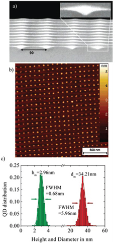
Figure 7. Images of ten period stacks of Ge islands and the Si spacer layer (10 nm) deposited on a prepatterned area. Panels (a) and (b) show cross-sectional TEM micrographs and AFM data, respectively. For dots grown on the prepatterned area, the corresponding histogram (panel (c)) illustrates the narrow size distribution in diameter and height of the Ge dots at the top surface of the 3D QD crystal. Reprinted with permission from [47]. Copyright 2007 American Chemical Society.
Download figure:
Standard image High-resolution imageWith the rapid development of on-chip optical interconnects, the efficient silicon light source is one of the most important photonic integrated devices on the Si platform. Among a lot of solutions to light emitting devices proposed lately, Ge self-assembled QDs are considered as effective candidate materials due to compatibility with CMOS technology. However, the light emission efficiency from Ge dots is still insufficient and the spectrum purity is poor. Embedding Ge self-assembled QDs into microcavities and microdisk resonators has been reported, and strong room-temperature resonant PL from microcavities [48], as well as current injected light emitting from the microdisk [49] have been observed, respectively. Figure 8 shows the schematic structure of the fabricated current-injected Si-based light emitting device. Stacks of Ge self-assembled QDs and silicon spacer layers were embedded into a Si microdisk resonator on SOI with a vertical p–i–n junction for current injection. Under forward bias, three whispering gallery mode resonant electroluminescence (EL) peaks located at 1.191, 1.241 and 1.296 μm were clearly seen at room temperature in figure 9. They are verified as transverse magnetic (TM) polarized modes with orders of TM02,27, TM03,12 and TM03,11, respectively. The room temperature EL peaks might be originated in current injected light emission of Ge QDs in the Si microdisk resonator, but the possibility that the peaks are from the defects in Ge layers is not precluded; further measurements to clarify the luminescence origin are needed. The result showed a possible route to develop a Ge QD-based integrated light source on the Si platform.

Figure 8. Cross-sectional view of the structure of the current-injected light-emitting device [49]. Reproduced with permission of The Optical Society.
Download figure:
Standard image High-resolution image
Figure 9. Electroluminescence spectra at different currents. The inset shows the red shift of the resonant peak against the injected current [49]. Reproduced with permission of The Optical Society.
Download figure:
Standard image High-resolution image
It is worth noting that the intermixing effect cannot be ignored when growing Ge dots on silicon substrates. During the deposition process, Ge will intermix with the substrate to form a layer of strained SiGe alloy. Ge islands nucleating and growing on such alloys will have a substantially different composition from the alloy layer [50]. Such stress-induced segregation consequently affects the optoelectronic properties of devices based on Ge dots.
4. Summary
In summary, we have reviewed the progress in heteroepitaxial growth of Ge on Si substrates in the past decades. The 4.2% lattice mismatch between these two materials brings great challenges to achieve epitaxial Ge flat films with high quality. Compositional graded buffer layer, LT/HT two-step and cyclic thermal annealing, SEG, etc have been proved to be valid solutions to the relief of TDD and surface roughness. Tensile strain in Ge films can tune the band structure of germanium, so band engineering by tensile strain is becoming a hot research topic. The thermally induced tensile strain plus N-type doping, buffer layer with a larger lattice parameter, and GeSn alloys are promising for efficient direct bandgap transition, making tensile strained Ge or GeSn the potential light emitting diode materials. Ge self-assembled QDs, on the other hand, benefit from the lattice mismatch. Ge SAQDs with uniform size and placement and high density are suitable not only for PL devices and IR photodetectors, but also for further studies in nanoelectronics, spintronics and for quantum computing as well.
Acknowledgments
This research was supported by the National Basic Research Program of China (973 Program, number 2013CB632104), the Natural Science Foundation of Zhejiang Province of China (number LZ12F04002) and the Research Foundation of State Key Laboratory of Modern Optical Instrumentation.