

Abstract
In this review, we report on fabrication paths, challenges, and emerging solutions to integrate group-IV epitaxial quantum dots (QDs) as active light emitters into the existing standard Si technology. Their potential as laser gain material for the use of optical intra- and inter-chip interconnects as well as possibilities to combine a single-photon-source-based quantum cryptographic means with Si technology will be discussed. We propose that the mandatory addressability of the light emitters can be achieved by a combination of organized QD growth assisted by templated self-assembly, and advanced inter-QD defect engineering to boost the optical emissivity of group-IV QDs at room-temperature. Those two main parts, the site-controlled growth and the light emission enhancement in QDs through the introduction of single defects build the main body of the review. This leads us to a roadmap for the necessary further development of this emerging field of CMOS-compatible group-IV QD light emitters for on-chip applications.
Export citation and abstract BibTeX RIS

Original content from this work may be used under the terms of the Creative Commons Attribution 3.0 licence. Any further distribution of this work must maintain attribution to the author(s) and the title of the work, journal citation and DOI.
1. Introduction
Nanostructures such as quantum dots (QDs) are promising candidates to be implemented in next generation CMOS-compatible optoelectronic and nanoelectronic devices if they can be formed in regular and uniform arrays with controlled size, electrical and optical properties for which the position of the individual structure can be precisely pre-determined. In general, semiconductor QDs [1, 2] are nanostructures with spatial dimensions well below 100 nm and, hence, they are small enough so that the motion of charge carriers inside the QDs can be confined in three spatial dimensions. Consequently, the quantum confinement of electrons and holes leads to an energy spectrum of discrete, quantized states within the QDs. Exploiting those quantum properties of nanostructures led during recent years to novel electronic and optical properties which are exploited in semiconductor devices with higher performance [3], such as QD-lasers [3–6], QD-detectors [7] QD memories [8] or QD solar cells [9, 10], and QD-based thermoelectric devices [11]. Also, new concepts such as QD-based single photon emitters, quantum-computation, -cryptography and -communication [12] were developed. Due to electronic similarities, QDs are often referred to as artificial atoms. In sharp contrast to real atoms, their energy states can be conveniently tuned by the formation process and post-growth treatment including factors such as e.g. QD size, shape, chemical composition, and the properties of their surrounding like surface passivation or choice of the matrix material. Furthermore, strain effects, but also defects within and around the QDs, post-growth annealing, and ion implantation can be used to modify QD properties. In this tutorial review, we show that introduction of single crystal defects into group-IV QDs leads to particularly strong confinement of electrons and hence greatly improved light emission properties at room temperature.
Many of the recent advancements of QD properties are based on the fabrication of bottom-up nanostructures formed on random substrate positions via self-organized growth caused by lattice mismatch [13]. In this review, we will focus on self-assembled, group-IV, Ge-on-Si epitaxial QDs, formed during the growth of thin Ge layers on crystalline Si substrates [14–17]. In the year 1990, the first dislocation-free growth of Ge and SiGe QDs on Si substrates has been reported [18, 19]. Since then, numerous studies of fundamental aspects of QD growth, the nucleation kinetics and energetics, structural, and optical properties made the SiGe QD system together with the InAs/GaAs(001) system the best explored epitaxial QD system and a prototype model for hetero-epitaxial growth. Importantly, many aspects in QD growth can be transferred to other material systems, such as III–V [16, 20–22] and other epitaxial QD systems that follow the Stranski–Krastanow [13] growth mode where QDs nucleate on an initially formed wetting layer (WL) [16].
In the following decades, intense research efforts lead to potential applications of epitaxial SiGe QDs as buried stressors to enhance carrier mobility in Si channels [23, 24], as effective phonon scattering centers to reduce thermal conductivity [11, 25], as single-hole supercurrent transistors consisting of a single QD [26] and as laser gain material for CMOS-compatible lasers [6].
The possibly most rewarding, however long-standing motivation for efficient Si-based light sources concerns the implementation of QDs as light emitters for optical on-chip interconnects [27]. These are needed for future increases in circuit clock speed, further boosting the computational power of single devices. Furthermore, chip-based optical interconnects provide the potential to drastically reduce the power consumption of computers and data centers which is a major concern taking into account that the cloud-based information systems are growing at about double the rate of general energy usage [28]. A major problem of energy consumption is not caused by the transistors themselves, but by the kilometers of copper wires that carry the electronic signals in a single chip.
Recent breakthroughs in Si-photonics include light emission from strained Ge nano-membranes [29, 30], demonstrations of a highly doped, electrically pumped Ge laser [31], group-III–V QD-lasers bonded onto Si substrates [32], group- III–V QD-lasers epitaxially grown on Ge and Si substrates [33–35], a SnGe laser grown on a Si substrate and operating cryogenic temperatures [36], and lasing from defect-engineered Ge QD light sources directly grown on crystalline Si(001) [6, 37, 38].
Figure 1 schematically depicts the layer sequences of five of the aforementioned approaches. Figures 1(a) and (b) show the layer sequence for GeSn bulk lasers ([36], figure 1(a)) and for III–V QD lasers (figure 1(b)) on Ge virtual substrates grown on Si [33]. Figures 1(c) and (d) depicts III–V QD lasers grown directly on Si, i.e. without Ge graded buffer layers. The whole thickness of the GaAs, InAs and AlGaAs buffer and cladding layer structure exceeds ∼3 μm ([34, 35], figures 1(c) and (d)). This can be avoided by using all-group-IV QDs grown on Si as a laser gain material [6] (figure 1(e)) providing an elegant and cost-efficient solution for establishing optical on-chip interconnects. Recently, we demonstrated that a group-IV QD laser [6] can be fabricated if a single extended point defect in the form of a split-[110] self-interstitial is introduced into an epitaxial Ge QD by in situ Ge ion bombardment (GIB) [37] (section 3).
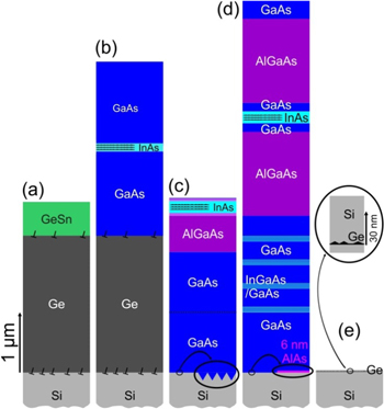
Figure 1. Comparison of possible implementations of light sources on Si. (a) Growth of bulk GeSn on top of a Ge virtual substrate grown on Si [36]. (b) Growth of multi-stacked InAs QDs on GaAs grown on a virtual Ge substrate on Si. Possible defects like dislocations at the interfaces are indicated in black [33] (c), (d) InAs QD laser structures grown directly on Si [34, 35]. (e) Ge QDs, GIB-QDs and DEQDs grown directly on Si [6, 37, 38].
Download figure:
Standard image High-resolution imageFor realistic integration of such novel QD-emitters into Si-technology devices, the QDs have to be site-controlled to ensure their large scale addressability. Besides, ordered QDs provide several more benefits as compared to their randomly nucleated counterparts: smaller size variations [22, 39–41] and, equally important, a more homogeneous chemical composition than self-assembled QDs [40, 42–44]. The three-dimensional SiGe composition within the QD directly dictates the energy band offsets and thus, influences the luminescence emission energy is at least as strong as size variations [40, 45]. Furthermore, the control of inter-QD distances opens up a number of applications. Ordered QDs with inter-QD distances larger than 1 μm [22, 46–48] can be employed as position-controlled single photon emitters [49–53], which links the field of optical data communication with large scale integration technology. However, single photon emission from CMOS-compatible QDs, possibly GIB-QDs or, in general, defect-enhanced QDs (DEQDs) where different atom species are implanted, has not been demonstrated yet. For very small inter-QD distances <100 nm [41, 54–57] wave-functions of the individual QDs can interact, forming mini-bands [58, 59], similar to molecular electronic bands. For both goals, CMOS-compatible group-IV nanostructure lasers for optical interconnects and quantum cryptography using Si-technology based single photon emitters, an integration of the nanostructure light emitters into photonic resonator structures, such as microdisks or photonic crystal cavity resonators seems to be inevitable.
The first part of this tutorial review deals with the site-control of Ge/Si-based QDs referring to the possible addressability of single GIB-QDs and DEQDs by their nucleation onto pit-patterned Si substrates. The second part deals with Ge QDs that exhibit superior optical properties upon low energy ion bombardment with Ge ions (GIB-QDs) [6] and the subsequent formation of extended point defects [37] upon annealing. Light emission of DEQDs formed upon the implantation of other atom species will be discussed. Combining these two parts seems to be a promising route towards deterministically position-controlled QDs as a laser gain material for on-chip interconnecting purposes as well as a possible route to facilitate quantum cryptographic measures directly into Si integration technology on a single platform. This would require still not existing single photon sources based on Ge/Si nanostructures. Based on these competitive perspectives, we will provide a roadmap to tackle down these goals.
2. Site-controlled QDs
2.1. Methods and sample fabrication
In this chapter, we will provide a short review of methods for obtaining ordered epitaxial QDs. In general two pre-growth fabrication steps are necessary for the fabrication of site-controlled epitaxial QDs: initial pattern formation on a mask material covering the substrate surface and subsequent pattern transfer into the substrate by various selective dry and wet etching techniques. On the ex situ cleaned, patterned substrate the epi-layers are deposited by molecular beam epitaxy (MBE) or chemical vapor deposition (CVD) techniques and QDs nucleate preferentially on well-defined locations of the patterned substrate.
Some methods based on site-selective growth e.g. growth in windows fabricated in an oxide layer on top of the substrate [60–64] are omitting one of the two steps for substrate patterning. Additionally, there exist several site-control techniques that are not based on substrate pre-structuring. One example where the ordering and QD formation is achieved only after growth involves hydrogen incorporation on masked regions of GaAs1−xNx layers [65]. There, the mask-controlled local hydrogen treatment transforms the GaAs1−xNx regions into GaAs QDs that can be utilized as efficient single photon sources [66]. Other examples of fabrication of QD-ordering without the use of substrate templates include (i) reverse epitaxy [67, 68] where ion irradiation of a crystalline surface under normal incidence and elevated temperatures leads to natural self-organization based on the interplay between surface roughening and surface-diffusion induced smoothening; (ii) ordering of QDs through vertical growth of multilayer structures [38, 69–76], (iii) strain engineering [77, 78] and (iv) by assembly of Ge micro-and nanocrystals and QDs on SiO2 via stress-induced de-wetting [79, 80].
The most successful approaches in terms of uniformity and reproducibility make use of templated self-assembly, which means that the host substrate is modified before growth. During epitaxial growth, the QD nucleation happens on predefined places of the pattern resulting in an ordered array of QDs.
For the initial pattern formation in the mask material covering the substrate different lithographic methods have been employed, such as electron-beam lithography (EBL) [22, 81–84], holographic [39, 40, 85] and extreme ultraviolet interference lithography (EUVIL) [41, 54, 56], UV-nano-imprint-lithography (UV-NIL) [46, 86], focused ion beam lithography [55, 57, 87, 88] and lithography using polystyrene nanospheres [89]. Pattern formation can be achieved using atomic force microscopy (AFM) and local oxidation [90–93] and different mask materials such as e-beam- and photo-resists, but also by using porous alumina membranes to pattern the Si substrate before growing Ge dots [94]. Certainly, all these methods have their advantages and disadvantages. Lithography using EBL- and FIB-methods are flexible with respect to pattern parameters, but time-consuming due to serial writing. On the other extreme, holographic lithography, EUVIL, and UV-NIL are methods with higher sample throughput but considerably lower flexibility for pattern adaptation. Thus, for most basic research needs, EBL is a suitable tool for pattern formation as possible substrate damage, as in the case of FIB processing, is avoided. The following discussion will, therefore, concentrate on EBL patterning.
After the pattern was defined in the mask material it has to be transferred into the substrate by dry or wet etching techniques. The former have the advantage of highly anisotropic etching rates while for the latter plasma-etching-induced defects in the substrate can be excluded2 and pits with clear defined side-facets can be obtained [49, 82, 95–97]. The influence of etching depth, pit-shape and–size on the QD growth will be discussed in section 2.2.
Before growth, the samples have to be cleaned ex situ. For the growth on Si substrates, this cleaning typically includes Caro's etch [98] (piranha etch) and RCA cleaning [99], to remove residual organic and metallic impurities at the sample surface. The native oxide is removed from the sample surface by hydrofluoric acid. Before growth, the samples are degassed in situ at about 750 °C to desorb hydrogen before the Si buffer layer growth. The degassing temperature <750 °C prevents silicon-carbide formation and changes of the pit-shape [82]. If the SiO2 is not removed before growth, it induces a large atom mobility of the Si underneath, smearing out the Si pits during the degassing step [100].
The growth of epitaxial semiconductor QDs can be divided into the two main deposition techniques, CVD [101] and MBE [102, 103]. In CVD, gaseous sources like Germane and Silane are used, hence epitaxial growth involves decomposition of the molecules and desorption of hydrogen. MBE, on the other hand, is an ultra-high vacuum technique (base pressures ∼10−10–10−12 mbar) in which the elements are deposited onto the substrate in the form of atomic and/or molecular beams. These beams usually originate from elementary pure sources that are thermally evaporated in effusion cells or by electron beam evaporators. Main advantages of MBE include the low growth rates, precise control over deposition thickness and composition, independent tunability of different growth rates and substrate temperature TG and abrupt doping profiles.
MBE growth is evidently not a method used in mass production, but it is indispensable in basic research [104] as demonstrated by a number of Nobel prizes, closely linked to MBE-grown samples: 2007 for Albert Fert and Peter Grünberg for 'The Discovery of Giant Magnetoresistance'; 2000 for Zhores Alferov and Herbert Kroemer for 'developing semiconductor heterostructures used in high-speed- and optoelectronics' and 1998 for Robert B Laughlin, Horst L Störmer and Daniel C Tsui for 'their discovery of a new form of quantum fluid with fractionally charged excitations'.
While plenty of group-IV QD related samples were grown by CVD techniques [25, 30, 60–62, 69, 105–107] we will in the following focus on MBE-growth of ordered QDs.
2.2. Parameters determining the formation of site-controlled QDs
In figure 2 we summarize the most crucial growth parameters for site-controlled Ge QD formation on pit-patterned Si(001) substrates. Those parameters are directly linked to the designed structural and optoelectronic QD properties. The nucleation position of the QDs can be shifted from in the pit center to positions at the pit rim via adjustment of the pit-depth, -diameter and -shape as well as the growth of the Si buffer layer. Furthermore, QD-distance, composition of the grown alloy, growth temperature (TG), as well as deposition-rate and -volume need to be optimized. Additional preconditions include the substrate type and orientation [108], and elimination of contaminations or crystalline defects during template fabrication.

Figure 2. Parameter-space describing the most important parameters that have to be considered for the fabrication of site-controlled, size-uniform Ge QDs enabled though pit-patterning of the Si substrate surface. Image taken from [22].
Download figure:
Standard image High-resolution imageBefore the growth of the epitaxial Ge QD layer, a Si buffer layer has to be deposited [22, 83, 85, 109]. This layer serves the following two purposes. First, the QDs are not in direct contact with the initial substrate surface, and hence electronically and optically separated from possible residual impurities at the substrate/buffer layer interface. Second, the Si buffer layer growth already decorates the initially cylinder-shaped or pyramidal shaped pits with low-energy {11n}-facets [22], driven by capillary forces [110]. The pit depth decreases while the pit-diameter and -volume increases upon Si buffer layer deposition. A likely reason for the success of forming site-controlled Ge QDs on pit-patterned Si(001) substrates is that strained Ge develops the low-energy facet {105}, 11.3° inclined to the substrate surface. This angle is close to those of {117} to {1 1 10} facets formed during Si buffer layer growth in pits [22, 83, 85, 109].
In [22] it was found that for identical pits the inter-pit-distance dpit has no significant influence on the pit-shape after Si buffer layer growth. In [22] we ascribed this finding to the lower surface mobility of Si as compared to Ge [111] caused by the larger Si–Si than Ge–Ge adatom binding energy. Notably, the independence of the Si buffer growth on dpit is in distinct contrast to the strong dependence of the QD pattern on dpit and the Ge deposition volume [22, 81, 112].
Since the contact angle of the pits after Si buffer layer and Ge WL growth critically influences the QD nucleation position, Ge growth as a function of the local substrate inclination was studied intensively [22, 57, 78, 84, 113–119]. Recently, we have demonstrated that the sidewall angle of the pit (αpit) has to be less than 30° so that QD formation in the pit is energetically favorable [84]. For αpit > 30°, substrate strain- and WL-relaxation favor QD formation at the pit-rim [84, 120, 121]. Such rim-bound QDs evolve through pre-pyramid-, pyramid-, and dome-stages [119] for which additional tweezers-like facets were found [120, 122].
Figures 3(a)–(c) depict AFM surface angle images and figures 3(d) and (e) the line scans through the pit-center pit in [109]-direction. All the facets of the wet-etched, differently sized pits were of {111}-type before growth. After Si buffer and Ge WL growth, we obtained pits with increasing sidewall inclination angles from 2° to 54.7°. In [22] we found that QD formation only occurs if αpit is larger than 5°. For lower αpit, it is energetically favorable to smooth very shallow pits. From previous work, it seems that the optimum angle αpit for nucleation of upright QDs in the center of pits is between 5° and about 18°.
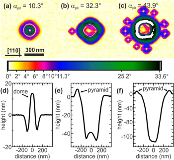
Figure 3. (a)–(c) AFM-surface angle images of the sample with originally {111}-pits with dpit = 1 μm and varying pit-diameter from 200 nm (a) to 295 nm (c) after Si buffer growth and Ge deposition of 3.8 ML at 700 °C. For shallow αpit QDs nucleate inside the pits ((a) and line scan (d)) while for large αpit QDs solely nucleate at the rim of the pits ((c) and (f)). For αpit ∼30° both, QDs inside and at the rim of the pits are found ((b) and (e)). Images modified from [22].
Download figure:
Standard image High-resolution imageFor steeper pit angles but with αpit < 30° the QDs flatten and exhibit asymmetric shape [22]. For increasing αpit from 18° to 30 °C, the nucleation position of the QDs in the pit center becomes decreasingly favorable [84] and further increase of αpit > 30° leads to QD formation around the pits (figures 3(b) and (c)).
Summarizing, perfect site-control of QDs in the pit-center requires: (i) αpit after Ge WL deposition to be between 5° and 18° and (ii) the ratio between the QD base length and the pit opening size after Ge deposition should be about 1:2 which was verified for very small QDs of 3 nm height in about 35 nm wide pits [56] and for very large coherent QDs (∼300 nm base length) grown into pits with 500 nm diameter [123].
A particular case for QD nucleation is given, if the pit-angle is steeper than 30° and the pits are touching each other, i.e. there is no space for QDs to nucleate at the rim of the pits. This was shown in [82] for patterned areas with {111}-faceted pits, wet-etched into the substrate. In this case, Ge accumulation at the very bottom of the pits is forming inverted {111}-shaped pyramids. In contrast to the III–V material system, where similar 'inverted' QDs can be used as a source of single photons [49, 95], the optical properties of 'inverted Ge pyramids' were not superior to QDs grown on a flat substrate. Such {111}-pits can, however, be used for dislocation engineering during Si–Ge hetero-epitaxy as the 60° line dislocations can be efficiently confined to the pits [96, 97].
A critical and too often neglected role for uniform QD nucleation is played by the rate of Ge deposition. Local differences in the chemical potential lead to Ge adatom migration to the pits via surface diffusion. For a high Ge growth rate, the mobile Ge on the sample surface is quickly covered by the next impinging Ge atoms. For typical Ge growth rates (∼0.05 Å s−1) it was found that Ge atoms diffuse tens of microns on the substrate and the WL surface before being captured by QDs [112, 124]. Those QDs as well as empty pits incorporate the mobile surface atoms with a capture rate that is related to the QD facet-types [112]. For QDs with fully developed faceting, such as pyramids, or, even more pronounced, domes the capture rates are much lower than for QDs with unfinished and thus not perfect crystal facets, such as pre-pyramids of transition-domes [112]. This directly hints to two points: First, there is a trend for QDs with unfinished facets to incorporate additional atoms that are used to form perfect crystal facets. Thus, this increased Ge incorporation lowers the surface energy of the system. Second, for QDs with already finished faceting, QD-stability against size-increase seems to exist.
In order to avoid satellite QDs growing between the pits, the growth rate has to be low enough to allow atom migration towards the pits and to prevent that the mobile atoms are buried by subsequently deposited atoms before reaching their energetic minimum position. When mobile atoms are trapped between the pits they contribute to WL thickening. If the WL between pits reaches a critical thickness of about 4.2 ML, satellite QDs nucleate between the pits [125]. In figure 4 this subtle balance between incorporation (red arrows) and deposition rate (green arrows) is depicted. If the incorporation rate is larger than the deposition rate, QDs nucleate only in the pits (figure 4(a)). For large pit-periods, i.e. low density of material sinks (figure 4(b)), the incorporation rate is lower than the deposition rate leading to an increase of the WL thickness and QD formation between pits. Consequently, if the number of material sinks approaches zero (i.e. very large pit-periods of several microns) even at very low growth rates QD formation between pits cannot be avoided if the amount of deposited Ge is larger than the critical WL thickness for QD formation (4.2 ML for TGe = 700 °C, [125]).

Figure 4. Scheme of a pit-patterned substrate with small and large dpit but else identical pit dimensions. The Ge incorporation and deposition rate are indicated by red and green arrows, respectively. If the incorporation rate is equal or higher than the deposition, QDs nucleate only on their favorable position. Otherwise, satellite QD nucleation on the flat areas between the pits is unavoidable, once the WL there exceeds its critical thickness of about 4.2 ML. Image taken from [22].
Download figure:
Standard image High-resolution imageIn [112, 124] the effect of long diffusion lengths for Ge ad-atoms on a Ge WL was exploited to map out the evolution of strictly ordered Ge QDs from pre-pyramids via pyramids and transition domes into domes by AFM and PL-spectroscopy. The dependence of the QD volume on the distance between the interface of the planar/patterned substrate is depicted in figure 5(a), and AFM micrographs of the respective QD shapes are shown in figures 5(b)–(g). Based on a one-dimensional diffusion model, a quantitative determination of the Ge surface diffusion constant and the rates at which Ge atoms are incorporated into the growing QDs was obtained, see figure 5(a) and [112].
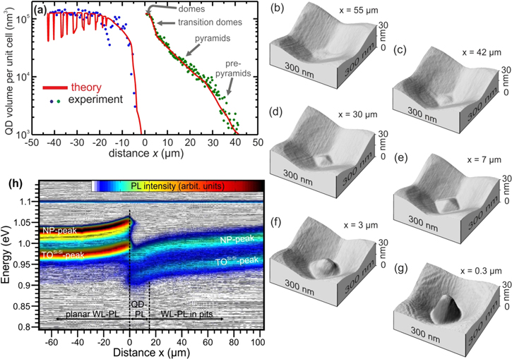
Figure 5. (a) QD volume per 300 × 300 nm2 versus distance x from the border of the fields patterned with dpit = 300 nm. Comparison between experimental results (green and blue dots) and simulations (red curves). (b)–(g) Three-dimensional AFM images taken on the field with dpit = 300 nm. (b) Pit-facet formation (c), pre-pyramids, (d) and (e) pyramids, transition domes (f), and domes (g) are observed for the different distances x (specified by the panel labels). Images (a)–(g) taken and modified from [112] (h) Contour plot of the spatially resolved PL-spectra as a function of the distance x. The shift of the PL-emission due to changing quantum confinement directly evidences the long diffusion length of Ge deposited on Si at 650 °C–700 °C. Image taken and modified from [124].
Download figure:
Standard image High-resolution imageTo quantitatively address the amount of Ge transferred at the border between planar and patterned area, we focus on the PL-signal from QDs, WL, and pit-WL. In figure 5(h) a 2D-representation of the change of the WL- and QD-related PL is shown as a function of the distance x between the planar and the patterned part of the substrate. The spectra were recorded starting from the planar part, approximately 70 μm outside the field and ending directly in the center of the patterned field at x = 100 μm [124]. The planar WL-PL undergoes a pronounced blue shift towards the border of the patterned field which is explained by increasing quantum confinement energy of the thinner WL near the border. The WL emission energy for x = −70 μm is at 1028.8 meV, which corresponds to a WL thickness of 3 ML [124], whereas the WL-emission energy at the border (at x = 0 μm) is 1056.6 meV, corresponding to a WL thickness of 2.57 ML [124]. Thus, the change in quantum confinement corresponds to a material transfer of about half a monolayer of Ge from the planar to the patterned part of the substrate over a distance of several tens of micrometers.
Upon increasing Ge deposition, steeper and larger QDs are formed on both, pit-patterned and planar substrates. Those larger QDs exhibit shapes of partially plastically relaxed superdomes or mainly elastically relaxed barns. On pit-patterned substrates, the latter evolve through cyclic growth mediated by collective shape oscillations between barn-shaped and dome-shaped QDs [123]. For optical applications such large QDs are not ideal since carrier quantum confinement and electron- and hole wavefunction overlap is diminished by the extended QD dimension. Additionally, dislocations in ordered QDs [126] lead to strong quenching of the QD related PL [81], similar to the case of randomly nucleated QDs [107]. Consequently, we will focus on the optical properties of smaller site-controlled QDs, pyramids and domes.
2.3. Optical properties of ordered Ge on Si QDs
The main advantages of site-controlled QDs over randomly nucleated ones are their inherent addressability and enhanced size- and composition uniformity. In this section, we will discuss how these features influence the QD-PL as well as parameters that are detrimental for the PL from ordered SiGe QDs.
This will guide us to the exciting perspectives of combining GIB-QDs and site-control by templated self-assembly. In [40, 127] it was shown that for randomly nucleated SiGe/Si(001) QDs (figure 6(b)), a significantly stronger blue-shift of the QD-related PL emission peaks is observed as a function of the excitation intensity (Pexc) when compared to site-controlled QDs (figure 6(a)). These PL shifts are plotted in figure 6(c). The PL emission shifts by more than 90 meV when increasing Pexc from ∼30 mW cm−2 to 245 W cm−2 in the case of the QDs on the planar substrate (figure 6(c)), whereas it virtually does not shift with Pexc for ordered QDs. In the samples investigated, we observe for domes on a planar sample (94% of all QDs, height: 20.1 ± 0.1 nm) a similar size distribution as the ones on a patterned sample. Thus, it can be safely expected that domes contribute most to the QD PL spectra. In the light of a similar QD size distribution of QDs grown on patterned and planar substrates, this different PL behavior was attributed to the much larger inhomogeneity of the Ge distribution in QDs on planar substrates [40]. Three-dimensional band-structure calculations revealed that Ge-rich inclusions of approximately 5 nm diameter at the apex of the QDs can account for the observed differences in the PL spectra. The existence of such inclusions can be regarded as a truly zero-dimensional QD within the host dot [40]. This finding is in agreement with recent nano-tomography experiments [43].
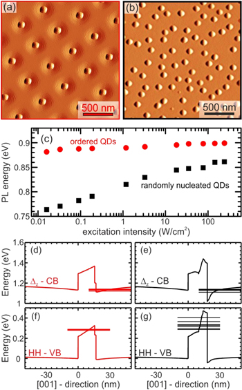
Figure 6. AFM images measured on uncapped samples (6 ML of Ge at TGe = 690 °C) grown on (a) e-beam patterned Si(001) (dpit = 400 nm) and (b) on planar Si(001). (c) Influence of Pexc on the QD-PL emission energy for ordered (red disks) and randomly nucleated QDs (black squares). (d)–(g) Calculated energy level scheme for QDs grown on pit-patterned Si(001) substrates without regions of Ge enrichment (d), (f) and QDs grown on planar Si(001)substrates containing Ge-rich regions (c), (e) as described in the text. The stronger Ge composition gradient of QDs grown on planar substrates induces a confining potential at the QD apex. The strong shift of the QD signal on planar substrates at moderate Pexc as observed in (c) is explained by the decreased density of states (indicated by the horizontal lines in (g)) in this confining potential. Images modified from [40].
Download figure:
Standard image High-resolution imageFigures 7(a)–(d) presents perfectly site-controlled QDs for dpit varying from 425 nm (figure 7(a)) to 3.4 μm (figure 7(d)). These fields were located on one and the same sample, grown in the same MBE-growth run: 3 ML of Ge were grown at TGe = 700 °C and at a growth rate of 0.03 Å s−1. Figure 7(e) presents PL-spectra containing emission contributions from QDs, the WL between QDs and Si bulk. With increasing sample temperature during PL investigations, thermal quenching of the WL-related PL signal is concomitant with a transition of carriers into the QDs. A schematic illustration of the related carrier diffusion paths is shown in the upper inset of figure 7(e). This carrier transfer is associated with an activation barrier EA2 of about 25 meV induced by a thinner WL around the pits in the vicinity of the QDs. Since almost all generated holes diffuse into the WL quantum well, they become trapped because the activation barrier prevents diffusion into the QDs. Thus, for very low temperatures efficient PL emission from the QDs is unlikely and PL spectroscopy on single epitaxial Ge QDs on Si substrates should be conducted at elevated temperatures. Figure 7(e) depicts spectra recorded at a sample temperature of 40 K. In contrast to the 10K-PL spectra (see [128]), where QD signals are barely detectable, some of the holes trapped in the WL can now overcome EA2 and diffuse into the QD. Simultaneously, the integrated PL signal decreases because of the low exciton binding energy EA1 and phonon-induced thermal PL-quenching. Overall, the relative contribution of carrier recombination in the QDs increases [128].
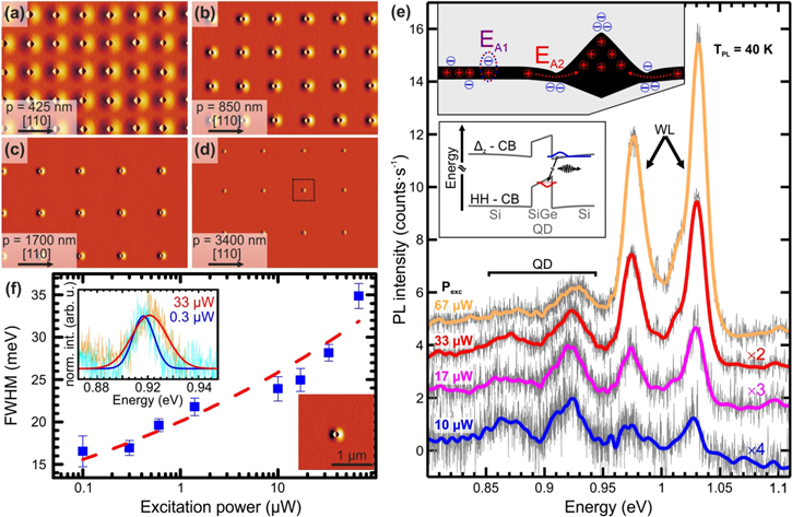
Figure 7. (a)–(d) Site-controlled QDs with variations of dpit, increasing from (a) 425 nm to (d) 3.4 μm. No secondary QDs between the pits are observed. (e) Pexc-dependent PL spectra from individual Ge QDs for TPL = 40 K. The spectra are vertically shifted. The thick curves present smoothened spectra as guides for the eye. The upper inset schematically depicts a Ge QD in a pit (black) in a surrounding Si matrix (gray). Electrons and holes are depicted as '−' and '+', respectively. Experimentally determined activation barriers EA1 and EA2 are indicated. The lower inset shows the type-II band alignment of a SiGe QD, based on self-consistent calculations. (f) FWHM of the NP-QD-peak as a function of Pexc. With decreasing Pexc from 67 to 0.1 μW, the FWHM decreases by almost 20 meV. The red-dashed line presents a phenomenological power law fit using a Gaussian function. The upper inset shows the PL-QD NP peak with the corresponding Gaussian fits for Pexc = 33 and 0.3 μW. The lower inset in presents a zoom-in of a pyramid in a field with dpit = 3.4 μm. Image modified from [128].
Download figure:
Standard image High-resolution imageIn order to minimize line broadening of the QD related PL peaks, the PL spectra of individual QDs at extremely low excitation powers between 0.1 μW < Pexc < 1.4 μW were investigated. When decreasing Pexc from about 30 to 0.1 μW we observed that the line-width of the QD-related NP-peak at 920 meV decreases to a full-width-at-half-maximum of about 16 meV, following the empirical power law  with A = 0.02006 and m = 0.11025.
These widths are significantly sharper than PL-lines from any SiGe QD ensembles published till then [54, 129]. This spectral linewidth is comparable to the ones of individual Si nanocrystals at 70 K for particles with functionalized ligands [130]. However, they are still broader than the ones observed from top-down fabricated Si QDs [131–133] and Si nanocrystals encapsulated in an oxide matrix (∼200 μeV) [130], and substantially broader than those of QDs made from CdSe (∼1.6 μeV) [134], CuCl (∼1 μeV) [135], InGaAs (∼2 μeV) [136] and ordered InAs QDs (∼500 μeV) [47], even though we employed comparable excitation power densities in [128] as in the last case.
In [128], several mechanisms were discussed that contribute to the relatively broad Ge QD-PL signals even at low Pexc. The indirect bandgap and the type-II band alignment in SiGe QDs lead to carrier lifetimes in the μs range [137, 138] that are substantially longer than, e.g., in type-I InAs QDs. Thus, even at our lowest Pexc, which is within the limits of experimental feasibility, filling effects are expected to be important [128]. Such a state filling becomes in particular important for site-controlled Ge QDs, because their rather homogeneous composition [43] causes spreading of the hole-wave-functions over most of the QD [40].
In addition, the strain distribution leads to a splitting of the six-fold degenerate conduction band (CB) of the Si matrix near the apex and the four base corners of pyramids, where the electrons are located [40, 45] adding to the complex and dense system of energy levels [139]. Another major contribution to line broadening in long-time averaged spectra comes from spectral diffusion which is caused by charge fluctuations in the vicinity of the QDs [140, 141]. Such fluctuations can, for instance, be associated with growth defects, e.g. in the low-temperature Si cap layer. Moreover, thermally induced charge fluctuations of the weakly bound electrons of our type-II excitons (inset in figure 7(e)) would lead to differently charged excitonic complexes [142]. Their energy shifts with respect to the neutral exciton level were predicted to be enhanced in type-II heterostructures [143]. Since the SiGe/Si heterosystem is indirect both in real and k-space, phonon broadening at TPL is another expected contribution to the observed line width. In [130] it was demonstrated that the mechanical coupling of a nanocrystal to its matrix largely influences the luminescence linewidth due to exciton–phonon interaction.
Thus, two strategies appear feasible to further reduce the linewidths of SiGe QDs for CMOS-based single photon emission applications. Firstly, lower growth temperature, TG could suppress interdiffusion and should thus allow smaller QDs with well-separated hole-confinement levels. It would also sharpen the interface between Ge QD and Si matrix and might, therefore, reduce exciton–phonon interaction. Secondly, locating a single QD in a photonic crystal cavity [144] will lead to reduced radiative lifetimes due to the Purcell effect, which would also reduce level filling effects. Under these conditions, time-resolved experiments should allow us to separate the aforementioned transition mechanism and to gain access to the intrinsic linewidths of individual transitions.
Both of the aforementioned strategies will also need to be applied to the recently developed GIB-QDs that will be discussed in the following. In these QDs defect-based electron states that are similar to color centers in diamond, contribute to the greatly enhanced PL intensities even at room temperature, and might, therefore, be well suited for Si-based single photon sources.
3. Defect engineering of epitaxial Ge QDs on Si
For over a quarter of a century, the fabrication of self-assembled SiGe QDs was a concern of tremendous research effort. However, the optical properties of dislocation-free epitaxial SiGe and Ge QDs, grown on Si substrates, never matched the expectations as the efficiency of their light emission is limited by three main factors. (i) Both, Si and Ge are indirect semiconductors. This implies that the difference of the momenta of electrons and holes has to be assisted by scattering or three-particle interactions via phonons, making radiative transitions improbable with quantum efficiencies of bulk materials being around 10−6. (ii) The band offsets of Ge on Si and Si1−xGex heterointerfaces are for a wide range of compositions x of type-II, i.e. only holes are confined efficiently in the QDs, whereas electrons are only weakly bound (typically ∼60 meV) by strain fields in the Si matrix around the QDs. This confinement can be ∼100 meV, but only for large QDs with base widths larger than 100 nm [40, 45, 145]. Such large QDs, on the other hand, provide almost no hole-confinement in all three-dimensions. In any way, an activation barrier of ∼100 meV for electrons is far too low for efficient room-temperature (RT) applications as electrons can escape from this confining potential already well below RT. In Ge/Si QDs, electrons and holes are not located spatially at the same positions leading to a weak wavefunction overlap and thus small matrix elements for radiative transitions. Efficient electron confinement through band-offset engineering has not yet been demonstrated (iii) Due to the relatively low lattice mismatch between Ge and Si of only about 4.2%, self-organized QDs such as domes and pyramids tend to be too large for the efficient confinement of holes in all three dimensions. While the height of domes and pyramids is typically between 5 and 30 nm, base widths are typically 50–200 nm and, thus, too large for lateral hole confinement.
In recent publications, we have provided a way to address all three of the aforementioned problems of Ge-on-Si QD light emitters [6, 37, 38]. Creating single isolated point defects within a QD allows for strong electron confinement within the QD where the holes are also confined. Due to the extreme localization of the electrons at the defect site, their k-vector is spread in momentum space, as described by Heisenberg's uncertainty principle. In this way, the Γ-point contributions of the electronic wave functions lead to optically direct and, thus, more efficient radiative transitions. Furthermore, we embed the defects in self-assembled QDs called hut clusters [14, 19, 146] that are small enough to induce strong hole-confinement.
3.1. Fabrication procedure of GIB-QDs and DEQDs
In the following, we will describe the fabrication procedure of ion bombarded Ge QDs, focusing on Ge ion implantation and emphasizing the crucial parameters that have to be taken into account to optimize the yield of radiative recombination.
We deposit crystalline Ge and SiGe QDs on Si (or silicon-on-insulator, SOI) substrates using a solid source SIVA45 MBE system from Riber. We want to stress, however, that even though in [6, 37, 38] the samples were grown by MBE in combination with in situ low energy GIB, all fabrication steps can in principle be performed with fabrication methods that are compatible with Si integration technology. In a large part of the literature about Ge-on-Si QDs (see e.g. [25, 30, 60–62, 69, 105–107]), the samples were grown by CVD and also ion-implantation and annealing are standard procedures in Si technology.
The QDs evolve in the strain-driven Stranski–Krastanow growth mode [13] on a Ge WL, once an overcritical thickness of Ge (∼4 monolayers, ML) is exceeded [16, 125]. Strain-driven plastic relaxation of the QDs does not occur for the amount of deposited Ge generally used in this work, which is typically ∼6 ML. This is important since the introduction of, e.g. 60° line dislocations in the Ge QDs due to elastic relaxation [126, 147] would quench the QD PL almost completely [81, 107]. Due to the relatively low Ge TG of 500 °C used in [6, 37, 38], the height of the Ge-rich and hut-shaped QDs is only about 2–3 nm, and the QD-density can be conveniently tuned by varying the Ge coverage [6]. GIB-QDs and DEQDs differ from conventional, epitaxial Ge-on-Si QDs by ion bombardment. For this purpose, positively charged ions are accelerated towards the sample. For GIB-QDs, low-energy Ge-ions (≤3 keV) are employed. A Ge ion undergoes collisions with Ge atoms in the QD causing a displacement cascade since the ion is rather heavy and its energy (≤3 keV) much larger than the about 14 eV displacement energy of crystalline Ge. The displaced Ge atoms in the QD, called recoil atoms, still have enough energy to displace further atoms, leading to a collision cascade of ellipsoidal shape. Importantly, the cascade of a single Ge-ion (≤3 keV) produces a single, few nm wide amorphous zone. According to TRIM simulations [148], the energy that is dissipated by the Ge ion itself through ionization, vacancy formation and the creation of phonons ranges from 14.5% to 11.5% for an acceleration voltage VGIB between 0.3 and 3 kV. The rest of the energy dissipates through the recoil atoms. Thereby, phonon formation and atom ionization in the QD due to the recoil atoms account for the main energy loss mechanisms during the GIB-process with approximately 60% and 20%, respectively [148].
The values of VGIB and the ion dose have to be chosen carefully with respect to the QD height since VGIB directly determines the penetration depth and the amount of amorphization in the sample. For ion energies smaller than 3 keV the ion becomes stopped within the height of the QD. For the thermal stability of the GIB-QDs, it is essential that GIB leads to a situation where one extra Ge atom (N + 1 atoms) is present in the volume of a QD for which N atoms would make a perfect crystal. Therefore, if VGIB is chosen too high, the ion penetrates the QD and stops only in the Si substrate where it does not contribute to the PL enhancement associated with the GIB-process [37].
Already during Ge-deposition and ramp-down to TG of the Si capping layer, partial recrystallization of the amorphized zone takes place via solid-phase epitaxial regrowth (SPER) [149, 150], in which amorphized Ge is recrystallized if the sample temperature is above about half of the melting temperature of the crystal [149, 151]. The driving force for the recrystallization process is the lower energy configuration of crystalline as compared to amorphous material, mainly due to the lack of dangling bonds (DBs) and bond-angle-distortions [149–151]. The surface diffusion-driven recrystallization starts from the surface of the crystalline parts of the QD that were not amorphized during GIB. This immediately explains the importance of choosing a not too high ion dose, i.e. not to amorphise the QD completely. For the GIB-QD fabrication presented in [6, 37], we used a dose of about 104 ions per μm2, i.e. only one to two ions hit a QD leaving enough crystalline regions from which recrystallization can commence. Full recrystallization of the partly amorphized QD is, however, inhibited by the aforementioned presence of one or two extra Ge atoms in the otherwise perfect crystal lattice. If enough thermal budget is available, e.g. through post-growth annealing or a high-enough TG of the Si capping layer, a minimum energy configuration for the bond arrangement of a QD supersaturated with an extra atom can be obtained. In [37] we found by Monte Carlo and density functional theory calculations used to crystallize amorphous Ge, containing one excess in a perfect crystal of the same volume that the system reaches an energetic minimum configuration of a split-[110] self-interstitial with concomitant displacement of the surrounding ∼40 Ge atoms, depicted in figure 8(b). The core atoms of the split-[110] interstitial are shown in black while the surrounding displaced Ge atoms appear gray. In [−110]-direction, an undisturbed Ge crystal lattice would be seen as hexagonal lattice where atoms, located in different lattice planes in [−110]-direction would not be visible.

Figure 8. (a) Scheme of a split-[110] self-interstitial with surrounding lattice deformation in a QD upon annealing or overgrowth with Si at high TG (b) ground state defect structure that results after crystallization of an amorphous state containing one extra Ge atom. The core atoms of the split-[110] interstitial are shown in black but the positions of four surrounding atoms are significantly shifted. The color coding represents the electronic orbital electron density cross-sections in the plane containing the split interstitial indicating strong electron localization at the defect site. (c) Proposed energy level diagram in the [001] growth direction. The full red oval depicts localized Γ-point electron states at the defect site. The green and blue arrows show GIB-QD PL emission of longer and shorter wavelength and the hole states in the GIB-QD are indicated by the green-blue-shaded area. Image modified from [37].
Download figure:
Standard image High-resolution imageAfter SPER, on top of the recrystallized Ge QD surface, a crystalline Si capping layer can be grown. Avoiding non-radiative recombination centers in the Si matrix is essential with respect to the optical or optoelectronic properties and the application-potential of the QDs. In [37] we found, that there exists an optimum TG-window around 475 °C, for which the PL yield of GIB-QDs at room temperature is maximized. If the capping layer growth temperature (TCAP) is too low (<400 °C), the recrystallization process of the GIB-QD surface via SPER is disturbed, leading to imperfect overgrowth and the formation of non-radiative recombination centers in the Si capping layer. On the other hand, if TCAP is too high (>600 °C) the defect structure can migrate out of the QD by overcoming an activation energy of about 3.2 eV [37].
In [37] we have demonstrated that post-growth thermal annealing at a temperature between 500 °C and 600 °C improves the RT PL properties of GIB-QD. In this case, the minimum energy configuration of a point defect with a surrounding distorted lattice can be reached, and unwanted non-radiative recombination centers that might be introduced in the Si substrate during the GIB process can be healed out. Annealing at higher temperatures (>600 °C) leads to quenching of the GIB-QD PL at RT, caused again by migration of the defect out of the QD [37]. This activation energy for migration of the defect was found to be ∼3.2 eV, which is in agreement with the activation energy for diffusion found for extended defects in Ge in [152].
Post-growth hydrogen passivation can further enhance the RT PL properties of GIB-QDs [37]. Weber et al have shown [153–156] that DBs in Ge exhibit different electronic properties as compared to DBs in Si. In Ge, the DBs create states below the VB edge that are negatively charged. Thus, interstitial hydrogen cannot efficiently passivate DB defects and electrons will not be localized at DB sites [153–156]. Therefore, optically active GIB-defects are not negatively affected by hydrogen passivation. In contrast, if the H-passivation properties are chosen correctly [37, 157], the PL yield of GIB-QDs can be increased upon H-implantation since residual crystalline defects induced by GIB in the Si substrate can be cured by H passivation. This reduces the number of non-radiative recombination channels in the GIB-QD-Si matrix system and therefore increases the PL yield from GIB-QDs.
3.2. Optical properties of GIB-QDs
Figure 8(a) schematically depicts a GIB-QD (gray), embedded in a crystalline Si matrix (tan color) containing a split-[110] self-interstitial (red color) with surrounding lattice deformation (dark gray color). At this interstitial site, the electrons are highly localized (see color map in figure 8(b)), creating states well below the CB edge of crystalline Ge [37]. Due to the strong spatial confinement, the electrons exhibit wave-function contributions at the Γ-point, as displayed by red color in the electronic orbital iso-surface cross-sections presented in figure 8(b). Figure 8(c) presents a band alignment scheme that describes possible optical recombination paths in GIB-QDs. Upon optical excitation, electrons diffuse to local energy minima in the CB, introduced by the strain fields around the QDs (open red circles in figure 8(c)). From there they can tunnel through a barrier caused by ∼1 nm of recrystallized Ge to the localized states below the CB gap introduced by the GIB-process (red arrow in figure 8(c)). Hence, electrons can directly recombine with holes confined in still crystalline regions of the QD.
Excitation of an ensemble of GIB-QDs with different sizes, the filling of the different defect induced levels and the filling of the first excited hole states at higher excitation power lead to the observed broad range of transition wavelengths in the GIB-QD PL, ranging from 1250 to ∼1650 nm [6, 38]. The energy level scheme [37] presented in figure 8(c) is consistent with the observed emission wavelength of GIB-QDs. It becomes clear that the high activation energies for thermal quenching of the GIB-QD PL of about 350 meV are consistent with the escape of holes from the confining QD potential. Importantly, this high activation energy prevents quenching of the GIB-QD related PL intensity in a temperature window from 10 K to above RT. In [6], we observed that with increasing Pexc, the integrated PL intensity (IPL) of the GIB-QDs increases with a power coefficient of m = 1 according to  This, in combination with the short observed carrier lifetimes of about 1 ns, and the efficient PL from GIB-QDs at RT and above are indications for optically direct electron–hole recombination in real and reciprocal space caused by the presence of the GIB-induced defect site in this epitaxial system [6, 37].
Finally, we want to stress that having both, the GIB-induced defect and a QD are necessary pre-requisites for obtaining high PL yields at RT and above. In contrast to PL emission from GIB-QDs, the PL signal from quantum wells (QW) that underwent the same GIB-treatment as the QDs is almost completely suppressed at RT, as can be seen in figure 9.
Figure 9. RT-PL signals of GIB-QDs (gray) and two different GIB quantum wells (QWs) (green and red). Only the GIB QDs show strong PL enhancement. Inserts: Schematic views of GIB-QDs (right) versus a GIB-QW (lower left) and a GIB-bulk sample. Holes (blue H) are confined in the GIB-QDs and thus overlap strongly with electrons trapped at defect sites (red dots). In contrast, holes in a GIB-QW or in bulk Ge can diffuse away from the two point defects (blue arrow), thus reducing the electron-hole wavefunction overlap. Image taken from [37].
Download figure:
Standard image High-resolution imageWhile the holes are efficiently trapped in the GIB-QDs, in the GIB-QW samples and also in Ge bulk samples that underwent GIB-treatment, the holes can diffuse away from the extended split-[110] self-interstitial into regions without crystal distortions between two such defects. This is schematically depicted in figure 9 by the blue arrows and the letter 'H' in the inset. The resulting charge carrier separation reduces the overlap of the electron and hole wave function and thus the transition matrix element for optical transitions. Therefore, QDs are a necessary precondition for direct optical transitions in Si/Ge heterostructures treated by GIB [6, 37] or implantation of other isolated ions (DEQDs). In contrast, enhanced PL yields can neither be observed in GIB treated quantum well structures (figure 9), nor in bulk Ge, where the split-[110]-self-interstitial is known for almost twenty years [158–161].
In [6] we have grown a single layer of GIB-QDs on a SOI substrate and fabricated a microdisk resonator with a diameter of about 1.8 μm (scheme in the inset of figure 10). The emission wavelength (λPL) of the GIB-QDs is in the near infrared telecommunication O-band around 1330 nm. Upon increased optical excitation, the PL response at 10 K from the GIB-QDs in the microdisk increases super-linearly, showing a clear threshold behavior, as well as linewidth narrowing of the emission modes above a threshold. These are two clear indicators for lasing from such structures. On a double logarithmic plot of the Integrated PL intensity (IPL) versus the optical excitation power Pexc the curve shows a characteristic S-shaped behavior, typical for light amplification by stimulated emission of radiation [6].
Figure 10. RT mode-PL-spectrum (gray—upper and right axis) from GIB-QDs in a microdisk (TPL = 300 K) and power-dependence of the integrated intensity of cavity mode TE(12, 1) on a double logarithmic scale (TPL = 300 K). The inset schematically depicts a microdisk resonator containing GIB-QDs (red) and the whispering gallery mode running around the circumference of the disk (yellow).
Download figure:
Standard image High-resolution imageAt RT, this S-shape of IPL over Pexc is still present, however, less pronounced, as can be seen in figure 10. At the threshold, IPL increases super-linearly with Pexc and eventually saturates at high Pexc > 1 mW to a value of m = 1  The gray curve in figure 10 depicts a PL emission spectrum from a microdisk recorded at TPL = 300 K. The pronounced maximum of the PL at about 1330 nm is the emission from the whispering gallery cavity mode TE(12, 1), running around the circumference of the microdisk.
This finding implies that strong RT light emission and even lasing is feasible using GIB-QDs as gain material. Moreover, this monolithic solution might be the long-awaited missing piece of Si photonics marking a major step towards optoelectronics integration on Si for high-performance optical communication and computing applications.
3.3. Further improvement of the optical properties of GIB-QDs and DEQDs
At this point, we want to stress that until now, microdisk resonators containing only single layers of GIB-QDs were fabricated. One straightforward way to further increase the PL yield of GIB-QDs and epitaxial QDs, in general, is by increasing their sheet density through vertical stacking. In such a way, the density of emission centers increases linearly with the number of layers. Over the last decades of QD-related research, a lot of research effort has been devoted to the growth of multilayer structures that are separated by a matrix material that typically has a similar composition as the host substrate [38, 69–76]. Concerning GIB-QDs as compared to fully crystalline QDs, the growth of stacked layers turns out to be more difficult, simply due to the intentionally induced amorphous zone in the GIB-QDs that has to be overgrown consistently by crystalline Si for every QD layer. In [38] we have shown that if only a single GIB-QD cannot be overgrown in a crystalline way, this will lead to a full breakdown of the growth in the following layers above the GIB-QD, as can be seen in figure 11(b). This can be avoided if the growth temperature of the Si spacer layer is chosen to be about 500 °C, the optimum temperature for the overgrowth of GIB-QDs [37]. Figure 11(a) shows a high-angle annular dark field transmission electron microscopy image of an eleven-fold stack of GIB-QDs. For this successful stacking of GIB-QDs, the PL yield was found to increase by a factor of 7 (blue spectrum in figure 11(c)) as compared to the single layer samples (gray spectrum in figure 11(c)) for which lasing was demonstrated [6]. For the sample containing the large defect induced by non-successful solid phase epitaxial regrowth during the growth of the Si spacer layer, no PL was observed at RT, as can be seen in figure 11(c) by the red spectrum [38].
Figure 11. (a) HAADF STEM images of an 11-fold stack of GIB-QDs (light gray) separated by 15 nm thick Si spacer layers grown at 500 °C–600 °C (sample A). (b) HAADF-STEM image of a 10-fold multi-stack of GIB-QDs where the 12 nm thick Si spacer layers were deposited at 350 °C–500 °C (sample B). (c) RT PL spectra obtained from a single layer of GIB-QDs (gray) and from an 11-fold stack (blue) for which TSi was 500 °C–600 °C. For the multi-stack sample for which the growth parameters were not optimized (TSi = 350 °C–500 °C), no PL signal was recorded (red). Image adapted from [38].
Download figure:
Standard image High-resolution imageThus, PL enhancement from GIB-QD multilayers can be achieved, if the growth conditions of the Si spacer layer are chosen appropriately. For the formation of lasing devices using GIB-QD multilayers as gain material, the main challenge will be to achieve photonic structures with smooth sidewalls after the etching process as enhanced sidewall roughness caused by different etching rates of Si and Ge will lead to a decrease in the quality factors of the devices.
3.4. Site-control of GIB-QDs and DEQDs: feasibility and applications
Up to now, only GIB-QDs and DEQDs in the form of randomly nucleated QDs have been investigated. The two main applications will employ GIB-QDs (i) as gain material for CMOS-compatible group-IV nanostructure lasers in optical interconnects and (ii) for quantum cryptography using single photon emitters based on Si technology. For both goals, two main conditions will have to be fulfilled. (i) For any kind of large scale integration, addressability of the QDs is a must, and (ii) the QDs will have to be embedded into optical resonators if possible located at positions where the cavity modes exhibit maxima. Both conditions can be fulfilled by the growth of QDs at predefined positions, e.g. by the growth of ordered QDs via templated self-assembly. The dominant material classes [162] for state-of-the-art solid-state single photon sources are (i) defects in bulk 3D crystals, such as nitrogen-vacancy [163] and Ge vacancy centers [164] in diamond, silicon carbide [165, 166], yttrium aluminum garnet [167] and zinc oxide [168]; (ii) self-assembled III-V QDs, such as InAs QDs grown on GaAs [11]; (iii) emitters from defects in two-dimensional hosts such as WSe2 and MoSe2 [169]; and (iv) localized oxygen-related defects in single-walled carbon nanotubes [170]. By using GIB-QDs and DEQDs we aim at merging topic (i) and (ii) by using defects within group-IV QDs.
For III–V QDs, single, self-assembled and randomly nucleated QD are chosen as single photon emitters. Strategies for the fabrication of large numbers of identical QD-cavity emitter units which are necessary to implement mass-produced integrated cryptography are missing thus far. This is a major advantage of the Si–Ge QD system (see chapter 2) over III–V QDs, for which spatial matching between cavity and QD can only be achieved with extremely low yield or under degraded QD performance. The possibility of CMOS-compatible parallel processing of cavity-enhanced single-QD emitters might ultimately tip the scale in the transition from purely academic single photon sources to mass-produced, integrated optoelectronic systems.
Figure 12(a) depicts a perspective view of an AFM image of ordered QDs (red color) grown on a substrate with regular arrays of pits (black color) with different pitch, ranging from 325 nm to 3.4 μm. In the Ge/Si system, growth of ordered and uniform QDs with different pit-spacing is possible even on one-and-the-same sample if the growth and substrate patterning parameters are carefully adjusted (chapter 2). Choosing a QD system with high inter-QD spacing provides access to a single QD as a possible emitter of single photons, as schematically indicated in figure 12(a), and to address several emitters in a controllable fashion. Furthermore, in combination with photonic resonators, the QDs can be intentionally placed into the maxima of the cavity modes, as shown in figure 12(b) and reported in [144, 171].

Figure 12. (a) AFM image of ordered Ge QDs grown on a pit-patterned Si(001) substrate with inter-pit distances ranging from ∼400 nm to ∼4 μm. Such widely spaced QDs are promising candidates for single photon emitters in this group-IV system, as schematically indicated. (b) L-3 Photonic crystal cavity containing a single Ge QD. Image (b) taken from [143].
Download figure:
Standard image High-resolution imageAs mentioned before, in [6, 37, 38] we investigated the optical properties with GIB-QDs of the shape of {105}-faceted hut-clusters. These Ge hut clusters were grown at a rather low Ge TG of 500 °C. The growth of ordered QDs on patterned substrates is, however, easier to achieve at higher TG as Ge ad-atoms can migrate more efficiently to the pre-determined material sinks on the substrate.
The growth of site-controlled QDs at rather low TG of 500 °C–550 °C was reported, however only for QD arrays with very small QD pitch of 35–150 nm [55–57, 172]. For the growth of ordered QDs with large inter-QD spacing which is needed for single photon emission applications, higher TG of about 600 °C–700 °C have to be employed [22, 112].
Thus, we investigated the influence of the Ge TG on the optical properties of GIB-QDs at RT. In epitaxial QD systems the form, i.e. the faceting and the size, as well as the chemical composition and, importantly, the composition distribution within a single QD strongly depend on TG.
For rather low TG < 400 °C, the surface diffusivity of the adatoms is low, which leads to the incorporation of Ge atoms before they can form three-dimensional (3D) clusters. The elastic energy stored in the two-dimensional film is mainly relaxed by the formation of misfit dislocations [173]. For higher TG between 400 °C and 550 °C, rectangular {105}-faceted QDs develop, which are called hut clusters [19], figures 13(b), (c). Their elongated rectangular base is caused by kinetic barriers at the QD edges [146]. Those hut clusters induce strong hole-confinement, as their size is only a few nanometers in height and a few tens of nm in base width [6]. For higher TG in the range of 600 °C–720 °C, the QDs evolve into square-based, {105}-faceted pyramids (P) [19] (figure 13(d)) and into multi-faceted domes (D) [105, 106], (figures 13(e)–(g)). The steepest side facets of the domes are inclined at an angle of 33.6° with respect to the (001) substrate surface, while the inclination angle for the {105} pyramid facets is only 11.3°. The pyramids and domes show a bimodal [105, 125], or a uniform, mono-modal [40, 125, 174] QD size distribution, depending on the Ge coverage and growth conditions. At high coverage, plastic relaxation sets in and dislocated QDs, so-called superdomes [106], form. These usually have similar side facets and aspect ratios as the coherent domes but have a significantly larger size. For even higher TG of 720 °C–800 °C, barn-shaped QDs [175] develop along with domes and pyramids. Barns exhibit all facets of the domes, as well as additional steeper ones like the {111} facets, which are inclined by 54.7° toward (001). For TG ∼ 900 °C, cupolas form [176] which exhibit very steep side facets, inclined by 68° to the (001) substrate.

Figure 13. (a) Influence of the Ge TG on the PL emission intensity of GIB-QDs. (b)–(g) AFM images of Ge/Si QDs grown at different temperatures ranging from (b) 500 °C to (g) 700 °C.
Download figure:
Standard image High-resolution image
However, for the growth of GIB-QDs and, in particular, site-controlled GIB-QDs only hut-cluster-, pyramid- and dome-shaped QDs are of interest. The other QD architectures mentioned are simply too large, and in most cases too diluted with Si to provide efficient quantum confinement. Figure 13(a) shows PL spectra from such smaller QDs, indicating that GIB-QDs can be grown in the form of pyramids and domes as well. The inset in figure 13(a) shows that there exists an optimum TG of ∼500 °C for which the GIB-QD related PL is maximized. However, for domes grown at 650 °C, the integrated PL intensity only drops by a factor of 2 and those domes can be conveniently grown on pit-patterned substrates [112]. This provides the potential upon introduction of a single defect, that such an isolated, site-controlled QD can be the fundament for future CMOS-compatible single photon sources or lasing applications in on-chip interconnects.
4. Roadmap and outlook
This intriguing field of defect-engineered epitaxial group-IV QDs for applications in COMS-based integrated optoelectronics is just starting to develop. Based on the initial results obtained from Ge ion bombarded epitaxial Ge QDs, the future looks bright as applications for new devices might range from lasing sources for on-chip optical interconnects to CMOS-compatible single photon sources for quantum photonics and quantum cryptography.
In the following, we will present a roadmap for future applications of defect enhanced epitaxial QDs. Those paths contain (i) optimization of existing GIB-QD laser sources, e.g. by means of advanced photonic cavities, that increase the quality of the gain material, and by placing site-controlled GIB-QDs into cavity nodes of photonic resonators. (ii) Creation of single photon sources based on GIB-QDs or, more general, defect-engineered QDs (DEQDs), (iii) Further development of DEQDs by using foreign atoms such as Si, Sn, B, As, P, B, etc, for ion implantation, thereby creating defects with tailored properties, and (iv) the transition from MBE-grown DEQDs to growth by CVD combined with additional low energy ion implantation and annealing.
4.1. Improvement of the optical properties of GIB-QDs and DEQDs
4.1.1. Optical gain increase from GIB-QD and DEQDs
GIB-QDs embedded into photonic resonators have shown clear signs of lasing at low temperature [6] and lasing action might be preserved up to RT, see figure 10. Various paths for increasing the light emission efficiency from GIB-QDs and DEQDs are feasible. One way, as mentioned before is the increase of the density of active light emission centers in the photonic cavities by increasing the sheet density of QDs, the density of defects in the QDs and by vertical stacking of the DEQD-layers. In an earlier part of this review, as well as in [38], we have already demonstrated an increased light emission yield from vertically stacked GIB-QDs layers. We note, however, that the increased number of interfaces in the active gain layer might lead to problems concerning the sidewall roughness of photonic resonators upon reactive ion etching. An optimized etching technology will be key, especially for photonic resonators where the modes are close to the surface, such as microdisk, micro-ring of photonic crystal cavities. A way to overcome this potential problem would be to simply increase the number of optically active defect centers within a single QD by increasing the ion implantation dose. Theoretical modeling will be needed to determine the influence of possibly interacting defects on the optical transitions in such DEQDs.
4.1.2. Electrically driven GIB-QD and DEQD-lasers
One of the main advantages of using GIB-QDs or DEQDs as active light emitters is that they are encapsulated in a fully crystalline Si matrix. For these crystalline Si layers, CMOS-processing technology is fully established and doping steps can be performed to fabricated GIB-QD or DEQD in diode structures. This will lead to light emitting diodes and potentially to an electrically pumped group-IV QD laser. Also, in the case of electrically pumped lasers, resonators in the form of disks or photonic crystal resonators will have to be employed. Because no several micrometer thick pseudo-substrates or graded buffer layers are needed, such as in some of the other approaches for light sources integrated into Si technology [33–36], implementation of GIB-QDs and DEQDs bears a distinct advantage for Si photonics applications, e.g. for coupling with the existing Si/SiO2 waveguide technology.
4.1.3. Site-controlled GIBs and DEQDs in photonic cavities
By using templated self-assembly of DEQDs, the number of GIB-QDs contributing to the PL emission can be decreased in a well-controlled fashion, down to a single QD.
One way to enhance the light emission from GIB-QD- and DEQD-based devices will be to place the QDs into photonic cavities, [144, 171], at positions where the cavity modes of photonic resonators are maximized. On the other hand, light emission from a single GIB-QD, i.e. where electrons are possibly confined on a single defect, provides a fascinating possibility to obtain a single photon source in the Si-System. This would provide a CMOS-compatible alternative to InP QDs grown on Si [177]. For this purpose, it will be necessary to embed a single ordered GIB-QD light emitter into a photonic crystal cavity (see figure 12(a)) and to perform Hanbury Brown and Twiss experiments to assess single photon emission [11].
4.1.4. Merging plasmonics and DEQDs
In integrated optical interconnects, the size, as well as the performance of the active and passive devices, is limited by diffraction. With respect to the emission wavelength of GIB-QDs and standard telecommunication wavelengths of 1.3 and 1.55 μm actual electronic devices are typically about one to two orders of magnitude smaller. One way to reduce the size of optical interconnects would make use of the combination of DEQDs and plasmonic structures [178, 179]. In the latter, resonant interaction between induced light from the QDs and mobile electrons in a nearby nanometer-sized metallic layer can be induced. The resulting surface plasmons propagate with lower velocity implicating that while having the same frequency as the light wave, their wavelength is shortened significantly. Such plasmonic structures were already used for nano-photonic lasers and amplifiers [180, 181], optical metamaterials [182], biochemical sensing [183], and antennas transmitting and receiving light signals at the nanoscale [184], indicating the potential of combining DEQDs compatible with CMOS-technology and plasmonics. Combining QDs with a plasmonic metamaterial leads to a multifold intensity increase and narrowing of their photoluminescence spectrum. The enhanced PL yield is based on the cavity quantum electro-dynamical Purcell effect and can be controlled by the metamaterial's design [185]. Because the frequency of the optical signal created by the plasmonic circuit is so much higher than that of an electrical one, it could be able to carry much more data. In a plasmonic structure, the electrons bunch together and spread apart rather than move directionally. Therefore, the plasmonic device will be less affected by resistance and heating effects as compared to current electrical interconnects.
One advantage of the defects in QDs, such as in the case of GIB-QDs and DEQDs, is that the Si capping layer can be grown with arbitrary thickness while maintaining its crystallinity. Already for very thin Si capping layer thicknesses of a few nanometers, the PL yield is preserved [139]. Thin Si capping layers will allow for efficient coupling of GIB-QDs to plasmonic structures at the sample surface. The thickness of the host material is particularly important for coupling to the plasmonic structure. This coupling can be conveniently tuned by the thickness of the crystalline Si capping layer grown after the formation of the DEQDs.
4.1.5. Additional strain engineering
During the past few years, many efforts were undertaken to boost the quantum yield of group-IV light emitters by the use of external strain for active bandgap engineering [29, 186–189]. It is predicted that tensile strained Ge becomes a direct semiconductor caused by an upward shift of the L-band and a concomitant downward shift of the Γ-band. Both biaxial and uniaxial tensile strain can induce this transition. Some approaches make use of used silicon nitride layers to stress Ge to about 1.5% to 2% tensile strain [30, 190] and to extend the emission wavelength of the Ge-based light emitters [191]. Other approaches make use of new classes of compact strain-actuators [186], which allow the three components of the in-plane stress tensor in a nanomembrane to be independently and reversibly controlled. These strained membranes can be operated up to RT and in magnetic fields [186].
4.2. Further development of DEQDs
In [6, 37, 38], we have focused on light emission enhancement of Ge QDs upon ion implantation of Ge atoms only. Based on theoretical evaluation we concluded that the implanted, additional atom leads to the formation of a split-[110] self-interstitial surrounding by a deformed crystal lattice. At the former, electrons are confined and efficiently recombine with holes confined in the QDs. That said, it is not clear that different implantation and annealing conditions, and the use of different ion species would not lead to different optically active defect. At this point, there is no reason to conclude that the aforementioned split-[110] self-interstitial configuration leads to optimum PL yield. Thus, it is very clear that ongoing studies will have to shed light on this new field of research. While there were plenty of studies conducted on defects in Si and Ge [155, 156, 192–210], most of them deal with defects in bulk materials. We have shown in section 3.2 and figure 9 that only in QDs both, electrons and holes are efficiently confined. The knowledge gained for the bulk material will, however, be highly beneficial when studying different defects in zero-dimensional QDs obtained by implantation of various atom species, such as Si, Sn, B, As, P, B, etc.
Such a radiation environment produces displacement damage in QDs where first the incident particles displace atoms, and the resulting defects give rise to new energy levels which, in turn, alter the material and electrical and optical device properties [155, 156, 192, 193]. Some of the known defects in bulk Si and Ge include E-centers which consist of a vacancy and group-V atom and also provide deep donor levels below the CB edge [194–197]. X and W centers are small clusters of Si interstitials containing tri- and tetra-interstitial defects (also known as I3 and I4 defects) [198–201]. Those interstitials are known to play a role during the initial stages of interstitial evolution of samples that were ion-implanted and annealed. Other defects include vacancies [202] and di-vacancies [203, 204], both in pure Si and Ge as well as in SiGe alloys [198, 205]. Additionally, knowledge gained on the thermal stability of defects in bulk semiconductors such as point-defect self-diffusion [152, 206–210] will need to be translated to nanostructure systems such as DEQDs.
5. Concluding remarks
In this review, we present an emerging solution to implement group-IV epitaxial QDs as active light emitters into the existing standard Si technology. These position-controlled DEQDs are promising candidates as laser gain material for the use of optical intra- and inter-chip interconnects as well as offer the potential to implement quantum cryptography based on a group-IV single photon source in Si technology.
Acknowledgments
We gratefully acknowledge the continuous support of A Rastelli, G Bauer, W Jantsch, F Hackl, T Fromherz and F Schäffler. This work was supported by the Austrian Science Funds (FWF): P29137-N36 and the Linz Institute of Technology (LIT): LIT-2016-1-YOU-002.
Footnotes
- 2
Plasma etching induced defects as well as defects due to the pre-growth ex-situ etching procedure might cause detrimental lapses of the performance in sensitive devices based on single QDs, such as single electron transistors.