


Abstract
Advances in applications of nitrogen-vacancy (NV) spin centres in diamond for sensing and quantum metrology depend critically on the NV fabrication methods. One such technique combines epitaxial diamond growth and electron or ion irradiation (He, C, etc), where NVs are activated by vacancy trapping at the nitrogen donor atoms upon thermal diffusion. In this work we study the efficiency of such method by analyzing NV depth profiles created by 340 keV and also 4 keV He irradiation in high purity CVD and HPHT diamond crystals and subjected to sequent annealing at 950 °C and 1200 °C temperatures. This analysis is coupled with the measurement of NV density in the bulk of CVD diamonds with nitrogen doping at low-ppb and low-ppm levels, exposed to MeV electrons in a wide range of the doses. For data analysis we developed an atomistic model based on probabilistic atomic jumps in a crystal lattice, which considers competitive trapping between di- or multi-vacancy defects compared to that of NVs. The efficiency of NV formation was defined as a ratio of the corresponding capture cross sections: σNV vs.
  . Applying this model to the experimental data, the
  ratio was estimated about 0.1–0.5, where the activation energy of vacancy diffusion of about 1.7 eV was evaluated by 3D localization of individual NVs in depth profiles in a confocal microscope and sampling their spin coherence properties (
 ). In addition, we noted two subsidiary effects also discussed here: (i) reduction of NV density within the stopping range of the implanted He atoms after
  annealing and, (ii) partial suppression of NVs at near-surface areas visible only at low-dose electron exposures. The results of this study could be helpful to optimize the NV fabrication process reducing the density of 'collateral' lattice damage.
Export citation and abstract BibTeX RIS

Original content from this work may be used under the terms of the Creative Commons Attribution 4.0 license. Any further distribution of this work must maintain attribution to the author(s) and the title of the work, journal citation and DOI.
1. Introduction
The negatively charged nitrogen-vacancy  centre in diamond is a nanoscale quantum sensor [1] with a wide range of applications comprising three-dimensional current density imaging [2], nuclear magnetic resonance [3], molecular imaging [4] and condensed matter physics [5]. Compared to other quantum sensors, a device based on NV centre ensembles in diamond has the advantage of operating over a wide range of temperatures with a record-breaking sensitivity to volume ratio [6]. The sensitivity of a NV sensor strongly depends on spin density used for quantum sensing and on their proximity to diamond surface. Maximising this density without compromising decoherence time
  or signal contrast is a key challenge in the field [7].
One promising method, based on in-situ doping during CVD growth on (111)-oriented substrates, allows to achieve a preferred alignment of NVs with accuracy  [8, 9]. Although the NV centres produced by this method have shown an enhanced sensitivity, its major limit is related to a low conversion efficiency without additional radiation exposure for NV activation [10].
Nitrogen implantation followed by an annealing process is one of the most commonly used methods to generate a higher density of NVs in diamond with a nanometric precision [11–15]. Besides its spatial resolution, low energy implantation (few keV), required for near-surface NV positioning, shows a low NV yield. The yield of this method is in a range of few percent for low energy implantation, which is relevant for sensing applications. A higher yield to almost  can be achieved by co-implantation of donor impurities, which mediate the charge state of defects and their trapping efficiency at thermal annealing [16]. Still, ion implantation technique suffers from residual lattice damage along the ion track. This can create di-vacancies or/and vacancy chains during a following annealing step, thus leading to a reduction of the spin coherence time [17, 18].
The properties of near-surface NVs by ion implantation can be improved to some extend using isotopically purified materials [11, 15, 19–21] and surface manipulation based on plasma [22, 23] and acid boiling [15, 24] reducing the effect of surface damage for NVs spin degradation.
Recently, a combination of CVD growth of N-doped layers and diffusion of vacancies from a remote source by ion irradiation (He, C) has been considered a valid alternative to nitrogen implantation [25–27]. A combination of nitrogen and helium implantation has been also applied for improving the properties of shallow NV ensembles [28]. In particular, the ion irradiation technique represents an attempt to separate the location of radiation damage from the NVs induced by diffusion of vacancies. In most of the experiments, however, the P1-to-NV conversion efficiency by such methods is only  , even when the concentration of as-induced vacancies
  by implantation is much higher than substitutional nitrogen [14, 29, 30]. One of the possible reasons for such low efficiency is that the rate of vacancy trapping into di-vacancies
  or multi-vacancy complexes
  in such ion-damaged areas could be higher than trapping of single vacancy at substitutional nitrogen atom, which forms NV centre. At annealing temperatures in a range of 750 °C–950 °C, where vacancies become mobile [15, 21, 22, 29, 31], vacancies get trapped in
  [32, 33] or
  [17, 18]. Thus, the aggregation of vacancies should be considered as a competitive path for NV formation. Besides, if the formation energy of NVs is higher compared to that of
  -related defects, the rate of NV formation at vacancy diffusion would be further suppressed [34].
To address this issue, we developed a model of vacancy diffusion based on probabilistic atomic jumps in crystal lattice, where the NV formation has been considered as competing path of vacancy trapping to that of  and
and  . One of the critical parameters of our model is a so-called capture cross-section, which can be related to the formation energy of each corresponding defect. Deriving an experimental estimates of the ratio of capture cross-sections for di-vacancies
  and NVs
  is in focus of this study.
Vacancies have been induced in CVD and HPHT diamond crystals with low ppb nitrogen doping by helium implantation at different energies. The corresponding NV profiles have been generated upon annealing at temperatures of 950 °C and 1200 °C [14]. Precise evaluations of these NV profiles in depth have been obtained via 3D localization of individual NVs by a confocal microscope. In this way we evaluate the activation energy of vacancy diffusion in diamond. In turn it enables to evaluate the capture cross section for a di-vacancy.
Besides, electron exposure with MeV kinetic energies and in a wide range of doses  to
to  has been applied to evaluate the capture cross section ratio between NVs and
  for a homogeneous distribution of vacancies in the bulk. The results of this work can be interesting for further optimization of electron beam irradiation [31, 35] to create NVs while preserving their spin properties (bulk magnetometry).
2. Atomistic model of defect formation via vacancy trapping competing in a crystal lattice
The proposed model is based on probabilistic atomic jumps in a crystal lattice, which is a standard theoretical concept for describing atomic diffusion and recombination phenomena in solids [36]. As it has been shown by calculations, self-diffusion in diamond is dominated by vacancies due to the stiffness of C–C bonds in the lattice [37]. This is quite different from other group-IV semiconductors, where interstitials and direct-exchange mechanisms play a similar role. This situation simplifies our model significantly and facilitates the consideration of vacancy migration as a sequence of localized random jumps between neighboring sites in a 3D lattice. A 2D representation of the model is shown in figure 1(a). Here, a vacancy (white dot) jumps along four fixed directions (perpendicular to each other) exchanging position with carbon nearest neighbors (light-grey dots). During this process of sequential jumps of length a0, this vacancy 'scans' a volume (an area shown in the 2D case) which then defines the probability of being captured by other defects, like by stationary impurities or by moving vacancies. This particular volume can be defined as  , where,
  represents the capturing cross section of a defect and a0 is defined as the interatomic spacing in the lattice.

Figure 1. Empirical model of competitive trapping of vacancies based on probabilistic atomic jumps in a crystalline lattice. The diagram shows the case of random (homogeneous) distribution of the initial vacancies. (a) Schematic representation of random jumps for a single vacancy (white circle). (b) The extinction ratio of free vacancies in a 3D lattice as a result of competitive trapping into di-vacancies  and 'NV-like' vacancy-impurity defects, plotted here as a function of random jumps n. The solid curves are the results of MC simulation, the dotted curves—the results of analytical model by the equations (3a
)–(6a
). (c). The results of modelling under similar input conditions as in (b), but describing the case of trapping into vacancy chains
and 'NV-like' vacancy-impurity defects, plotted here as a function of random jumps n. The solid curves are the results of MC simulation, the dotted curves—the results of analytical model by the equations (3a
)–(6a
). (c). The results of modelling under similar input conditions as in (b), but describing the case of trapping into vacancy chains  . The analytical model for this case is given by equations (3b
)–(6b
). (d). Schematic representation of vacancy jumps /trapping around a single vacancy cluster of size d0. Initial vacancies are shown by white circles. (e). Escape ratio of vacancies out of single cluster in a 3D lattice, as modelled for different cluster sizes d0 enclosing either 10 or 50 initial vacancies. The points are the results of MC simulation, the solid curves are given by fitting with equation (6b
). (f). Formation efficiency of NV-like defects in a 3D lattice modelled for vacancies chains and NV-like defects.
. The analytical model for this case is given by equations (3b
)–(6b
). (d). Schematic representation of vacancy jumps /trapping around a single vacancy cluster of size d0. Initial vacancies are shown by white circles. (e). Escape ratio of vacancies out of single cluster in a 3D lattice, as modelled for different cluster sizes d0 enclosing either 10 or 50 initial vacancies. The points are the results of MC simulation, the solid curves are given by fitting with equation (6b
). (f). Formation efficiency of NV-like defects in a 3D lattice modelled for vacancies chains and NV-like defects.
Download figure:
Standard image High-resolution imageThe parameter α is characteristic for every specific defect and can be explained in relation to its formation energy: in a hypothetical case, the energy of defect formation could be equal or even smaller compared to the energy barrier for diffusion of mono-vacancy in the lattice. According to this scenario, the placement of a vacancy in the defect neighboring position will suffice for trapping of the vacancy by the defect. Therefore, the capture cross-section of this particular defect would be equal to its geometrical capture cross section  . As shown in figure 1(a), it is given by a sum of all possible directions of the jumps into the neighboring cell. Each of the cell may include the targeted trapping centre. An example of vacancy jumps sequence is shown schematically in figure 1(a). The migrating vacancy is trapped at substitutional impurity atom (green dot) in the lattice, if both defects appear in the neighboring lattice sites. In this way a substitutional (S) impurity—vacancy complex (S-V) is formed, which for instance could be a NV centre in diamond.
It is reasonable to assume, that, for some defects the formation energy is higher than the activation energy of single vacancy jump. In this case, the mere placement of a vacancy in the defect neighboring position will not fulfill the necessary criteria for the vacancy to be trapped by the defect. The value of σ would therefore be below the geometric cross section and it would reflect a complex process of trapping which consists of several steps with different probabilities  . Higher energy of defect formation leads to less probability for a vacancy trapping. Evaluation of such mechanism requires rigorous theoretical calculations which are beyond the scope of this study. Here, we refrain from replicating the underlying physics of a defect—vacancy complex formation phenomenon, but rather simulate it through a statistical approach. Thus, the value of a defect capture cross section is not crucial in our investigation. The relative value of a defect capture cross section compared to that of a vacancy is the key parameter of the model. We can assume that the physics governing the formation of NV centres is equivalent to that underlying the di-vacancy formation. Therefore, the
  ratio evaluated in the model can be deemed valid not only for the model, but also for real-case scenarios. In this study the
  ratio has been evaluated by applying the model results to experimental NV profiles.
The probability for a vacancy of being trapped during the diffusion (p) can be expressed as function of jumps (n) as


where n is set to  when the entire volume unit is completely 'scanned' by the jumping vacancy and the vacancy trapping probability approaches one. Here we take into account the probability
  for a vacancy of returning to its previous lattice position after every jump. This probability depends on the lattice type, and for a vacancy in diamond is 0.44 [36].
In this work we describe vacancies trapping by competing defects for various cases of initial distributions of vacancies. In particular, we consider a homogeneous field of vacancies representing the case of high-energy electron exposure, and also vacancy clusters formed along the ion tracks during ion implantation. The reduction of free vacancies due to the formation of  ,
,  and S-V will be addressed in the paper.
In order to preserve the probabilistic nature of the model, charge neutrality assumption is imposed on all vacancies and substitutional impurities. Moreover, an initial boundary of  mimics the experimental conditions of low nitrogen doped substrates. Under this condition, the
  trapping is seemingly not affected by S-V formation. Hence, a hierarchy in the formation of the vacancies consuming defects has been introduced into the model, where the rate of vacancy aggregation is not affected by the formation of S-V defects. In our model,
  and
and  represent two extreme cases of defect formation in diamond in the given temperature range.
  model allows exact analytical description of the situation. Thus, it is used to check the validity of the assumption on the independence of
  and
and  from S-V trapping. This is made by comparing the analytical model to the results of Monte Carlo simulations (MC). Assuming a homogeneous distribution of initial 'as irradiated' vacancies, the formation of
  and
and  as function of jumps can be described as


Here  and
and  are the concentrations of vacancies which are trapped into di-vacancies and vacancy complexes respectively. In order to simplify the
  model, free vacancies available to get trapped have been considered constant in this case. This condition might overestimate
  formation with increasing the number of jumps n, in contrast to the case of
  . On the other hand, the analytical approach of
  defects allows an extension towards clustering of vacancies by ion implantation (see below). Analytical solutions of equations (2a
) and (2b
) can be evaluated as
defects allows an extension towards clustering of vacancies by ion implantation (see below). Analytical solutions of equations (2a
) and (2b
) can be evaluated as  and
and 


The Einstein–Smoluchowski relation allows to relate the number of vacancy jumps in diamond lattice with the time  and temperature
  of the annealing process [36] :

Here, kB
is the Boltzman's constant, Ea
and D0 represent the diffusion activation energy and the diffusion coefficient respectively. For diamond these parameters have largely been evaluated in literature as 1.7–2.1 eV [38, 39] and  cm2 s−1 [32] respectively. In this work we made our own evaluation of Ea
by applying the model to analyze experimental depth profiles of single NVs (see below).
cm2 s−1 [32] respectively. In this work we made our own evaluation of Ea
by applying the model to analyze experimental depth profiles of single NVs (see below).
Following the hierarchy of equation described above, the S-V defect formation can be expressed as

where  and S define the concentration of S-V complexes and of substitutional defects respectively. Vx
can refer to the concentration of di-vacancies
and S define the concentration of S-V complexes and of substitutional defects respectively. Vx
can refer to the concentration of di-vacancies  or of multi-vacancies
  complex as described in equation (3). The substitution of V2 and Vn
(evaluated through equations (3a
) and (3b
) in equation (5)) provides the following analytical solutions:
complex as described in equation (3). The substitution of V2 and Vn
(evaluated through equations (3a
) and (3b
) in equation (5)) provides the following analytical solutions:

Here, the σ parameters represent the corresponding capture cross sections for V2, Vn
and  respectively.
  is given by equation (3b
) and describes the concentration of vacancies trapped into the
is given by equation (3b
) and describes the concentration of vacancies trapped into the  -defects after n jumps.
In MC simulation vacancies depletion has been simulated by the formation of  ,
,  and S-V defects. While
  and S-V can trap only one vacancy, no limitation on size has been set for
  (C0 is constant in equation (2b
)). The calculation procedure by the MC simulation was terminated when all free vacancies got trapped. For a 3D cubic lattice, of which a 2D cut is shown in figure 1(a), we impose 6 possible directions of diffusion for a vacancy to move (cubic lattice for simplicity of calculation). The di-vacancy capture cross section corresponds to its geometrical size:
(C0 is constant in equation (2b
)). The calculation procedure by the MC simulation was terminated when all free vacancies got trapped. For a 3D cubic lattice, of which a 2D cut is shown in figure 1(a), we impose 6 possible directions of diffusion for a vacancy to move (cubic lattice for simplicity of calculation). The di-vacancy capture cross section corresponds to its geometrical size:  . The validity of this assumption has been verified through simulations that allow vacancies to move also along all diagonal directions, i.e. 26 degrees of freedom. These simulations involve varying the concentration of the initial free vacancies. Further details can be found in the supplementary material. Moreover, the assumption of neutral charge species establishes the same capture cross section for the S-V defect. For simplicity we set in the model the capture cross section of
  as identical to
  and S-V.
In the first place vacancies trapping has been simulated for different concentrations of free vacancies allowing only  formation. Figures 1(b) and (c) illustrate model (dashed curve) and simulation (solid curve) results of vacancies trapping due to
  ,
,  and S-V formation, under the initial condition
  and
and  . These concentrations have been simulated by including 5000 of initial vacancies
  and 50 of P1-like impurities in a simulation volume, where the minimum distance between two neighboring atoms has been set as
  (more simulations show that the amount of jumps required to completely deplete the free vacancies decreases with the increment of the initial vacancies concentration. Information about the simulations are reported in the supplementary material). During the trapping process of multi-vacancy defects
  , it is clear that the amount of trapping sites reduces gradually with increasing the size of the vacancy chain. Some vacancies already trapped in the complex saturates their bonds and cannot acquire additional vacancies any more. This is the reason for the discrepancy in figure 1(c) for the case of
  model vs. MC simulation. On the other hand, the agreement between model and MC simulation confirms our initial hypothesis that S-V formation can be considered as a negligible process that, when
  , does not affect
  and
and  trapping.
However, in the real situation of implantation experiments, initial vacancies are formed in dense clusters due to collision cascades along the ion tracks at stopping. Such tracks are characterized by a high density of vacancies in the local environment. Depending on the mass and energy of the implanted atom, the local concentration of vacancies in clusters can range from  to
to  . Therefore, one would expect high loss of vacancies by trapping into vacancy complexes within such highly-dense but nanometer-size clusters by implantation. Thus, the number of vacancies available for NV activation will be reduced. According to the model equation (3b
), such complexes by local trapping are formed in a time scale much shorter compared to the diffusion and trapping in bulk of undamaged crystal associated with NV formation. This holds however only if the dose of implantation is still below a certain limit where neighboring implantation tracks do not coalesce.
. Therefore, one would expect high loss of vacancies by trapping into vacancy complexes within such highly-dense but nanometer-size clusters by implantation. Thus, the number of vacancies available for NV activation will be reduced. According to the model equation (3b
), such complexes by local trapping are formed in a time scale much shorter compared to the diffusion and trapping in bulk of undamaged crystal associated with NV formation. This holds however only if the dose of implantation is still below a certain limit where neighboring implantation tracks do not coalesce.
For mathematical treatment of this problem it would be convenient to represent the total concentration of initial vacancies C0 induced by implantation:

where  is a part of initial vacancies which 'escape' the border of the implantation-induced clusters and can contribute to activation of NVs by diffusion and trapping in the bulk of undamaged crystal. The term
  describes here the other part of vacancies which are aggregated into complexes inside the volume of the initial cluster. The parameter K relates to the vacancy escape ratio which is
  . As defined in this way it can be expressed as
  .
.
To estimate the impact of such losses, we extend our MC and analytical models to the case of high density clusters of vacancies. Figure 1(d) shows the 2D schematic of the simulated structure. The vacancies are initially distributed inside a single cluster (blue circle) and can aggregate within the cluster or leave its borders (white dots). No limitation was imposed on the amount of vacancies in the aggregate. In figure 1(e) simulation ends when there are no remaining free vacancies within the initial cluster's volume. Simulations were performed to investigate the vacancy escape ratio from clusters with varying their vacancy concentration. This has been realized by modifying the cluster size  for clusters initially consisting of ten (purple dots) and fifty (green dots) vacancies. The size of the cluster was varied in order to correlate with the density of vacancies within the stopping range by He, C and N implantation (1019–
 per cluster in average). The results of MC simulation in figure 1(e) were fitted by equation (2b
) in order to estimate the number of jumps required to fulfill the conditions of vacancy escape in each particular case. Here we found a kind of a linear proportionality between the average diffusion path of vacancies to escape from a cluster, i.e. the minimum number of jumps, and the cluster size:
per cluster in average). The results of MC simulation in figure 1(e) were fitted by equation (2b
) in order to estimate the number of jumps required to fulfill the conditions of vacancy escape in each particular case. Here we found a kind of a linear proportionality between the average diffusion path of vacancies to escape from a cluster, i.e. the minimum number of jumps, and the cluster size:  . A fit by the model from equation (2b
) is shown in figure 1(e) by the dashed curves, yielding a proportionality constant k ≈ 0.33. We incorporate these results on the escape ratio into our model to check this effect on the yields of S-V defects.
. A fit by the model from equation (2b
) is shown in figure 1(e) by the dashed curves, yielding a proportionality constant k ≈ 0.33. We incorporate these results on the escape ratio into our model to check this effect on the yields of S-V defects.
In the next step we perform simulations on S-V formation considering the clusters of initial vacancies. The results of modelling were fitted by analytical model of multi-vacancy defects  , modified in accordance with the discussion above. Similar to the case of homogeneous distribution by equation (2b
), the rate of
, modified in accordance with the discussion above. Similar to the case of homogeneous distribution by equation (2b
), the rate of  formation outside the implantation clusters can be described as:

The index  here is to distinguish the cluster-related model from the case of homogeneous distribution by equation (3b
). The parameter K describes trapping inside the implantation-related clusters according to equation (7). For each particular implantation, the vacancy escape ratio is given by the simulation results in figure 1(e). Then the corresponding parameter K and
here is to distinguish the cluster-related model from the case of homogeneous distribution by equation (3b
). The parameter K describes trapping inside the implantation-related clusters according to equation (7). For each particular implantation, the vacancy escape ratio is given by the simulation results in figure 1(e). Then the corresponding parameter K and  can be calculated. For instance, for a typical escape ratio of 0.2 the value of K is 4.0. In equation (8) we set that free vacancies
  escaped from the aggregation inside clusters can diffuse in the lattice and participate in the formation of
  ,
,  and S-V defects. This is described by the term
  . On the other hand we impose no limitation on the amount of vacancies in the aggregate. Therefore, these free vacancies can also diffuse into the volume of neighboring clusters and get trapped there at the immobile vacancy complexes. Then the total amount of trapping centres in equation (8) is given by the term
  , which is the total concentration of the initial, i.e. as implanted vacancies C0 by equation (7).
Under these assumptions, integration of equation (8) yields the following analytical solution:

Note, that equation (9) describes vacancy trapping into complexes outside the implantation-related clusters. Only this part is relevant for the S-V formation. The formation of S-V defects in the cluster model can be expressed then following the same hierarchy of equations as in the case of homogeneous distribution:

where  is expressed by equation (9), compare with equation (6b
).
is expressed by equation (9), compare with equation (6b
).
Figure 1(f) shows the dependence of the S-V formation efficiency on the vacancies cluster escape ratio (blue curve). Here, simulation (dots) and model (dashed curve) results are characterized by  and
and  , with vacancies initially distributed in clusters where
  . As expected, the presence of vacancies clusters related to ion implantation imposes an additional reduction in the S-V formation. Therefore, it is evident that opting for the implantation of low mass atoms is a better choice.
According to the model's prediction, if the NV centre is the S-V defect, the efficiency of the P1 to NV conversion is still considerably lower than what has been observed in experiments  –5%). This discrepancy could be related to different capture cross sections per
  and
and  formation.
In the experimental section we apply our model to the experimental data on electron and ion irradiation of diamond in order to get estimates on the capture cross-sections for NV and  formation.
3. Experimental
3.1. Sample preparation
The creation of distinguishable single NV centres inside the diamond is required to collect precise NV depth profiles. For this purpose, electronic grade  100-oriented CVD grown diamonds with polished surfaces have been used for ion implantation. Some of them have been examined by x-ray diffraction to confirm a typical off-angle of 1°–3°. Additionally, an initial annealing procedure at 950
  per 2 h in high vacuum
  has been applied to every sample in order to completely remove atomic hydrogen potentially left in the lattice during the CVD growth. Afterwards samples have been boiled in a 3-acid solution
  , for 3 h to remove surface graphitic layer. After implantation and irradiation samples underwent an additional annealing process at 950
  for 2 h to promote NV formation. The doses of implantation were chosen below the limit at which the neighboring tracks of Helium atoms start to overlap. In this way, profiles of well resolved single NVs have been produced with no trace of background of He-related optical centres in PL [29].
3.2. 3D optical localization of NV centres for depth profiles evaluation
NV depth profiles have been evaluated collecting photoluminescence (PL) tracks of NVs through a home build-in confocal microscope. A 1.35 N.A. oil objective with a magnification of x60 (UPLXAPO60) has been adopted to focus a 514 nm wavelength diode-laser beam onto samples to excite NV centres. The emitted photons have been detected through an avalanche photo diode (APD) detectors. Finally, in order to discriminate single NVs a Hanbury Brown–Twiss interferometer configuration has been build by placing a 50:50 beam-splitter in the detection path in front of the two APDs.
Evaluation of the NV depth profiles was performed by collecting photoluminescence confocal scans of  for every samples at different depth with a step of
  . The position (x, y) and the fluorescent intensity of NVs on every scan has been measured through the application of 2D multi-Gaussian fit. Thus, every NV has been tracked in the bulk and its photon emission intensity has been collected as function of depth. The application of an additional Gaussian fit on the NV fluorescence intensity distribution has allowed us to determine the position of the aforementioned NV in the depth with error below 10 nm. An important issue of the NV depth distribution evaluation procedure has been the exact position of the diamond surface in optical scans. For this purpose, an array of cylindrical gold markers with a diameter of 200 nm has been fabricated on the samples surface through electron beam lithography and metal evaporation. The emission spectrum of gold under green excitation is close to the one of NVs [40, 41]. The surface position can, thus, be identified fitting the markers fluorescent intensity as function of depth. The deposition of four markers with separation of
  on every map allows to take any tilting between the laser beam and the sample into account. To evaluate the precision of the surface localization method, a CVD grown type IIa diamond was implanted with N at 2.5 keV, annealed at 950
  for 2 h and exposed to the e-beam for the chromium-gold markers deposition. This process yields NVs a few nm below the surface. A direct comparison between markers and shallow NVs position allowed us to determine the surface offset. The variation in the refractive index between air and the immersion oil for the objective imposes the introduction of a correction factor in the depth of acquired confocal scans. This factor has been evaluated as 1.6 by measuring the depth profile of a 30
  thick membrane on CVD diamond as shown in the supplementary material.
3.3. A near-surface depletion layer of NV centres
NV depth scans of electron-exposed diamonds at low-dose limit revealed the presence of a NV sub-surface depletion region (figure 2). An increase in the exposure dose leads to a gradual reduction of the depletion region. For this particular sample shown in figure 2 the depletion layer disappears at a dose of e-exposure (10 MeV) of  el cm−2. Tentatively we relate it to sub-surface damage caused by sample polishing. Similar effects have been reported in literature where the appearance or the increase of defect bands in the cathodoluminescence spectra have been removed by plasma etching [42, 43]. Such structural defects, like dislocation, could trap single vacancies more effectively than nitrogen donors, thus leading to the NV-depletion region. An increment of the exposure dose above a certain limit could saturate all competing trapping centres.
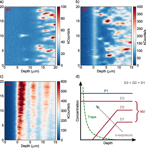
Figure 2. Depth scans (x)–(z) by a confocal microscope taken for single-crystal diamond substrates ( , as-polished surface) after 10 MeV electron irradiation and thermal annealing at 950
  , 2 h in high vacuum. Irradiation doses: (a)
  el cm−2, (b)
  el cm−2, (c)
  el cm−2; the scanned area is 20
  . The scale in depth is given by the positioner of the piezo-scanner. The surface of the samples is at zero position in depth. The scans (a) and (c) are taken from two separate parts cut out of the same substrate. (d) Schematic illustration for the effect of near-surface traps for vacancies in diamond on the efficiency of NV formation by electron irradiation.
Download figure:
Standard image High-resolution imageA schematic representation of the trapping effect is shown in figure 2(d). To minimize a potential depletion effect by polishing, samples used in this study for NV depth profiling were subjected prior to implantation to a RIE/ICP plasma in Ar:SF6 atmosphere in order to etch approximately  in depth. Chemical etching in hot piranha solution has been applied after Ar:SF6 etching to restore the O-terminations at the surface.
The PL scan of the substrate after e-irradiation at high dose in figure 2(c) reveals a layered pattern of NVs in depth. Such distribution profiles are typically observed in nitrogen assisted CVD growth [44]. This creates a stepped surface which provides different crystallographic planes that have different uptake in N and causes striations in NV luminescence through the diamond.
4. Results and discussion
4.1. NV profiles by helium-implantation and annealing
In this work we study the evolution of the NV depth profiles by He-implantation in the temperature range of 950  –1200
–1200  . Thermal annealing not only induces vacancies diffusion, but, leads to different type of defects in irradiated diamond depending on the applied temperature range [14]. A reduction of single vacancies up to
  is observed after annealing at 450
  [32, 33, 45, 46]. Single vacancies, immobile at this temperature, recombine with mobile interstitial defects. We account for this effect when estimating the concentration of free vacancies in our model. The main trapping part above 600
  is the vacancy aggregation in di-vacancies complexes [32, 33]. Efficient NV formation occurs at temperature of 800
  or above. A further increment of the temperature up to 1000
  leads a di-vacancies disappearance to the benefit of multi-vacancies aggregates formation [17, 18]. At such conditions, the NV formation can be considered as a competitive trapping of vacancies between nitrogen atoms and vacancies complexes.
The experimental NV depth profiles by helium irradiation in a 100-oriented CVD diamond  are shown in figures 3 and 4. For the experiments in figure 3, the initial condition
  has been ensured by a helium dose of
  , at 7 °-off angle. This produces approx.
  of vacancies at the ion stopping range according to Crystal Trim (C-TRIM) simulation with a displacement energy of 35 eV. The areal densities of NVs in figures 3 and 4 have been converted to a concentration considering the scanning area of
  and the depth steps between 2 consecutive scans.

Figure 3. (a) Depth distributions of NV centres in 100-oriented CVD samples after helium irradiation at 340 keV (a), (b) energy with a dose of  cm−2 at 7 ° off-angle taken after thermal annealing steps at 950 °C (2 h) and 1200 °C (1 h) (sample A). The histograms are acquired using 3D localization of individual NVs in a confocal microscope (150–250 NVs in each profile). The scale of the histogram for 950 °C is reduced by factor 3. (b). Summary of
  values (Hahn-echo) as measured for single NVs within the He-induced profiles in (a) after sequential annealing at 950 °C and 1200 °C temperatures. The dashed circle indicates a group of 'low-
 ' NVs (approx. 1/3 of total) which disappeared after 1200 °C annealing.
Download figure:
Standard image High-resolution image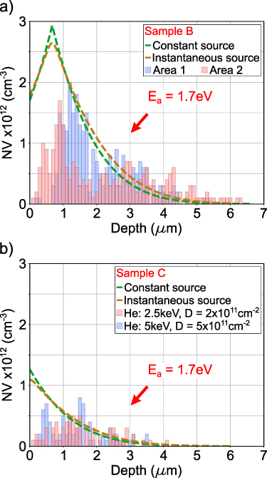
Figure 4. Two depth profiles of NV centres taken at two different areas of 100-oriented CVD diamond after helium implantation (340 keV,  cm−2, 7 ° off-angle) and 1200 °C/1 h annealing (sample B). The two curves represent the fit by the model of vacancy trapping (equation (6b
)) at the boundaries of constant concentration (green curve) and instantaneous planar source (yellow curve). Both fittings yield the activation energy for vacancy diffusion of about 1.7 eV. (b) NV depth profiles at two different areas of a CVD sample similar as in (a) after He implantation at 2.5 keV and 5 keV and 1200 °C annealing. The dashed curves represent the modelling fit at the same boundary conditions.
cm−2, 7 ° off-angle) and 1200 °C/1 h annealing (sample B). The two curves represent the fit by the model of vacancy trapping (equation (6b
)) at the boundaries of constant concentration (green curve) and instantaneous planar source (yellow curve). Both fittings yield the activation energy for vacancy diffusion of about 1.7 eV. (b) NV depth profiles at two different areas of a CVD sample similar as in (a) after He implantation at 2.5 keV and 5 keV and 1200 °C annealing. The dashed curves represent the modelling fit at the same boundary conditions.
Download figure:
Standard image High-resolution imageThe NV profile after annealing at 950  for 2 h shown in figure 3(a) (blue histogram) follows the vacancies distribution by C-TRIM for the same experimental conditions. Here, it is necessary to mention, that NV depth by He irradiation and 950
  annealing is limited mostly by local trapping of vacancies within the initial ion-implanted region (see also figure 6 discussed below).
This conclusion is also confirmed by the statistics of  (Hahn-echo) measurement taken at the corresponding NV profiles. The Hahn-echo sequence was applied at an external magnetic field of 120G. As shown by the blue dots in figure 3(b), approx.
  of the total analyzed NVs show a
  and a noticeable component of
  in the PL spectra. On the other hand, a spin coherence time up to
  can be observed for NVs distributed most probably deeper in the bulk indicating a reduction in the lattice damage. The similarity between the NV profile and the helium stopping range, along with the low
  suggests that trapping of vacancies due to aggregation in the vicinity of radiation defects (i.e. within the helium stopping range) occurs at a faster rate than the projected macroscopic diffusion. This result is in accordance with the model which predicts a high density of di-vacancies and multi-vacancies complexes within the stopping range of helium atoms.
A subsequent annealing of sample A at 1200  for 1 h generates the NV profile shown in red histogram in figures 3(a) and 4. Note, that the two scans after 950
  and 1200
  annealing steps were made at approximately the same area of the sample. Similar NV profiles at the same conditions for another sample (sample B) are shown in figure 4(a). Here the NV depth profiles collected from two different regions are characterized by a depth
  , which is a demonstration of the long range diffusion of vacancies from the initial irradiation damaged area.
As a result of higher temperature annealing, three effects are observed: (i) the vanishing of NVs with low  (see figure 3(b)), (ii) the deeper profile of NVs into the bulk, and (iii) the inhibition of pre-existing NVs in the region damaged by implantation (two histograms in figure 3(a)).
The disappearance of NVs with  suggests a reduction of lattice damages within the He stopping range, which has been achieved through elimination of residual implantation related paramagnetic defects and vacancy chains dissociation [14]. Additionally, an improvement of the spin coherence time up to
  is found for NVs created in the deep tail (depth
  ). This indicates that no competing formation of
  defects takes place (at least in a range of detectable concentration, like in the stopping range at 950
  , where
  prevail). The initial irradiation damaged area, therefore, operates as a vacancies source. Here, indeed, single vacancies are released from chains and diffuse into the bulk to a depth
  . The longer vacancies range diffusion is explainable with an increase of the amount of jumps per single vacancy compared with annealing at 950
  for 2 h as described by equation (4).
The increase of the NVs depth distribution and of the spin coherence time for annealing at 1200  suggests that vacancy diffusion occurs much faster than vacancy aggregation in the deep tail. Hence, in this case the formation of vacancy complexes can be considered negligible compared to that of NVs. Based on these arguments, we modified our model in order to extract the activation energy of vacancy diffusion by fitting the deep tails of the NV distribution. We consider the case of a remote source of vacancies, which is located within the stopping range of He atoms. In a region away from this source, the concentration of NVs at each point of depth will be given by the product:

where [P1] is the local concentration of substitutional nitrogen donors taken as constant through all depth. Here, the vacancy trapping on nitrogen donors is assumed to be not limited by multivacancy defects, as in equations (6a
) and (10). The  function depends on the chosen model of vacancy source. We consider two opposite cases: instantaneous or constant [36]. An instantaneous source is characterized by a 'flash-like' emission of vacancies, which is much shorter than the duration of the annealing process. This emission can be described as

A constant source, instead, is characterized by a vacancies emission comparable with the duration of the annealing process:

The results of the model are shown by dashed lines in figure 4(a). Both approaches yield a vacancy diffusion activation energy of about 1.7 eV, which is quite consistent with earlier estimates [38]. This value is close to the theoretical estimates of energy barrier for di-vacancies formation in diamond [47] ( of the lowest path in the calculation). Therefore, as previously discussed, we can consider the capture cross section for the di-vacancy defect to be close to the geometrical one,
  . The factor 4 stands here for the number of bond directions in
  lattice. It is also worth to note, that the use of the equation (12) or (13) to fit the Ea
directly from NV profiles might not be correct: such functions describe, indeed, only the diffusion of vacancies. The resulting NV profiles in our study, instead, is a product of two separate processes: vacancy diffusion and vacancy trapping on P1 at each point of depth.
lattice. It is also worth to note, that the use of the equation (12) or (13) to fit the Ea
directly from NV profiles might not be correct: such functions describe, indeed, only the diffusion of vacancies. The resulting NV profiles in our study, instead, is a product of two separate processes: vacancy diffusion and vacancy trapping on P1 at each point of depth.
As mentioned before, the additional annealing at 1200  not only generates long vacancies diffusion, but, also induces a reduction in the concentration of the NVs already formed in the area damaged by ion implantation. Similar NVs quenching phenomenon has been widely reported in literature [14, 15, 48, 49] as a consequence of annealing at temperature higher than 1000
  . One possible reason for NV quenching could be the formation of NVH defect. To prevent this defect from depleting NVs, samples A and B were pre-annealed at 950
  for 2 h before ion implantation. This pre-annealing step aimed to remove any residual atomic hydrogen from the lattice after CVD growth process. On the other hand, the increment of the spin coherence time measured in the ion damaged region suggests the absence of states in the energy bandgap that could electrically compensate NVs. Indeed, defects which induce electronic states in the bandgap for charge trapping would also lead to a reduction of electron spin coherence of the NV centres in the vicinity.
A possibility of vacancies surface recombination has been excluded through NV depth distributions generated by low energy ion implantation (figure 4(b)). Electronic grade  CVD diamond (sample C) has been Helium implanted with a dose of
  cm−2 and
  cm−2 respectively at 2.5 eV and 5 eV. A micro-beam ion implanter with coaxial optics for sample alignment has been used, with a nominal-off angle of approx. 7 °. The low implantation energy provides, in accordance to C-TRIM simulation, a vacancies distribution restricted to 10–20 nm below the surface. Figure 4(b) displays the NV depth profiles obtained from sample C following the same annealing procedure as samples A and B. These profiles reveal a formation of NVs that extend up to
  into the bulk, providing further evidence that vacancies do not exhibit a preference for surface recombination. Furthermore, the deep tails of the NV profiles can be accurately modelled using an activation energy of 1.7 eV.
Thus, the reason behind the reduction of NV density could be related to single vacancies which are released at 1200  from previously formed
  defects, and which diffuse deep in the bulk thus forming single NVs visible in the depth tails in figures 3 and 4. These vacancies bind with NVs to form the
  defect [50, 51]. Alternatively, near-surface traps, might bind electrons from NVs and render them unobservable by optical means. The presence of traps combined with different capturing cross section per defect could explain the low P1 to NV conversion efficiency associated to ion implantation technique.
4.2. NVs in bulk by e-exposure: capture cross-section of vacancy trapping
Once the diffusion activation energy is verified, the ratio of  , previously discussed, can be deduced through the experiments on electron exposure. Deep in the bulk NVs are not influenced by any surface-related effects and are far from the depletion region (see figure 2). For this purpose we irradiated several 100 oriented CVD diamond substrates (1ppb) with 10 MeV at different doses.
Samples were irradiated with a 10 MeV linear electron accelerator (MB10-30MP; Mevex Corp.), where the dose was determined by means of a graphite calorimeter. The electron fluence then was re-calculated taking into account the mass collision stopping power in the corresponding energy range.
To estimate the density of as-irradiated vacancies, we used data from reference [52] for vacancy conversion of 3.42 vacancies per electron cm−1 for 10 MeV electrons in diamond. This has been further used to evaluate the initial amount of vacancies produced by a particular dose, and which was considered as reduced by  to consider the effect of vacancy-interstitial recombination at lower temperatures of about 400
  [32, 33, 45, 46]. We estimated the NV concentration deep in the bulk below the NV depletion region by 3D PL mapping technique, as for the NV profiles discussed above. For elevated electron doses, the NV concentration has been evaluated by comparing the photoluminescence intensity collected from such maps with the one of a single NV. The measured NV concentrations have been fit by the model considering only the NV and
  formation. Equation (6b
) has been used for the case
formation. Equation (6b
) has been used for the case  . In the case of low dose exposure,
  , instead, the effect of
  formation can be considered negligible compared to that of NV (
 in equation (5)). Under this assumption the rate of NV formation can be described as

As shown in figure 5 by the dashed curves, the fit provides a NV capture cross section of  , where the vacancy chain capture cross section has been set as the geometrical one,
  . In addition to the data on low-ppm CVD diamond, figure 5 includes also the data on electron exposure of CVD diamond crystals with nitrogen doping in the range of 1 ppm. These samples were produced by CVD in a microwave-plasma-assisted synthesis with 100 major faces containing neutral substitutional nitrogen of approx. 1 ppm. The nitrogen concentration was determined by ultraviolet-visible absorption measurements at 77 K [53]. Different irradiation doses applied to each sample within a range of
  showed NV concentrations ranging from 180 to 430 ppb.
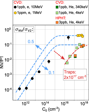
Figure 5. Summary of the experimental data on NV-to-P1 ratio for various CVD and HPHT diamond substrates versus the concentration of initial vacancies C0 as calculated for each experimental condition. For the data on electron exposure the values of C0 are given by the damage model in [51], and for helium implantation by C-TRIM simulation (the values at peak). In all cases the values of 'as-induced' vacancies by the calculations were reduced by  , to account for vacancy-interstitial recombination at lower temperatures, as noticed in [32, 33, 45, 46]. All experimental data points are related to the annealing at 950 °C (2 h). The purple and blue dashed curves are fitting of the data on electron exposure in the bulk by equation (6b
) for two
, to account for vacancy-interstitial recombination at lower temperatures, as noticed in [32, 33, 45, 46]. All experimental data points are related to the annealing at 950 °C (2 h). The purple and blue dashed curves are fitting of the data on electron exposure in the bulk by equation (6b
) for two  ratios of 0.1 and 0.5. The red dashed curve provides fit of the data on helium implantation using the model of near-surface traps by equation (15). The data on 4 keV helium implantation in 1 ppb CVD sample are related to the previous publication in [29].
Download figure:
Standard image High-resolution imageThe results of the modelling establish that vacancies aggregation in multi-vacancy complexes occurs with higher probability than the NV formation. It can be noted here that the conclusion on the low capture cross-section of NV trapping agrees also with the results of theoretical calculations on defect formation energies in diamond [34]. Thus, one would require unavoidably a high dose of electron exposure to activate NVs in diamond bulk by irradiation. Only a small portion of vacancies will be trapped on P1, while the rest will form  .
.
4.3. NV by helium implantation. Limits due to near-surface traps
The obtained data on the vacancies diffusion activation energy and the capture cross section allows us to describe the NV formation within the near surface region. As already discussed, an example of such analysis is shown in figure 6, where a CVD grown electronic grade  diamond (sample D) has been implanted with Helium at 340 keV, with a dose of
  cm−2 and subsequently annealed at 950
  for 2 h. The dose was chosen in order to have a minimum radiation damage but still affordable NV statistics in such low nitrogen doped substrate. The NV depth profiles for different offset implantation angles, (nominally 0 ° and 7 °) are shown by histograms in figure 6. According to the model, even assuming a partial loss of vacancies by trapping within the implantation-related clusters and the lowest
  ratio of 0.1, the P1 to NV conversion efficiency should be
  . The reason behind the relatively low NV yield might be related to addition effect of near-surface traps, responsible for subsurface NV depletion region of electron exposed diamond crystals at low doses (see figure 2). To estimate the traps concentration, we introduce them in our model, assuming their capture cross section identical to that of
 . The introduction of traps modifies the NV formation equation such as

where  represents the concentration of vacancies in trapped into vacancy complexes after n number of jumps. Fitting the experimental data yields the concentration of about
  cm−3 when
  . The results on the traps modelling are summarized in figure 5 as well. It shows the experimental data on 340 keV He irradiation in nominally 1-ppb CVD diamond with as-polished surface, and also the data on 4 keV Helium irradiation taken from our earlier work in [29]. Here we include also the data on the complimentary measurement on HPHT diamond crystal with approx. 3 ppb nitrogen doping exposed to 4 keV Helium at the similar range of doses as in [29]. The sample was grown by the temperature gradient method at 5.5 GPa and
  by using Co-Fe solvent with Ti added as a nitrogen getter. The (100) plate was obtained by laser-cutting and polishing with diamond fine powders. For quantifying the low concentration of nitrogen donors, rapid-passage technique of continuous wave electron paramagnetic resonance (cw-EPR) was employed [54].
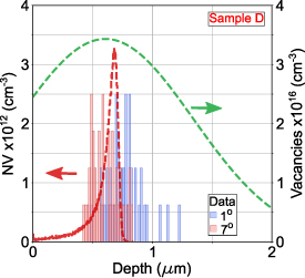
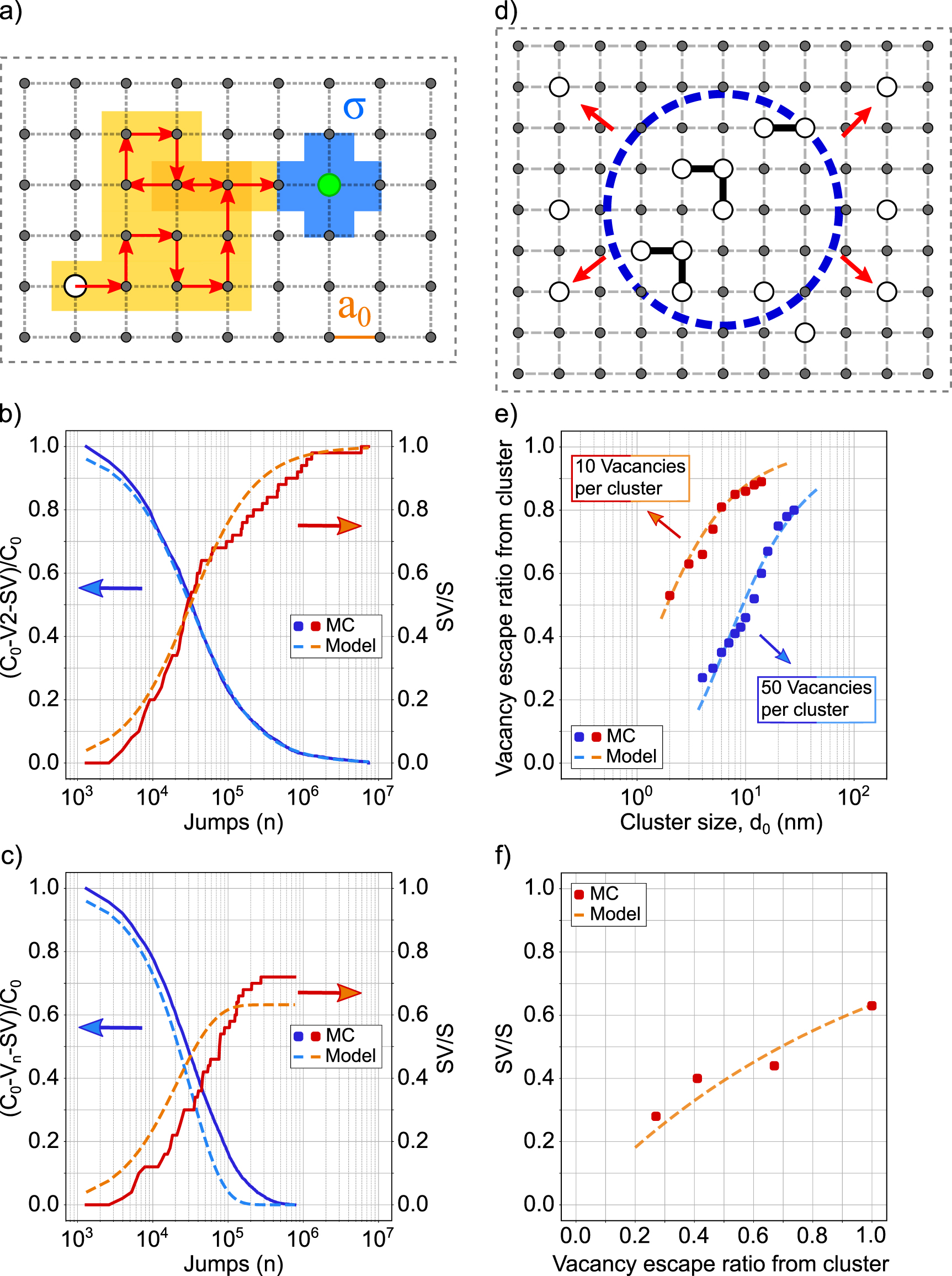
Figure 6. NV depth profiles (blue and red histograms) at a low-dose limit of helium implantation: energy of 340 keV, dose of  cm−2 and nominal off-angles of 1 ° and 7 °, taken after 950 °C annealing for 2 h. The red dashed curve is a profile of NV after trapping in 100-oriented diamond for 340 keV helium and 7 ° off-angle. The green dashed curve represents a projected profile of vacancies calculated for out-diffusion from the initial 'as-implanted' profile by C-TRIM (7 °-off) for the given conditions of annealing (950 °C, 2 h, Ea = 1.7 eV).
Download figure:
Standard image High-resolution image
The C0 in this graph is related to the maximum concentration of vacancies by C-TRIM simulation. The final value shown on the graph had been reduced by  to account for vacancy-interstitial recombination as for the case of e-exposure as discussed above. Regarding the data points on NV-to-P1 ratio for 4 keV experiments, we used the peak concentration of NVs as evaluated from the NV-depth profiling at some irradiation doses in [29]. In summary, the dash-dotted curves 'Traps' in figure 5 shows the fitted NV conversion ratio for a traps concentration of approx.
  cm−3 when
  . The derived value of traps concentration is in a similar range as that estimated from the dose limits shown in figure 2. It is possible to observe that the trap concentration fits approximately all data points related to CVD and HPHT diamonds. The origin of these traps could be related to an initial surface polishing procedure for both CVD and HPHT substrates. In these regards, the method of NV depth profiling in PL scans might help to identify their origin and to find a way to handle it in the future.
5. Conclusion
In this paper we investigated some aspects of vacancies diffusion in diamond lattice with focus on the efficiency of NV formation though vacancy trapping at the nitrogen donor atoms (P1 centres) upon thermal diffusion. To study the limits of the P1-to-NV conversion by this technique we developed an atomistic model of vacancy trapping in a crystal lattice. This model is based on probabilistic atomic jumps, considering competitive trapping of mono-vacancies between di-vacancies  , or multi-vacancy complexes
  and targeted NVs. In the model, we defined the probability of a defect to trap a vacancy as the defect capture cross section. The validity of this approach was verified by Monte-Carlo simulation of various trapping scenarios in a 3D lattice.
The results of modelling were applied to experimental NV profiles generated in CVD and HPHT diamond substrates upon electron exposure, or helium implantation and subsequent thermal annealing. In particular, several electronic-grade CVD diamond substrates were implanted with helium ions at 340 keV and also 4 keV energies and subsequently annealed at 950  and 1200
  temperatures. The resulted NV depth profiles were analyzed using 3D localization of individual NVs in a confocal microscope and sampling their spin coherence properties
  to identify the local environment of trapping centres. In addition, we measured the NV density in the bulk of CVD diamonds with nitrogen doping at low-ppb and low-ppm levels, subjected to MeV electron exposures in a wide range of doses.
Applying the model to the experimental data we estimated the activation energy of vacancy diffusion in diamond about 1.7 eV, which is close to earlier estimates in the literature. The ratio of defect capture cross sections related to di-vacancy  and NV
  and defined as
  was about 0.1–0.5. This result demonstrates the tendency of vacancies to aggregate together rather than being trapped by nitrogen, defining this way a limit of the classical approach in the NV formation by ion implantation or electron irradiation followed by annealing.
In addition, details on NV depth profiling by helium irradiation allowed to get an insight into dynamic of vacancy trapping in diamond. It has been confirmed that vacancy aggregation within ion stopping range at about 950  annealing dominates over macroscopic diffusion due to high density of prime radiation damages. During the subsequent annealing at 1200
  these aggregates can be regarded as a source of vacancies which can diffuse to a depth of several µm and activate NV centres by trapping. Due to the intact lattice environment, the spin coherence time of such deep NVs ranges up to
  in the used CVD substrates.
Finally, we observed two subsidiary effects: (i) the density of NVs within the ion stopping range by helium implantation was noticeably reduced upon 1200  annealing. At the same time, the NVs with low
  below approx.
  disappear. This effect can be related to formation of
  defects formed by release of single vacancies from the initial vacancy aggregates located at the nanometer proximity to the 'low-
 ' NVs. Further investigation of this effect could be beneficial in understanding the origin of a low yield of NV centres by low-energy nitrogen implantation.
(ii) Another effect was related a subsurface NV depletion region observed in the electron irradiated samples at low dose of irradiation. Since the recombination of vacancies at the surface as the main path of extinction was experimentally excluded, we proposed alternative traps in the model to explain the presence of such depletion region. The origin of traps could be related to pre irradiation polishing procedure, however reliably identifying the cause requires further investigation.
The presented model, by virtue of its probabilistic approach, could be used in the future as a tool for engineering the production of other defects in diamond.
Acknowledgment
This work has been supported by the DFG via the FOR2724 and the GRK2624, by the BMBF via Qsens and by EU via the AMADEUS Project.
Data availability statement
All data that support the findings of this study are included within the article (and any supplementary files).
Supplementary data (1.6 MB PDF)