


Abstract
Defects play significant roles in spin-current-related physical processes in intrinsic ferromagnetic semiconductors (FMSs), which are great promise for spintronics applications. However, current defect calculation methods cannot be used to investigate charged defects in FMSs due to the spin polarization of both the charged defect states and ionized carriers, which is not well treated in current defect calculation methods. In order to solve this problem, we propose a spin-distinguishable charge correction (SDCC) method that uses spin-polarized band edge charge density instead of spin-unpolarized uniform background charge density as the compensating charge for charged defects. We apply our method to study the defect properties of CrI3 monolayer and find it can be doped n-type under the Cr-rich growth condition but difficult to be doped p-type. The SDCC method proposed here is generally suitable for all FMSs, which will be useful for the studies of defect properties of magnetic semiconductors.
Export citation and abstract BibTeX RIS

Original content from this work may be used under the terms of the Creative Commons Attribution 4.0 license. Any further distribution of this work must maintain attribution to the author(s) and the title of the work, journal citation and DOI.
1. Introduction
Spintronics has attracted numerous interests in recent years due to their unconventional properties and great promise for high-performance multifunctional applications, such as magnetic random access memory [1–4], logic devices [5, 6], and quantum computation [7]. Recently, semiconductor spintronics has also achieved remarkable successes in the past decades [8, 9]. More and more interests have turned to focus on intrinsic ferromagnetic semiconductors (FMSs), such as CrI3 [10–12]. Compared with dilute magnetic semiconductors, intrinsic FMSs exhibit more stable and ordered magnetic structures and have a longer spin-flip length which depends greatly on the concentration of spin carriers. To further utilize FMSs for spintronic applications, one key issue is to efficiently manipulate the spin-polarized carrier concentration [13, 14]. The same as in non-magnetic semiconductors (NMSs), carrier manipulation in FMSs depends on the defects, whose effects contain providing free carriers to acting as undesirable carrier traps and nonradiative recombination centers [15, 16]. However, it is often very complicated for experiments to study defect properties in magnetic semiconductors, and thus theoretical calculations are necessary to accurately identify the effect of each defect. Based on our knowledge, most of research works on FMSs focus on understanding the magnetic properties [17–19], while carrier-related properties have never been discussed previously in the literature. One of the reasons is that the ionized carriers resulted from charged defects in FMSs are spin-polarized, which is out of present scopes of defect calculations.
Among all the defect-related properties, defect formation energy and ionization energy (IE) are the two most important key quantities. The former determines defect concentration under equilibrium conditions; the latter, determines the ability of a defect to provide carriers. To determine defect IE with different spin polarization, both formation energies of neutral and charged defects with different spin-polarization should be known. Usually, first-principles defect calculations based on density functional theory (DFT) are performed by creating one single defect in a sufficiently large supercell under the defect dilute approximation. For a neutral defect, the formation energy can be accurately obtained. For a charged defect, however, the calculation becomes more complicated for FMSs than NMSs because both the charged defect state and the ionized electron are spin-polarized. Currently, the charged defect calculations in NMSs are usually carried out using the jellium model method, which introduces a uniform background compensating charge density in the whole supercell to represent the ionized electron and keep the system neutral. Nevertheless, the uniform background charge is spin-unpolarized and cannot describe the real ionized electron with spin-polarization in FMSs. Besides, the background charge is distributed uniformly in the whole supercell and results in convergence problems in low-dimensional systems. Although many corrections can be made by constructing artificial potential [20–22] or extrapolating the asymptotic function (WLZ method) [23–27] to solve the convergence problem, these methods cannot deal with the spin polarization of the ionized electron in FMSs since they are still based on the jellium model. Recently, the method proposed by Wu, Zhang, and Pantelides in principle is able to distinguish the spin states of the ionized electron in charged FMSs with defects by constraining the electron occupation numbers of the spin-polarized defect states and band edges [23–27]. However, this method can only accurately capture the real band edge states using a very large supercell [25]. During the past decades, researchers have tried to do some calculations for charged defects using jellium model in FMSs without considering the properties of ionized electrons with spin polarizations [17, 28]. As far as we know, a more practical method considering the spin-polarization of both the charged defect states and the ionized electrons is still lacking for accurately and conveniently calculating the defect properties in FMSs.
In this paper, by considering the spin polarization of the ionized electron, we introduce a general and self-consistent spin-distinguished charge correction spin-distinguishable charge correction (SDCC) method to calculate charged defects in FMSs. The main idea is to use the spin-polarized band-edge charge, instead of the spin-unpolarized and uniformly distributed background charge, as the compensating charge to make the effective charge correction for ionized defects. By doing this, we show that the total charge density in our method is exactly the same as the real charge density for an ionized defect in FMSs. Using CrI3 monolayer as an example, we apply our method to study charged defects in FMSs for the first time. We find that CrI3 monolayer is carrier scarcity under the Cr-middle condition, which is consistent with experiment results [4]. Due to the low formation energy and shallow defect transition levels of  and
and  , the CrI3 monolayer could be doped n-type under the Cr-rich conditions. Nonetheless, it is difficult to dope CrI3 p-type using either intrinsic defects or extrinsic impurities such as group VIA elements substituting I atoms due to the deep defect transition energy levels.
2. Calculation methodology
In an FMS, the band edges including the conduction band minimum (CBM) and the valance band maximum (VBM) states are spin-polarized, as seen in figure 1(a). When a donor (acceptor) is excited, an electron (hole) will be created at the CBM (VBM), which is also spin-polarized. Note that, depending on the excitation manners, i.e. thermal or optical excitations, the ionized electron can be spin-up or spin-down, as seen in figures 1(b) and (c), which clearly show the necessity of considering the spin directions of the ionized electron in an FMS with a charged defect. To do this, we consider the physical process of the ionization (using a donor as an example), that is, an electron is removed from the spin-polarized defect state and finally occupies the spin-polarized band edge state after relaxation. Accordingly, the total charge density has a change of  compared to the neutral state, where
  and
and  are the partial charge density of the spin-polarized CBM and defect states, respectively. With this in mind, we can modify the charge density from the initial neutral defect state by adding
  to mimic the charged defect state. Note that, the spin polarization of the ionized electron can be implicitly included in
  . Another point is that the ionized electron is usually very delocalized with the charge density distributed across the whole supercell, and therefore the spin interaction effect can be reasonably neglected.

Figure 1. Diagrams to show the ionization process of a donor defect and the calculation procedures. (a) The neutral state, (b) the charged state with spin-down ionized carrier, and (c) the charged state with spin-up ionized carrier of a donor defect, respectively. (d) The sketching flow chart for the self-consistent calculations of charged defects in FMSs in our SDCC method.
Download figure:
Standard image High-resolution imageTo realize the above idea in the framework of the DFT, we need to consider the followings. First,  needs to be determined. Under the defect dilute condition, the CBM state is assumed unperturbed with the presence of defects. Therefore,
  can be obtained through
  from the perfect supercell without any defects. It is noteworthy that usually one cannot find the exact CBM state in a small defective supercell due to the couplings between electronic levels [23, 25]. Unlike NMSs, the CBM state in an FMS is spin-polarized and can be spin-up or spin-down, which depends on the spin state of the ionized electron. Under thermodynamic equilibrium condition, the ionized electron will occupy the lower CBM state. However, in some cases, i.e. during optical excitations, the ionized electron can also occupy the higher CBM state to conserve spin momentum. Nevertheless, we can choose the corresponding spin-polarized state to construct
  . For the determination of defect transition energy levels, the lower CBM state should be used.
Subsequently, we need to know  . Since the Kohn–Sham equations are iteratively solved in the DFT code, the level of the spin-polarized defect state will be changed, and thus
  should be calculated at each electronic step. In another word, to mimic the ionized defect state starting from the neutral defect state with a total number of N electrons, the charge density correction
  needs to be conducted at each electronic step. However, it is not always easy to identify the defect state during the iterative process. What is more, even if the charge density is corrected, the electronic states are still occupied by electrons according to their energy orders. In this case, the donor defect state is still occupied while the CBM state is still empty. This will lead to the calculation errors for forces because according to the Hellmann–Feynman theorem, the accurate calculation of forces on ions requires not only charge densities but also wavefunctions of occupied states.
To solve the above difficulties in updating  and calculating forces, we propose to start from the (N − 1)-electron system instead of the neutral N-electron system to mimic the ionized defect state. In this situation, the total charge density for the ionized donor state can be expressed as
  with
with  , which equals to
 in the N-electron neutral defect state and also equals to the practical case. Note that both the ionized donor state and the CBM state are unoccupied in the (N − 1)-electron system, which is different from the practical case that the ionized donor state is empty and the CBM state is occupied. Nevertheless, the CBM state is often delocalized and thus contributes negligibly to the force calculations in the framework of the Hellmann–Feynman theorem.
Based on the above discussions, we can see that by adding the charge density of the corresponding spin-polarized CBM state to the total charge density in the (N − 1)-electron system, we can obtain the correct charge density to describe the charged defect system with spin-distinguishable ionized carriers, and in the meantime reasonably calculate the forces on ions for structural relaxations. The method is named as SDCC method, and implemented in the Quantum Espresso code [29]. The flow chart of our method is given in figure 1(d). It needs to emphasize that the  is added at every electronic step to make sure the total charge density is always corrected to be equal to the practical case.
3. First-principles calculation details
The method is then utilized to study CrI3 monolayer, an intrinsic ferromagnetic semiconductor that has been obtained by mechanical exfoliation and become an emerging material recently [10, 30]. Although many works have explored the potential of CrI3 for spintronic applications [31–33], the investigation of its carrier properties is still deficient because the knowledge of its defect properties is not built due to lack of defect calculation methods for ferromagnetic semiconductors. Now the problem can be solved using our SDCC method. We use the norm-conserving pseudopotentials within the Perdew–Burke–Ernzerhof framework [34, 35] to treat the valence electrons. For the Brillouin zone integrals in the reciprocal space, the single Γ point is used for all calculations, which is accurate enough as the defect supercell is 3 × 3 × 1. The kinetic energy cutoff of the plane wave basis is 80 Ry and the total energy threshold for the convergence is 10−8 Ry. All atoms are relaxed until the Hellman–Feynman forces on individual atoms are less than 10−4 Ry/Bohr. To include the interactions for the localized 3d electrons of Cr ions, the DFT + U method described by Dudarev [36] with an effective Hubbard U parameter of 0.5 eV is used, which is consistent with previous works [37, 38].
The defect formation energy  can be written as a function of the Fermi level
  and the elemental chemical potentials [39]:

where  and
and  are the total energies of the supercell with a defect α charged
  and without any defects, respectively.
  refers to the total energy of the element
  in its pure stable phase,
  is the chemical potential of element
  referenced to
  and
and  is the number of
  atoms removed from (positive) or put in (negative) the supercell in the process of defect formation. The defect transition energy level
  is the Fermi level
  in equation (1) at which the formation energy
  is equal to that of
  :
:

The  terms are calculated using our SDCC method in all the calculations.
4. Results and discussions
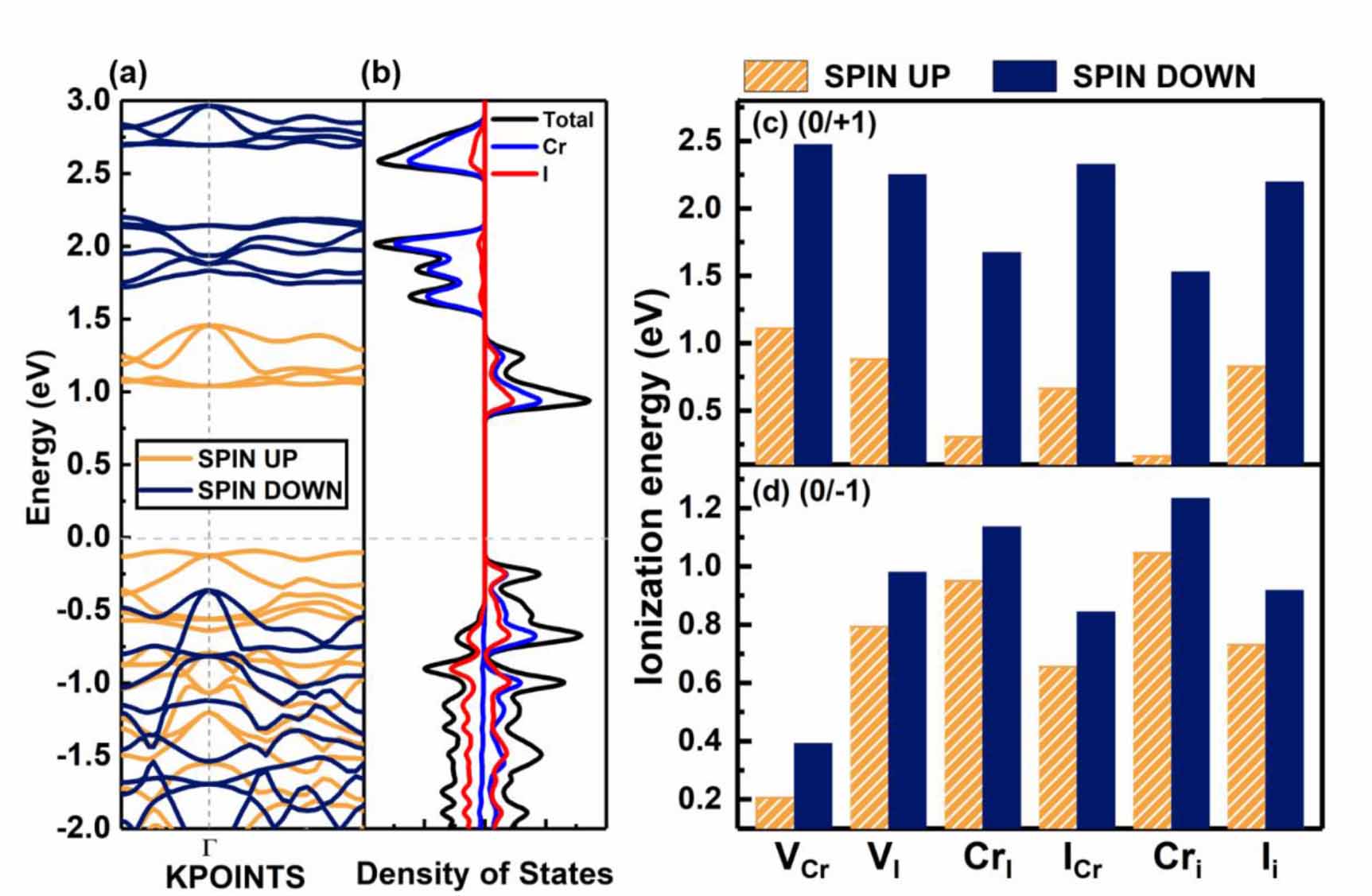
Before starting the defect calculation, we do some calculations to confirm the magnetic ground state. We find that the ferromagnetic state is more energetically favorable, which is 23 meV/formula lower than the antiferromagnetic state, in agreement with previous works [40]. The band structure of the CrI3 monolayer is shown in figure 2(a), in which orange and navy lines represent the spin-up and spin-down channels, respectively. It can be found that the band-edges of CrI3 monolayer are composed of only spin-up states, which is the characteristics of a half semiconductor [41]. The spin-up CBM state is located at the Γ point while the spin-up VBM is located near the Γ point. It is worth noting that both the bands near the spin-up CBM and VBM states are rather flat, indicating that CrI3 monolayer has low carrier mobility due to high effective electron and hole masses (9.968 me for hole and 30.07 me for electron) [42]. However, for the spin-down channel, the effective hole mass (1.96 me ) is much smaller than spin-up channel, which could be useful for spintronic transportations. As seen from the atomic projected density of states and the partial charge density in figure S4, the spin-up VBM and CBM are mainly composed of Cr-3d orbitals and I-5p orbitals and the band gap is about 1.20 eV. For the spin-down channel, the VBM is mainly contributed by I-5p orbitals and the CBM is mainly composed of Cr-3d orbitals. The band gap for spin-down bands is about 2.46 eV. Our calculated electronic properties of pristine 2D monolayer agree well with the previous works [30, 43, 44].

Figure 2. The electronic properties of pristine CrI3 monolayer. (a) The band structure and (b) density of states (DOS) of CrI3 monolayer. (c) and (d) The ionization energies of the intrinsic defects when they are ionized to produce spin-up and spin-down carriers, respectively. Note that, for the positively charged defects, their IEs to produce different spin-polarized carriers can have differences as large as more than 2 eV. For negatively charged defects, they also have small IEs to produce spin-up carriers.
Download figure:
Standard image High-resolution imageBecause the band edges with different spin polarizations have distinctly different charge densities (as figure S3 shown), the defect properties are expected to strongly depend on the spin states of the ionized carriers and charged defects, implying the necessity of considering the spin states of ionized carriers. Here for CrI3 monolayer, we study all the six possible intrinsic defects including chromium vacancy (VCr), iodine vacancy (VI), chromium substituting iodine (CrI), iodine substituting chromium (ICr), chromium interstitial (Cri) and iodine interstitial (Ii) (the full optimized atomic configurations are presented in figure S2). We consider the possibility of these six defects as both donors and acceptors, and calculate the IEs using our SDCC method. It is clear that, if we want to get n-type CrI3, we need to ensure a high enough concentration of Cri and CrI defects due to their small IEs, and the high concentration of VCr defects can achieve p-type doping. Our results show that, when the defects are ionized to produce spin-up carriers, the IEs are much smaller than the cases when the defects are ionized to produce spin-down carriers. Especially, the difference of IEs with different spin-polarized ionized carriers can be larger than 2 eV for positively charged defects. As a result, we mainly consider the cases when the defects are ionized to produce spin-up carriers under the thermodynamic excitation conditions. The optical excitations can be treated as well using our SDCC method.
To make sure the stability of CrI3 monolayer under equilibrium growth conditions, the element chemical potentials should satisfy:

where  is the formation enthalpy of CrI3 monolayer. The dependence of the formation energies of neutral defects on the chemical potentials are given in figure 3. Under the Cr-rich condition, Cri and VI have the lowest formation energies close to 0, which means a large number of these defects are likely to form in CrI3 monolayers under such synthesis conditions. On the contrast, ICr and VCr have the highest formation energies of up to 4.00 eV. Under the Cr-poor condition, ICr antisite and Ii interstitial have the lowest formation energies of less than 1.00 eV. Our calculations provide a quite similar result with [17]. As the chemical potential changes, the formation energies of neutral defects change dramatically, i.e.
  ,
,  , and
, and  can vary by as much as 3.52 eV, 3.52 eV and 2.64 eV, respectively, from the I-rich to the Cr-rich conditions. It is a remarkable fact that there are always some defects with formation energies of less than 1.00 eV in the whole chemical potential range, indicating that CrI3 are prone to have many native defects during synthesis, which have been observed in the previous experiment [45].

Figure 3. The formation energies of intrinsic defects in CrI3 monolayer as a function of chemical potentials varying from I poor condition to I rich condition.
Download figure:
Standard image High-resolution imageFor the charged defects, the formation energies are not only related to the chemical potentials of the elements, but also dependent on the Fermi level position of the material. As shown in figure 3, we choose three chemical potential conditions of the Cr element (Cr-rich condition  eV, Cr-middle condition
  eV, and Cr-poor condition
  eV, details are discussed in SI) to characterize the charged defect properties of the system.
As we can see, the transition energy levels of  ,
,  and
and  are shallow, and hence these defects are the major carrier providers in intrinsic CrI3. Meanwhile, Ii and ICr have deep transition energy levels and they are the major carrier traps. Under thermal equilibrium conditions, the Fermi levels will be pinned at the lowest crossing point of acceptor and donor formation energy [46]. By adjusting the chemical potentials, the formation energies of these defects and thus the carrier types can be tuned. Under the Cr-rich condition (figure 4(a)),
  and
and  can form easily and become the major defects. In this situation, the
  tends to be pinned just below the CBM because if the
  is near the middle of the gap, the donor defect
  and
and  will form and thereupon push the
  upward. On the other hand, if the
  is very close to or above the CBM, the compensating acceptor defects
  and
and  will easily form and pull the
  downward. Therefore, if we want to get n-type CrI3 monolayer, the growth should be carried out under the Cr-rich limit. Differently, under the Cr-middle and Cr-poor conditions (as shown in the figures 4(b) and (c)), the
  is pinned in the middle of the gap due to the competition of intrinsic thermal excitation. In this case, the defect formation energies are always larger than 0.50 eV, indicating the defect and carrier concentration are low. Through the above analysis, we could expect the intrinsic CrI3 monolayer tends to n-type under the Cr-rich growth condition. Interestingly, we found that the spin polarizability of the electrons and holes is independent of the synthesis environment, but related to the temperature (details are discussed in SI).

Figure 4. Formation energies of intrinsic defects in CrI3 monolayer as functions of the Fermi level under the (a) Cr-rich, (b) Cr-middle and (c) Cr-poor conditions. The pinned Fermi level is presented as the red circles and the native thermal excitation is presented as the indigo dash lines. Note that the Fermi level is referenced to the VBM of the spin-up channel and taken as a variable according to the equation (1).
Download figure:
Standard image High-resolution imageBesides the aforementioned intrinsic defects, we also consider doping of extrinsic impurities in CrI3 monolayer. Here, we mainly focus on the cases of anion substituting defects while keeping the Cr sites unchanged to maintain the ferromagnetic properties. We consider to use the VIA elements including O, S, Se, and Te to replace I atoms to see if effective p-type doping can be realized. Our results (figure 5(a)) show that the (0/-) transition levels increase from SI to SeI and to TeI, which are 0.73 eV, 0.76 eV, and 0.82 eV above the VBM, respectively. This is because the defect states are mainly contributed by the VIA p orbitals, which get higher from S to Se and to Te. The OI defect is somewhat an exception with a deeper transition level than SI although O 2p level is lower than S 3p level. This is because, the VBM state is composed of Cr 3d orbital and the p–d coupling between O and Cr is stronger due to the shorter O–Cr bond length. Consequently, the OI level is pushed higher than SI. To demonstrate the above analysis, we split the defect transition energy level into the sum of two parts, which are neutral single-electron defect level ( , the transition of an electron from the VBM state to the defect state) and the relaxation contribution (
 , the lattice and charge relaxation after ionization) [16]:


Figure 5. Group VIA doping in monolayer CrI3. (a) Defect transition energy levels, (b) neutral single-electron point defect levels and (c) relaxation energy costs for OI, SI, SeI and TeI.
Download figure:
Standard image High-resolution image
The calculated  and
and  for VIAI are given in the figures 5(b) and (c), respectively. On the one hand, the neutral defect levels (
 ) increase from OI to SI to SeI and to TeI due to the increased p orbitals of VIA elements. On the other hand, the electron relaxation energies (
 ) decrease from OI to TeI, due to the reduced VIA p-Cr d couplings. The overall effect is that the (0/-) level first decreases from OI to SI and then increases from SI to SeI and to TeI. It is notable that all the acceptor levels caused by VIA doping are rather deep, denoting poor p-type doping in CrI3 monolayer.
5. Conclusion
In summary, we introduce a general and self-consistent SDCC method to describe the charged defect properties in intrinsic ferromagnetic semiconductors by using spin-polarized band edge charge density instead of spin-unpolarized uniform background charge density as the compensating charge. We apply our SDCC method to study the defects properties of CrI3 monolayer, and find it is carrier scarcity under the Cr-middle condition which is consistent with experiment results, but CrI3 monolayer can be doped as n-type semiconductor due to the low formation energy and shallow defect transition levels of  and
and  under the Cr-rich synthesis condition. However, it is difficult to realize p-type semiconductor using either intrinsic defects or extrinsic impurities such as group VIA elements substitutions. The simple and efficient method developed in this work can also be used to study charged defect properties in more complex ferromagnetic semiconducting systems including surfaces and interfaces.
Acknowledgments
This work was partially supported by the China National Key R&D Program (2022YFA1404603), the National Natural Science Foundation of China (Grants No. 11974078, No. 12188101, and No. 11991061) and the Guangdong Major Project of the Basic and Applied Basic Research (Future functional materials under extreme conditions–2021B0301030005).
Data availability statement
The data cannot be made publicly available upon publication because no suitable repository exists for hosting data in this field of study. The data that support the findings of this study are available upon reasonable request from the authors.
Supplementary data (2.0 MB DOCX)