

Abstract
Superconducting circuits based on Josephson junctions have the potential to achieve high speed and ultra-low power consumption, but their integration is limited by the low controllability of Nb-based tunnel junction and the existence of shunt resistors. In this work, we report the fabrication of superconductor/normal metal/superconductor (SNS) Josephson junctions with high reproducibility on oxidized Si substrates. The junctions based on NbN/TaN/NbN trilayers measured at 4.2 K show excellent Josephson properties with a wide range of critical current (Ic) from 227 to 2000 μA. The variations of critical current density (Jc) and characteristic voltage (Vc) are respectively less than 7.1% and 7.5% in the 2 inch region. The standard deviation of Ic is calculated to be less than 1.7% for Josephson arrays with the number of junctions up to 10 000 occupying an area of 0.34 mm2. The results provide a guarantee for the applications of NbN-SNS Josephson junctions in superconducting large-scale integrated circuits.
Export citation and abstract BibTeX RIS
1. Introduction
Josephson junctions play an important role in many large-scale integrated applications of superconducting electronics, including single flux quantum (SFQ) logic circuits, ac and dc Josephson voltage standards, and so on [1–3]. For decades, the most widely studied superconducting integrated circuits were based on Nb/Al/AlOx /Nb tunnel junction due to its high quality and uniformity of up to tens of thousands of junctions [4, 5]. But the shunt resistors are usually required for the tunnel junctions to get critically damped state due to their inherent hysteresis characteristics, which increases the complexity of the process, the area of the circuit and limits the development of integration. One way to avoid shunt resistors is to fabricate junctions with high critical current density (Jc) by decreasing the barrier thickness, which has a large subgap-leakage current to reduce hysteresis [6, 7]. Simultaneously, a large-scale integrated circuit with junctions of high Jc would provide higher operating speed [8]. However, it is difficult to produce reproducibly uniform junctions of high quality because of the very thin oxide layer [9, 10]. Therefore, it is crucial to improve the yield and scale of superconducting circuits by changing the material and structure of Josephson junctions to expect the electrical properties of all junctions to be reproducible and uniform across the circuit area and even across the wafer.
Superconducting niobium nitride (NbN) film has high sheet inductance, which can reduce the area ratio of the transmission line effectively as an alternative to Nb. Furthermore, NbN has a large gap frequency (1.4 THz) and high operating temperature (10 K), indicating that it has great potential for high-frequency and high-speed devices and circuits [11]. However, the studies of tunnel junctions based on NbN film are restricted to epitaxial systems due to the short superconducting coherence length (4–7 nm) of NbN, which largely limits their application on Si substrates [12, 13]. Fortunately, the limitation can be avoided in superconductor/normal metal/superconductor (SNS) Josephson junctions. Because Cooper pairs are transferred in the SNS junction via Andreev reflections at the S-N interfaces [14, 15], the normal metal barriers are approximately ten times thicker than the insulating barriers of the tunnel junctions, allowing for high reproducibility on Si substrates. Simultaneously, the preparation of SNS junction with high quality impose higher requirements on the interface of the trilayer. Hence, nitride materials, such as TaN, NbN and TiN, have been used as the barriers to avoid the formation of compounds across the N–S boundary [16–18]. Thus, the study of NbN-SNS Josephson junctions with high uniformity and reproducibility is of great significance for the development of superconducting large-scale integrated circuits.
In this study, TaN film is used as a barrier because it has similar crystal structure with NbN, which facilitates the high-quality trilayer with clear interface. Furthermore, the electrical properties of the TaN films can be tuned over a wide range by varying the growth conditions, providing the possibility of manufacturing NbN-SNS junctions with different barrier strengths. We prepared uniform NbN-SNS junctions on oxidized Si substrates with high yield and reproducibility. The junctions of different sizes prepared by chemical mechanical polishing (CMP) technology have a wide range of critical current (Ic) to meet various applications and improve the yield of junctions. Finally, we examine the analysis of the uniformity of Ic, Jc, and characteristic voltage (Vc) over a large area. The fabricated SNS junctions have variations of less than 7.5% in a 2 inch region, and the highly uniform arrays contain 10 000 junctions, which is very promising in many fields of superconducting electronics.
2. Experimental
The NbN (200 nm)/TaN (19 nm)/NbN (100 nm) trilayers were continuously deposited on 4 inch oxidized Si wafers at ambient temperature using reactive DC-magnetron sputtering in a cluster deposition system. The sputtering source of NbN and TaN is Nb and Ta, respectively, with a purity of 99.99% and a diameter of 8 inches. The base pressure was 2 × 10⁻⁵ Pa. The NbN films were deposited under the Ar and N2 flow rates of 30 and 8 sccm, respectively. Considering the covering effect of the TaN barrier, we hope that the surface roughness of the based NbN electrode should be as small as possible, also make sure high critical temperature (Tc). The substrates were cleaned with an argon ion beam for 3 min at 150 W before the deposition of the trilayers. The root means square roughness of the 100 nm thick NbN base layer with Tc of 15 K was measured to be less than 1.15 nm over 5 × 5 μm2 using an atomic force microscope, and the height fluctuation of the surface is 7.6 nm. The barrier thickness of 19 nm is precisely controlled by a low sputtering rate of about 0.12 nm s−1 and deposition time. And the Ar/N2 flow ratio is 35:12 with a total pressure of 0.27 Pa. A 200 nm thick NbN film was finally deposited on top as the counter electrode.
The junctions with diameters ranging from 0.6 to 1.6 μm were patterned using i-line stepper photolithography. The specific fabrication process is shown in figure 1. Both the top NbN layer and TaN barrier were etched by inductively coupled plasma (ICP) in a 5 sccm CF4 and 5 sccm Ar mixture to define the junction areas. The etch rate of NbN film is approximately 22 nm min−1 at the ICP power of 100 W, RF power of 10 W, and the pressure of 5 mTorr. The base electrodes were defined by etching the bottom NbN layer using the same way. Then, an insulating layer of SiO2 was deposited by plasma-enhanced chemical vapor deposition at 80 °C. Here the thickness of SiO2 was determined from the thickness of the SNS trilayer and the over-etched SiO2 on substrates, and an additional 100 nm for the following planarization process by CMP. Caldera walls were formed at the edge of the junction areas and base electrode regions by etching SiO2 with reactive ion etching (RIE) in 30 sccm CHF3 gas. The pressure of 2 Pa and the power of 70 W were used to achieve the etch rate of 18 nm min−1. Then the wafer was planarized by CMP to expose the top NbN. RIE is also used to define the contact holes between the base and wiring NbN layer. Before growing the wiring layer, the wafers were cleaned with an argon ion beam for 3 min to remove the impurities and oxide layers on the surface of the junction area. Finally, the counter electrodes were formed by ICP. All wafers are sliced into chips of 5.2 mm × 5.2 mm and bonded with Al wires to the custom printed circuit board (PCB). The electrical properties of the junctions were measured in liquid helium dewar using the four-point method.

Figure 1. Schematic diagram of NbN/TaN/NbN junction process on SiO2/Si substrate.
Download figure:
Standard image High-resolution image3. Results and discussion
3.1. Electrical characteristics of SNS Josephson junctions
Figure 2(a) shows the I–V characteristics of NbN/TaN/NbN junctions with different design diameters from the center chip of the wafer-a measured at 4.2 K. As the junction diameter increased from 0.6 to 1.6 μm, the Ic value, defined as the switching current corresponding to the transition from the zero-voltage state to the normal resistance state, was observed to increase from 227 to 2000 μA. Simultaneously, the I–V curve appeared hysteresis when the junction diameter is larger than 0.8 μm, which was caused by the self-heating of the junction with high Ic [19]. The SNS junctions with a wide range of Ic are suitable for a variety of superconducting electronics applications. For example, the typical critical current (Ic) of the SFQ circuit is designed as 100–500 μA. Large Ic will cause junction self-heating and a need for very low inductances of the loops, making it hard to design the layout. And it is difficult to maintain operational stability in terms of thermal fluctuations when Ic is less than ∼100 μA [1]. For voltage standards circuits, Ic is generally greater than 1 mA to ensure a high operating current margin [20]. The normal state resistance (Rn) decreased from 1.87 to 0.23 Ω, determined by the slope of the normal linear region of the I–V curve as the junction size increased. Then, Vc, the product of Ic and Rn, was calculated to be 0.425 mV, corresponding to the maximum operating frequency of around 200 GHz, related by fmax = Vc/Φ0, where Φ0 is the magnetic flux quantum [21]. Higher Vc can be obtained by decreasing the barrier thickness or increasing the nitrogen content of the barrier [16]. Figure 2(b) shows the dependence of Ic on the magnetic field parallel to the junctions. Ic can be modulated and demonstrate an ideal Fraunhofer-like pattern, which means that the supercurrent flows uniformly through the various junction areas.

Figure 2. (a) I–V curves of the NbN/TaN/NbN Josephson junctions with different design diameters at 4.2 K. (b) Magnetic field dependence of Ic of the junctions in (a). Solid line: the theoretical prediction of Fraunhofer diffraction.
Download figure:
Standard image High-resolution image3.2. Reproducibility of SNS Josephson junctions
The radius of the junction will be reduced compared to the design value (r) on the mask after the steps of the fabrication process, affecting the calculation of actual Jc according to the equation Ic = Jc πr2. Therefore, the pattern shift (dr) of junction radius should be considered when calculating Jc, and the above relationship is modified as Ic = Jc π(r+ dr)2. Subsequently, the values of Jc and dr were obtained from graphs √(Ic/π) versus r, as shown in figure 3. It can be seen that the fitting results from the chips at the same position on three wafers almost intersect at a point on the horizontal axis, from which we calculated dr of −30, −25, and −28 nm, indicating the excellent reproducibility of the process. And such a small pattern shift will reduce the impact on the margins of the circuit parameters. Jc is determined as the square of the slope to be 106, 112, and 99 kA cm−2, listed in table 1 together with Vc. The slight variation in Jc or Vc values is due to the influence of barrier parameters, such as thickness and stoichiometric. Nevertheless, it can be considered that our process has high stability and contributes to the good reproducibility of the junctions.

Figure 3. Fitting curves of √(Ic/π) and design junction radius (r) for test chips at the center of three wafers according to Ic = Jc π(r + dr)2.
Download figure:
Standard image High-resolution imageTable 1. Values of dr, Jc, Vc of SNS Josephson junctions and their variations in the 2 inch range from three wafers with the same preparation conditions. All the properties were measured at 4.2 K.
| Series | dr (nm) | Jc (kA cm−2) | Vc (mV) | Variation of Jc | Variation of Vc |
|---|---|---|---|---|---|
| Wafer-a | −30 | 106 | 0.415 | 7.1% | 7.5% |
| Wafer-b | −25 | 112 | 0.425 | 7.3% | 8.1% |
| Wafer-c | −28 | 99 | 0.408 | 7.1% | 7.3% |
3.3. Yield and uniformity of SNS Josephson junctions
To ensure the stable operation and yield of large-scale integrated circuits, the Ic of the junctions must be highly uniform. Figure 4 shows Ic distributions of SNS junctions calculated from the I–V curves of series arrays on the center chip of the wafer-a. The total Vc values of the arrays were calculated in the same way as that of a single junction and then divided by the number of junctions to obtain the average Vc of all junctions. A series of data points were taken out near the switching current on I–V curves, and the corresponding voltage difference between two points was divided by average Vc to get the number of junctions with the corresponding Ic. The Ic values have normal distributions that are well fitted by a Gaussian distribution. The design diameters of all the junctions are 0.6 μm in figure 4(a). The mean value <Ic> and standard deviation (σI c) of Ic are consistent across all arrays with different numbers of junctions from the same chip, as can be seen from the I–V curves of the junction arrays shown in the illustration. The I–V curves show hysteresis, presumably caused by joule heat generated by the junctions entering the normal resistance state. As the number of junctions increased from 2000 to 10 000, the area occupied by the arrays increased from 0.04 to 0.34 mm2, with the maximum area far exceeding the 0.14 mm2 area reported for the 8-bit ERSFQ parallel binary shifter [22]. Figure 4(b) shows the Ic distribution statistical results of junction arrays with number of 10 000 and design diameters of 0.6, 0.8, and 1.2 μm. All arrays exhibit high uniformity, with σI c values of 1.7%, 1.3%, and 1.4%, respectively. The array with design diameter of 1.2 μm has a worse fit than others due to the influence of noise caused by the ambient magnetic field and flux pinning. The total area of the three arrays with 10 000 junctions is 1.02 mm2, which is larger than the reported 8-bit parallel arithmetic logic unit area of 0.80 mm2 [23]. Therefore, we believe that the variations in our SNS junction arrays are sufficiently low to produce a large-scale integrated circuit.
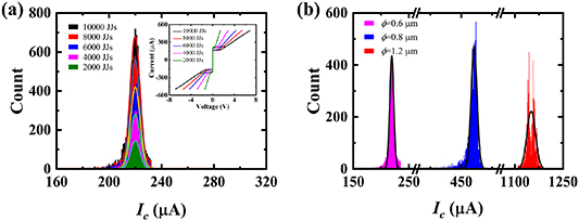
Figure 4. Statistical chart of critical current distribution for NbN/TaN/NbN Josephson junction arrays: (a) the number of junctions ranges from 2000 to 10 000. Each junction is 0.6 μm in design diameter. The inset shows I–V curves of the arrays with different numbers of junctions. (b) The design diameters are 0.6, 0.8, and 1.2 μm, and the number is 10 000. The solid curves are Gaussian fits.
Download figure:
Standard image High-resolution imageBesides the uniformity of junction properties on the same chip, the distribution and yield on the entire wafer are also very important, related to the operating margin of the circuit [24]. Figure 5 shows the spatial distributions of Jc and Vc of NbN/TaN/NbN junctions across a 4 inch wafer. Each square represents a 5.2 mm × 5.2 mm chip. And each Jc or Vc value is the average of the result from the junctions with diameters ranging from 0.6 to 1.6 μm, taking into account the pattern shift produced by the fabrication process. The variations of Jc and Vc were calculated to be only 7.1% and 7.5%, respectively, in the 2 inch range, which for Jc is only the half value of Nb/NbSi/Nb junctions [25]. The high uniformity of SNS junction properties over a large area ensures a possible higher yield of the circuit when applied. It is obvious that both Jc and Vc have a maximum in the center of the wafer and tend to decrease toward the edge, which may be affected by the uneven distribution of TaN barrier components and NbN electrode thickness. The resistivities of TaN films directly grown on the SiO2/Si substrates were measured by the four-point method using a physical property measurement system, revealing a gradual increase from the center to the edge of the wafer. In the normal metal layer with higher resistivity, the wave function of the superconducting layer decays faster, causing the decrease of Jc and Vc [16]. Furthermore, the thickness of NbN film is thinner at the wafer edge. And the Tc or energy gap of NbN film is dependent on thickness when it is less than about 200 nm [26], resulting in the distributions of Jc or Vc in figure 5. In addition, the fluctuations of the thickness of base NbN electrode lead to the change of the interface roughness, which affects the Andrew reflection at the S/N interface [27]. Distribution statistics in the 2 inch range from three wafers are shown in table 1. The variations of Jc and Vc values are consistent across the three wafers, again indicating the high reproducibility of the junctions, which is required for complex circuits.

Figure 5. Spatial distributions of (a) Jc and (b) Vc of NbN/TaN/NbN Josephson junctions across a 4 inch wafer. Each data is the average result of the junctions with diameters of 0.6–1.6 μm. And each square represents a 5.2 mm × 5.2 mm chip.
Download figure:
Standard image High-resolution image
4. Conclusions
In summary, we have prepared NbN/TaN/NbN-SNS Josephson junctions suitable for large-scale integrated circuits using the planarized process on oxidized Si substrates. The Ic values of SNS junctions with excellent Josephson properties are varied in a wide range from 227 to 2000 μA for various superconducting electronics applications. Analysis of the pattern shift demonstrates that our process is very stable. The junctions with a barrier thickness of 19 nm have Jc values of 99–112 kA cm−2, Vc values ranging from 0.408 to 0.425 mV, indicating high reproducibility. Furthermore, the junction array with number of 10 000 has a low variation of less than 1.7% in Ic, occupying an area of 0.34 mm2 in the layout. The device parameters decrease gradually from the center to the edge on the 4 inch wafer, which is mainly caused by the uneven distribution of the components of the barrier and the thickness of the superconducting layer. Nevertheless, the deviations of Jc and Vc values in the 2 inch region are less than 7.1% and 7.5%, respectively. Such a high uniformity of the junctions over a large area ensures the yield and stable operation of the circuits. In a word, the works are favorable for the design and even operation of large-scale integrated circuits based on NbN-SNS Josephson junctions.
Acknowledgments
This work was supported by the 'Strategic Priority Research Program (A)' of the Chinese Academy of Sciences (CAS) (Grant No. XDA18010200), the Frontier Science Key Programs of CAS (Grant No. QYZDY-SSW-JSC033), the Young Investigator Program of the CAS (Grant No. 2016217) and the National Natural Science Foundation of China (Grant Nos. 61801462, 62071458 and 11827805). We would like to thank Ms Yingyi Shao, from Shanghai Institute of Microsystem and Information Technology (SIMIT), Chinese Academy of Sciences (CAS), for useful discussion on the preparation process of Josephson junction.
Data availability statement
The data that support the findings of this study are available upon reasonable request from the authors.