
Abstract
We present a study of radio frequency properties of niobium films deposited on copper by two different approaches based on High Power Impulse Magnetron Sputtering, namely with a DC voltage biased substrate and with bipolar target voltage. Such approaches enable the synthesis of dense superconducting (SC) layers. The SC radio frequency losses of these films are characterized as a function of the applied RF magnetic field using a dedicated calorimetric method. We report on a significant reduction of the Q-slope phenomenon and the residual surface resistance in the characterized films, achieving similar values as those obtained on bulk niobium surfaces qualified with the same technique. Our results pave the way towards the realization of Nb/Cu coated accelerating cavities featuring a surface resistance 2–3 times lower than the state-of-the-art values at working frequencies of 400 and 800 MHz, making this technology even more appealing for future particle accelerators and colliders.
Export citation and abstract BibTeX RIS

Original content from this work may be used under the terms of the Creative Commons Attribution 4.0 license. Any further distribution of this work must maintain attribution to the author(s) and the title of the work, journal citation and DOI.
1. Introduction
Proton and electron accelerators are not only essential for fundamental studies in particle and high energy physics but also in different disciplines as biology, chemistry, solid-state physics [1], and medicine [2]. Advances in superconducting (SC) technology have always been beneficial for the realization of accelerating machines. In particular, the use of superconducting radio frequency (SRF) accelerating cavities has allowed to significantly improve the accelerators performance and to reduce the costs [3].
Bulk niobium SRF cavities are nowadays crucial for both electron and proton accelerators, which are respectively used for the generation of x-rays (e.g. European x-ray free electron laser—XFEL facility in Hamburg [4]), and for neutron spallation sources (e.g. European Spallation Source—ESS in Lund [5]). In fact, they have enabled the production of electron/proton pulses with unprecedented intensity, quality and temporal structure. A real challenge is to satisfy the demand of continuous wave operation and high repetition rates to obtain even higher beam currents. To achieve such specifications, researchers in the field are currently trying to push the performance of bulk Nb RF cavities to their theoretical limits. Limitations can originate both from intrinsic properties of these objects and from environmental variables, such as cooling conditions or the effectiveness of the magnetic shielding around the cryostat. Therefore, to obtain the highest performance, a deep knowledge of the working behavior of the specific cavity, a proper monitoring and a good control of the environment are necessary.
In the search for a reduction in power consumption and for the achievement of larger-accelerating gradients, different alternatives are explored. In spite of the lower accelerating gradients which can be achieved, the niobium film on copper technology (Nb/Cu) represents one of the possible solutions, providing several advantages over the bulk Nb. It guarantees a reduction of the fabrication costs, a better thermal stability at cryogenic temperatures and a lower sensitivity to the ambient magnetic field [6]. Nb/Cu SRF cavities have been already successfully employed for circular colliders as the large electron–positron (LEP) collider [7] and the large hadron collider (LHC) [8], or linear accelerators like the High Energy and Intensity—Isotope mass Separator On-Line facility [9] at CERN or the Alpi accelerator at the LNL of Legnaro. Despite its advantages, this technology still exhibits a behavior known as 'Q-slope' resulting in a degradation of the quality factor of the cavity when increasing the accelerating voltage. This phenomenon is a direct consequence of the increase in the thin-film surface resistance when the latter is exposed to increasing surface magnetic field. At the beginning of this technology, the Nb films were deposited by DC magnetron sputtering (DCMS), as was the case for LEP [10] and LHC [11]. Since then, remarkable efforts have been done to improve the sputtering process as it was known that there is a direct impact on the RF performance [12, 13]. A potential cause of the 'Q-slope' has been identified in the shape of the cavities, that leads to off-normal impinging angle of the sputtered species during the coating process [14]. This induces porosities in the film and degrades its overall SC performances. In this study, we investigate a coating technique known as high power impulse magnetron sputtering (HiPIMS) allowing for the production of metal ions that can be accelerated toward the substrate [15] to densify the growing thin film [16, 17]. Experimental results indicate that this coating technique can provide residual surface resistance at the state-of-the-art for Nb/Cu films. At the same time, a significant mitigation of the 'Q-slope' is observed, with a shallow dependence of the surface resistance as a function of the peak magnetic field in the common operation range of the accelerating voltage.
2. Coating technique and film properties
The coating setup consists of a cylindrical cathode of 45 mm external diameter made out of pure niobium having a residual resistivity ratio of 300. The magnetic field is provided by a 50 mm long and 30 mm in diameter NdFeB magnet inserted in the cathode. The sample is placed at a distance of 80.5 mm from the cathode in order to reproduce the location of a 1.3 GHz SRF cavity's equator. A detailed description of the coating apparatus is given in the supplemental material (available online at stacks.iop.org/SUST/35/054008/mmedia). The chamber is pumped down to a pressure of about 1  mbar. A bakeout is performed over 48 h at 200 ∘C after which the coating chamber and the sample are kept at 150 ∘C while the pumping station is cooled down to room temperature. A base pressure of 5
  mbar is reached prior to coating. Two samples are coated using HiPIMS in two different configurations: the first (HiPIMS + BS) with the application of a bias to the substrate, the second (HiPIMS + PP) with a positive voltage pulse applied at the target during the afterglow keeping the substrate at ground potential. A comprehensive summary of the experimental parameters is given in table 1 with the corresponding voltage and current wave-forms shown in figures 1 and 2.

Figure 1. In blue, the applied cathode voltage pulse for HiPIMS + BS. In red, the corresponding current wave-forms of the cathode (continuous line) and at the substrate (dashed line).
Download figure:
Standard image High-resolution image
Figure 2. In blue, the applied cathode voltage pulse for HiPIMS + PP. In red, the corresponding current wave-form of the cathode.
Download figure:
Standard image High-resolution imageTable 1. Summary of the two coating techniques parameters used in this study.
| Coating technique | ||
|---|---|---|
| Parameter | HiPIMS + BS | HiPIMS + PP |
| Main pulse duration (µs) | 200 | 30 |
| Frequency (Hz) | 100 | 1000 |
| Average power (kW) | 1.2 | 1 |
| Peak current (A) | 150 | 100 |
| Bias voltage (V) | −25/−50 | 0 |
| Positive pulse duration (µs) | N/A | 200 |
| Positive pulse delay (µs) | N/A | 4 |
| Positive pulse voltage (V) | N/A | 80 |
| Sputtering gas | Kr | Ar |
| Sputtering pressure (mbar) | 2.3 
| 7 
|
| Coating temperature (∘C) | 150 | 150 |
| Coating duration (h) | 6 | 6 |
The supplementary material details the samples preparation prior to coating.
After RF testing, the two samples are characterized by x-ray fluorescence in order to evaluate the films thickness. The HiPIMS + BS and HiPIMS + PP films are  m and
m and  m thick, respectively. The samples are also characterized by scanning electron microscopy (SEM) as shown on figure 3. The film surface looks very similar, with strongly faceted crytallites. The coating performed using HiPIMS + PP (figure 3(b)) exhibits a slightly smoother surface. Samples coated in similar conditions as the quadrupole resonator (QPR) were further analyzed by x-ray diffraction as well as by performing SEM cross-section observation after focused ion-beam (FIB) milling. The cross sections are presented in the figure 4. The average grain size at the top layer surface was extrated from the pitctures and a similar value of about 390 nm was found for both layers.

Figure 3. SEM top views of a niobium film coated by means of (a) HiPIMS + BS and (b) HiPIMS + PP. The scale bars represent 2 µm length.
Download figure:
Standard image High-resolution image
Figure 4. FIB cross-sections of samples coated, using similar parameters as for the QPR resonators, using (a) HiPIMS + BS and (b) HiPIMS + PP techniques. The scale bars represent 2 µm length.
Download figure:
Standard image High-resolution imageUsing x-ray diffractograms we performed a full Rietveld analysis of the data using MAUD software [18]. From this analysis we extracted the crystallites size (D), micro-strain ( ) and lattice parameter (a). We then evaluated the dislocation density at the film surface expressed as:
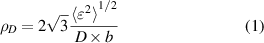
where ρD
is the dislocation density and b is the burger vector expressed as  (m) for BCC materials.
The fitted and calculated data are summarized in table 2.
Table 2. Material parameters extracted from XRD analysis and the calculated dislocation density for the two elaborated Nb films.
| Parameter | HiPIMS + BS | HiPIMS + PP |
|---|---|---|
| Crystallite size (nm) | 91 | 54 |
| Microstrain | 0.00 204 | 0.00 268 |
| Lattice parameter (Å) | 3.30 053 | 3.30 101 |
| Dislocations density (m−2) |

|

|
One can first notice that the crystallites size is much smaller than the grain size and thus most likely to be the driving parameters regarding the defect density such as dislocations. Both films exhibit lattice parameter slightly higher than the bulk Nb which implies a compressive residual stress in the layers, as is usually observed for thin films elaborated by physical vapor deposition [19]. Finally, we notice that both coating techniques lead to films having a high density of dislocations in the range of 1014 m−2 with an even higher value for HiPIMS + PP by more than a factor of 2. We discuss the potential effect of these defects onto the RF performance of the elaborated layers in section 4. It thus appears that despite the very different process parameters used for the elaboration of the two films the surface roughness and grain sizes remain qualitatively comparable. However, the dislocation density clearly appears to differ and may further impact the SRF behavior.
3. RF measurement and analysis methodologies
The CERN QPR is used for the characterization of the RF performance of small flat SC or metallic samples [20–22]. When the QPR is excited at its resonance modes, the RF currents circulating in the rods create an image current on the sample surface placed underneath. All the quadrupole modes (TE21-like) up to 2 GHz are such that the RF fields exponentially decay in the 2 mm coaxial gap around the sample cylinder. The same applies for dipole modes (TE11-like) below 1 GHz [23]. Therefore, one would expect that the power dissipation in the gap and, in particular, at the normal conducting end flange and copper joint, is negligible. However, as discussed later in this work and studied in more details in reference [24], this is not what is observed experimentally and extra dissipation in those normal conducting parts need to be taken into account. The current equipment allows for probing from the fundamental quadrupole mode up to the second harmonic ( MHz,
MHz,  MHz and
  MHz). Such values are typical operation frequencies of most of the existing [25] and under-study accelerators (e.g. the RF systems of the Future Circular Collider (FCC) machines [26]). Indeed, this aspect represents a great value of the QPR. The RF properties of a SC coating, in fact, can be characterized in the whole frequency range of interest without the need of using substrate cavities of different size. For a more detailed description of the QPR and of its working principle, we refer to [23, 27] and references therein.
The surface resistance Rs of the SC material (film or bulk) is the actual physical quantity defining the cavity performance. Note that the Q0 measured in a cavity is directly related to the average Rs of the SC film as follows:
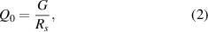
where G is a geometrical factor of the cavity that accounts for the electromagnetic field distribution. Therefore, measuring the Rs
of the SC coating (or of a bulk sample) under investigation qualifies it for application in an accelerating cavity. In this respect, the QPR is a very interesting tool as it allows to measure Rs
as a function of the peak RF magnetic field Bpk
on the sample surface at fixed temperature by means of an RF-DC compensation (or calorimetric) technique. In addition, the temperature dependence of Rs
at a given RF field is also crucial. This is measured by keeping fixed Bpk
while sweeping the temperature by means of the heater. In general, the full response to external RF electromagnetic field is described by the surface impedance  , where the imaginary part Xs
is known as surface reactance. While Rs
is estimated as described above, the surface reactance Xs
can be experimentally obtained from the measurement of the QPR cavity resonance frequency. In fact, within the London theory [28], if the temperature is not too close to Tc
, one can write
, where the imaginary part Xs
is known as surface reactance. While Rs
is estimated as described above, the surface reactance Xs
can be experimentally obtained from the measurement of the QPR cavity resonance frequency. In fact, within the London theory [28], if the temperature is not too close to Tc
, one can write  [29]. Here
  is the effective penetration depth of the electromagnetic field inside the superconductor, with λL
being the London penetration depth, and ξ0 the BCS coherence length. The variation of the penetration depth
is the effective penetration depth of the electromagnetic field inside the superconductor, with λL
being the London penetration depth, and ξ0 the BCS coherence length. The variation of the penetration depth  , with T0 a reference temperature, is directly proportional to the change of the resonance frequency
  as follows [23]:
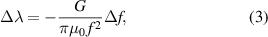
where G is the sample geometry factor that depends on the mode. The change in the resonance frequency  is measured by heating up the sample with the DC heater above the transition temperature, while tracking the mode resonance with a vector network analyzer (VNA). A comparison to theoretical models allows to determine the main SC parameters characterizing the material. In the optimization process of the Nb on Cu coatings, the knowledge of the values of critical material parameters is crucial. The mean-free-path l and other fundamental SC parameters that play an important role on both DC transport and RF performance, being strongly related to the micro-structural quality of the Nb layer, can be extracted from the analysis of
  . To analyze both
  and
and  data we use numerical solutions of the BCS formulation of the RF surface impedance Zs
of a superconductor in the anomalous skin depth regime. The RF response of a superconductor within the BCS framework was first derived by Mattis and Bardeen (MB) [30] using a perturbation approach, in the low field limit. In particular, the real component, representing the RF surface resistance of a BCS superconductor RBCS
is associated to thermally activated quasiparticles, whose density decreases exponentially with temperature. All the remaining loss mechanisms, which dominate at low temperature (
data we use numerical solutions of the BCS formulation of the RF surface impedance Zs
of a superconductor in the anomalous skin depth regime. The RF response of a superconductor within the BCS framework was first derived by Mattis and Bardeen (MB) [30] using a perturbation approach, in the low field limit. In particular, the real component, representing the RF surface resistance of a BCS superconductor RBCS
is associated to thermally activated quasiparticles, whose density decreases exponentially with temperature. All the remaining loss mechanisms, which dominate at low temperature ( ), are generally included in a temperature independent term Rres
, and thus the surface resistance is decomposed as follows:
), are generally included in a temperature independent term Rres
, and thus the surface resistance is decomposed as follows:

where Rres
is referred to as residual resistance. The BCS term RBCS
is a function of the temperature and depends on the coherence length ξ0, the London penetration depth λL
, the mean-free-path l, the SC gap Δ, and the Tc
of the superconductor. A numerical calculation of both the real and the imaginary components of the  of a superconductor was introduced and implemented by Halbritter [31]. This method is commonly used to analyze data from bulk Nb cavities, by fixing both the values of
  nm and
  nm, and varying l and Δ as fitting parameters to be extracted [32, 33]. The critical temperature is estimated independently. As the values of ξ0 and λL
in the case of Nb on Cu coatings depend on the deposition conditions and cannot be set a priori, they also need to be included in the fitting routine. In this work, we follow the procedure described and demonstrated in [34]. Due to correlations among some of the SC parameters, different set of values could provide good agreement between data and theory. In order to prevent non-physical estimations, we search for a set of four fitting parameters that minimizes a combination of the chi-square
nm, and varying l and Δ as fitting parameters to be extracted [32, 33]. The critical temperature is estimated independently. As the values of ξ0 and λL
in the case of Nb on Cu coatings depend on the deposition conditions and cannot be set a priori, they also need to be included in the fitting routine. In this work, we follow the procedure described and demonstrated in [34]. Due to correlations among some of the SC parameters, different set of values could provide good agreement between data and theory. In order to prevent non-physical estimations, we search for a set of four fitting parameters that minimizes a combination of the chi-square  values from both
  and Rs
(T) experimental data.
and Rs
(T) experimental data.
4. Results and discussion
The most important figure of merit of an SRF cavity is the dependence of the unloaded quality factor Q0 with respect to the accelerating gradient Eacc
at a fixed temperature of operation. The unloaded quality factor Q0 describes the ability of the cavity to store electromagnetic energy U, and it depends on the power dissipated on the cavity walls Pc
as follows:  , with
  the operation frequency. For an accelerating cavity both Q0 and Eacc
are directly related via a geometric factor, respectively, to the value of the surface resistance Rs
(2) and the peak RF magnetic field Bpk
. These are the physical quantities that we extract from the experiments performed with the QPR (see section 3). In the following, the RF performance of the investigated samples, as a function of both the field and the temperature for all three different accessible quadrupole modes, is presented and described.
the operation frequency. For an accelerating cavity both Q0 and Eacc
are directly related via a geometric factor, respectively, to the value of the surface resistance Rs
(2) and the peak RF magnetic field Bpk
. These are the physical quantities that we extract from the experiments performed with the QPR (see section 3). In the following, the RF performance of the investigated samples, as a function of both the field and the temperature for all three different accessible quadrupole modes, is presented and described.
First, we report on the study of the temperature dependence of both the real and the imaginary parts of the complex surface impedance Zs
of the investigated samples. In figure 5(a) we show the temperature dependence of  for the HiPIMS + BS coated sample, as obtained from the experimental measurement in transmission of the resonance frequency (400 MHz mode) via a VNA with 10 dBm input power. In figure 5(b), instead, we display the temperature dependence of the surface resistance of the same sample, measured at
  mT for the three different QPR modes. All error bars in the reported Rs data are estimated as the standard deviation of repeated measurements (N = 20). The results as a function of the temperature for the other two samples (bulk Nb and HiPIMS + PP coated) are reported in the supplemental material.

Figure 5. (a) Variation of the effective penetration depth  as a function of the sample temperature for the HiPIMS + BS coating. The solid line represents the best numerical fit to BCS theory. (b) Surface resistance Rs
as a function of the sample temperature for the HiPIMS + BS coating for the three different quadrupole modes: 400 MHz (red), 800 MHz (green) and 1200 MHz (blue). Data are taken at
as a function of the sample temperature for the HiPIMS + BS coating. The solid line represents the best numerical fit to BCS theory. (b) Surface resistance Rs
as a function of the sample temperature for the HiPIMS + BS coating for the three different quadrupole modes: 400 MHz (red), 800 MHz (green) and 1200 MHz (blue). Data are taken at  mT. The solid lines represent the numerical estimates of the BCS surface resistance, obtained with the same fitting parameters for all modes.
Download figure:
Standard image High-resolution imageThe solid lines in figure 5 represent the best numerical fit of the presented data as described in the previous section. Here, we emphasize that the critical temperature can be obtained by fitting the curve in figure 5(a) to the Gorter-Casimir expression. While heating up the sample to cross the transition temperature, radial temperature gradients are generated as the heater is in located at the center of the sample. The temperature sensor is not located in the hottest point, but at half radius approximately, which can lead to underestimations in the measurements. In the case of bulk Nb samples, due to the lower thermal conductivity, the gradients are expected to be higher. However, this has been studied with thermal simulations and they are expected to be negligible also for bulk Nb samples. The parameters obtained by applying the fitting procedure to data at 400 MHz are listed in table 3 for all the investigated samples. Note that the fit is made in order to get a consistent set of parameters fitting the results for all temperatures and frequencies of the measurements. It is important to emphasize that, provided a different Rres for the different modes, the reported data scale in frequency in a very good agreement with what expected from BCS-MB.
Table 3. BCS fitting parameters for the three different investigated samples.
| Sample | l (nm) | ξ0 (nm) | λL (nm) |

|
 (K) (K) |
|---|---|---|---|---|---|
| Bulk Nb | 500 ± 125 | 33 ± 8 | 27 ± 7 | 2.1 ± 0.5 | 9.35 |
| HiPIMS + BS | 160 ± 40 | 28 ± 7 | 23 ± 6 | 2.3 ± 0.6 | 9.1 |
| HiPIMS + PP | 400 ± 101 | 32 ± 8 | 32 ± 9 | 2.3 ± 0.6 | 9.05 |
All the samples are characterized by a long mean-free-path l, especially the bulk Nb, as expected from the large RRR > 100 of the raw material employed for its fabrication. This result demonstrates the high structural quality of the studied Nb coatings. This analysis provides crucial information on the coatings, which can be used together with the overall RF performance to effectively guide the choice of the best Nb deposition recipe to adopt in the future.
We now focus on the field dependence of the surface resistance Rs
. In particular, in figure 6 we show the estimated Rs
values versus the peak RF magnetic field Bpk
at the fundamental frequency  MHz and at two distinct sample's temperatures, namely T = 2.5 K (a) and T = 4.5 K (b).

Figure 6. Surface resistance Rs
as a function of the peak magnetic RF field Bpk
at  MHz, T = 2.5 K (a) and T = 4.5 K (b) for the three characterized samples: bulk niobium (black stars), HiPIMS + BS coating (red triangles), HiPIMS + PP coating (green squares) and LHC PCO4 cavity (orange crosses). The dashed straight lines in (a) represent the best linear fit of the experimental data.
Download figure:
Standard image High-resolution image
At T = 2.5 K all the samples exhibit a linear field dependence of Rs
within the measurement range, with a quite shallow slope (see figure 6(a)). At this temperature and frequency, the residual resistance Rres
dominates over the BCS term, which would only account for 1–2 nΩ. Then, Rs
can be approximated to  , with
  . The dashed straight lines represent the best fit. The obtained fitting parameters are listed in table 4, together with those extracted at the same temperature for the other two investigated frequencies. The relative data points, instead, are displayed in figure 4 of the supplemental material. The slope
  increases with frequency for the bulk Nb sample, whereas does not show a specific trend for the Nb films. In fact, HiPIMS + BS sample exhibits an inverse Q-slope at 800 MHz and then
  increases for the 1200 MHz frequency mode. Moreover, a decrease in
  value is instead observed for HiPIMS + PP sample. A deeper analysis of the observed inverse Q-slope would require a systematic study of all the samples, for all the accessible frequency modes and at peak magnetic fields lower than reported data. Such a study would be affected by larger uncertainties, intrinsic to the calorimetric technique in that field regime. It has also been observed that, at low fields, the results are sensitive to the external conditions, for example the temperature of the helium bath or the gap between the pole shoes and the sample. Moreover, a detailed analysis of the inverse Q-slope and its possible origin is beyond the main scope of this work. For all those reasons, the inverse Q-slope measured for HiPIMS + BS at 800 MHz has not been further investigated and could not be directly associated to physical properties of that specific sample. In the past years, several models to describe the RF field dependence of Rs
at low temperature (
value is instead observed for HiPIMS + PP sample. A deeper analysis of the observed inverse Q-slope would require a systematic study of all the samples, for all the accessible frequency modes and at peak magnetic fields lower than reported data. Such a study would be affected by larger uncertainties, intrinsic to the calorimetric technique in that field regime. It has also been observed that, at low fields, the results are sensitive to the external conditions, for example the temperature of the helium bath or the gap between the pole shoes and the sample. Moreover, a detailed analysis of the inverse Q-slope and its possible origin is beyond the main scope of this work. For all those reasons, the inverse Q-slope measured for HiPIMS + BS at 800 MHz has not been further investigated and could not be directly associated to physical properties of that specific sample. In the past years, several models to describe the RF field dependence of Rs
at low temperature ( ) have been proposed [35–37]. More specifically, an effort has been historically made to explain the physical mechanisms behind the observed 'Q-slope' in Nb/Cu cavities. Although dedicated studies are needed to confirm the available models explaining the 'Q-slope', the data provided here could be exploited to benchmark those models. Furthermore, the fact that the coated samples show a surface resistance comparable to the bulk Nb one in terms of RF field dependence confirms that the Q-slope is not intrinsic to the thin films, but it can be overcome by having a better understanding of the coating processes and the operating environment.
Table 4. Linear fitting parameters for the three investigated samples at 2.5 K for the three different QPR modes.
| 400 MHz | 800 MHz | 1200 MHz | ||||
|---|---|---|---|---|---|---|
| Sample |
 ( ( ) ) |
 ( ( ) ) |
 ( ( ) ) |
 ( ( ) ) |
 ( ( ) ) |
 ( ( ) ) |
| Bulk Nb | 21.23 ± 0.04 | 0.136 ± 0.001 | 42.1 ± 0.1 | 0.32 ± 0.01 | 120.1 ± 0.3 | 0.69 ± 0.04 |
| HiPIMS + BS | 19.77 ± 0.05 | 0.109 ± 0.002 | 64.5 ± 0.2 | −0.38 a ± 0.02 | 101 ± 1 | 0.3 ± 0.1 |
| HiPIMS + PP | 18.87 ± 0.05 | 0.188 ± 0.003 | 37.5 ± 0.1 | 0.129 ± 0.007 | n/a b | n/a b |
a
The Rs
estimate for the 'HiPIMS + BS' sample at 800 MHz decreases up to about  mT (anti Q-slope), and then get flat up to the max measured RF field (see figure 3 in the supplemental material). Such results are reproducible, even between different cold tests.
b
A hint of similar behavior is also observed for the 'HiPIMS + PP' sample at 1200 MHz. However, data are not presented and analyzed as affected by a faulty equipment. Here we point out that a surface resistance of about 250 nΩ was estimated at low field for this frequency mode.
mT (anti Q-slope), and then get flat up to the max measured RF field (see figure 3 in the supplemental material). Such results are reproducible, even between different cold tests.
b
A hint of similar behavior is also observed for the 'HiPIMS + PP' sample at 1200 MHz. However, data are not presented and analyzed as affected by a faulty equipment. Here we point out that a surface resistance of about 250 nΩ was estimated at low field for this frequency mode.
Our data indicate that both HiPIMS samples are characterized by a weak linear field dependence, which compares to the bulk Nb within the limit of the employed measurement method. A direct comparison between bulk and films in absolute terms would require a deeper experimental investigation, which is beyond the scope of this work. Here, we highlight the experimental fact that the minimum of the Rs
value is about 20 nΩ for all the investigated samples. Furthermore, the lowest measurable Rs
value increases with the frequency (see figure 5(b) and supplementary material). We attribute such experimental evidence to the QPR setup. In particular, we have identified, and are analyzing two possible limiting factors, which are not necessarily mutually exclusive. The first one is the possible presence of RF field in the coaxial gap around the sample's support, which interacts with highly dissipative non-SC parts. In fact, although the RF field from the quadrupole modes should be exponentially suppressed in that region [23], this might not be exactly the case because of possible asymmetries in the actual QPR geometry. This effect would be enhanced for higher frequency modes. Secondly, as described in section 3, each of the samples is welded to an outer niobium ring. The weld region could be characterized by a larger surface resistance as compared to the rest of the sample/coating, and thus contribute to an increase of the dissipated RF power. Indeed, the lowest Rs
estimate for a bulk Nb sample via the QPR was obtained from a weld-free sample [13], a geometry which is therefore being considered for the upcoming experiments. At higher frequencies, the RF field is stronger at the sample's edge, where the weld is located, and hence an even larger contribution to PRF
is expected. In general, these two factors can also be combined to result in a larger estimate of the Rs
of the samples. Moreover, to support the claim that the observed minimum Rs
value has to be attributed to fundamental limitations of the QPR setup, HiPIMS coated Nb/Cu 1.3 GHz elliptical cavities with Rs
down to  10 nΩ have been tested both at CERN and JLAB [36].
At T = 4.5 K a deviation from the linear field dependence is observed, indicating the contribution to Rs of the temperature dependent RBCS component. This can be seen in figure 6(b), where the sample results for Rs versus Bpk are displayed in comparison to the bulk Nb one and to the curve obtained from an LHC-type cavity, named PC04, coated by DCMS and manufactured in the context of the LHC spare cavity production program [38]. The other observation that can be made from this plot is that the results from the HiPIMS samples are comparable to the bulk Nb one at this temperature, at least in the RF field range investigated with the QPR. The presented results demonstrate not only the feasibility of Nb/Cu coatings via energetic condensation techniques, but also the significant mitigation of the Q-slope that could be potentially achieved with respect to the classical DCMS technique, historically applied to the LHC cavities. This would eventually result in an increase by a factor 2–3 of the unloaded Q-factor of 400 MHz LHC-like cavities as requested in the conceptual design report for the FCC study [26]. The next technological challenge lies in the transfer of this technique to a real-size cavity whose shape is more complex than a QPR sample. The latter is currently under investigation. It is eventually important to also point out that both the HiPIMS + BS and HiPIMS + PP techniques lead to similar RF performance despite the very different experimental parameters used, suggesting that the HiPIMS method may have a broad space parameter available for producing high-quality SRF films. The difference in the observed Q-slope between the HiPIMS + BS and HiPIMS + PP samples may arise from the difference in the dislocation density that has been shown to be more than twice higher in HiPIMS + PP film than those elaborated by HiPIMS + BS. An in-depth investigation is currently carried out to quantify the effect of these dislocations on the SC properties of films elaborated by HiPIMS.
5. Conclusions
Understanding the mechanism behind the Q-slope phenomenon in Nb/Cu cavities is a critical challenge in the SRF community. Already a mitigation of the performance degradation with increasing accelerating field represents a crucial breakthrough. The reported results indicate that making such a step is feasible by means of the HiPIMS coating technique, as a significant reduction of the Q-slope is demonstrated, even with different approaches. Within the accuracy limits of the experimental methodology employed, we observe a behavior of the surface resistance as a function of the peak magnetic field comparable to the bulk Nb sample. Future studies aiming at finding a direct correlation between the structural and morphological properties of Nb films made via HiPIMS with their RF performance might be the key to unlock this long-lasting technological issue.
Acknowledgments
The authors would like to acknowledge S Forel, P Garritty and G Pechaud for their technical support regarding the chemical preparation, coating setup modifications and sample conditioning respectively. The authors also thank A-T Perez Fontenla and E Garcia-Tabares Valdivieso for performing the SEM observations. The research leading to this document is part of the Future Circular Collider Study. The authors wish to acknowledge the receipt of the Marie Sklodowska-Curie fellowships as part of the EU-funded project COFUND-FP-CERN-2014.
Data availability statement
The data that support the findings of this study are available upon reasonable request from the authors.