
Abstract
Superconducting fault current limiters (SFCLs) are very attractive devices which require to increase its robustness against the destructive hot spots. The use of sapphire substrates to grow YBa2Cu3O7 (YBCO) films is a very attractive approach due to its high thermal conductivity. This article reports the growth of microcrack-free, epitaxial YBCO layers by chemical solution deposition (CSD) on Ce1−xZrxO2 (CZO)/yttrium-stabilized zirconia/r-cut barely polished sapphire (BPS) substrates which can be produced in long lengths at low cost. The surface quality of the r-cut sapphire and its role on the epitaxy of CZO and YBCO layers is discussed. The issue of the microcrack generation in YBCO layers is investigated in relation to the film thickness, the growth process and the oxygenation annealing step. We demonstrate that microcracks formation is related to the in-plane tensile stress generated during the oxygenation step instead of the differential thermal expansion effects and thus it can be minimized through an adapted oxygenation process. We have shown that CSD growth of YBCO films with thicknesses up to 400 nm and attractive superconducting properties (JC ∼ 1.9 MA cm−2 at 77 K) can be achieved on BPS substrates which can be used at moderate cost for SFCL devices.
Export citation and abstract BibTeX RIS

Original content from this work may be used under the terms of the Creative Commons Attribution 4.0 license. Any further distribution of this work must maintain attribution to the author(s) and the title of the work, journal citation and DOI.
1. Introduction
Resistive superconducting fault current limiters (SFCL) are one of the most attractive devices for power applications, however, they still require further advancement in terms of performance and cost [1]. The most extended research about resistive SFCLs at present refers to the use of REBa2Cu3O7 (REBCO, RE is a Rare Earth) coated conductors (CCs), however, the multilayer architecture of CCs has an overall low thermal conductivity and as a result when a hot spot develops, local overheating occurs which can degrade or even destroy the CC.
For that reason, growth of epitaxial REBCO films on high thermal conductivity sapphire substrates has generated a strong interest as elements for resistive SFCL. Sapphire is an attractive substrate for SFCL device applications not only due to its high thermal conductivity, but also to its high stability at high temperatures and good mechanical strength [2, 3]. However, the growth of YBa2Cu3O7 (YBCO) layers onto sapphire substrates is a complex issue. First off all, there is a large lattice mismatch between sapphire and YBCO (5.4% in the ![$\left[ {10\bar 11} \right]$](https://content.cld.iop.org/journals/0953-2048/35/5/054007/revision2/sustac5be9ieqn1.gif) Al2O3 direction and 12% in the
Al2O3 direction and 12% in the ![$[1\bar 210]$](https://content.cld.iop.org/journals/0953-2048/35/5/054007/revision2/sustac5be9ieqn2.gif) Al2O3 direction) [3], not to mention the reactivity between them that leads to the formation of BaAl2O4 secondary phase at the interface [4]. For these reasons the use of one or more buffer layers is necessary. There are a few suitable candidates like: CeO2 and doped CeO2, yttrium-stabilized zirconia (YSZ), MgO and SrTiO3 (STO) [5–8]. By far the most used buffer layer when growing YBCO onto sapphire substrates is CeO2 with or without doping. The influence of the CeO2 buffer layers quality on the YBCO performances has been intensively studied [9, 10]. In order for YBCO to grow epitaxially there is the need for high quality epitaxial growth of CeO2 on sapphire substrates [9, 11, 12].
Al2O3 direction) [3], not to mention the reactivity between them that leads to the formation of BaAl2O4 secondary phase at the interface [4]. For these reasons the use of one or more buffer layers is necessary. There are a few suitable candidates like: CeO2 and doped CeO2, yttrium-stabilized zirconia (YSZ), MgO and SrTiO3 (STO) [5–8]. By far the most used buffer layer when growing YBCO onto sapphire substrates is CeO2 with or without doping. The influence of the CeO2 buffer layers quality on the YBCO performances has been intensively studied [9, 10]. In order for YBCO to grow epitaxially there is the need for high quality epitaxial growth of CeO2 on sapphire substrates [9, 11, 12].
In recent decades encouraging results have been reported regarding the growth of thin YBCO layers (<300 nm) onto sapphire substrates using mostly physical deposition methods [4, 13–17]. Increasing the thickness of the YBCO layers becomes quite complicated due to the microcracks formation [1]. This phenomenon is usually attributed to the difference between the thermal expansion coefficients of the sapphire substrate and YBCO, as well as to the high lattice mismatch between the lattice parameters of both materials [18]. The strain induced by these factors is commonly released by microcracks formation or by a porous morphology [19]. When thin films grow epitaxially on single crystalline substrates, a critical thickness exists above which the film will crack [20]:

where dc is the critical thickness,  is the energy per unit crack length, Y is the Young modulus of the film material and
  is the elastic strain in the mismatched film. The critical thickness for YBCO on sapphire substrates was found to be around 250–300 nm [18].
Several attempts to overcome this problem have been reported using physical deposition methods in combination with different strategies for strain—relieving. Some examples are: deliberately introducing defects in the films [14], changing the substrate—target distance to induce pores formation in the YBCO film [19] and, therefore, relieving the strain, or by ensuring a crystalline perfection and high surface quality of the CeO2 in order to minimize the strain induced by in-plane lattice mismatch [17].
To develop SFCL applications long length (∼1 m) sapphire ribbons are very appealing because very high normal zone propagation velocities allow to develop high electrical fields (E ∼ 1 kV m−1) without damming the films [2]. This requirement needs to be combined with high critical currents and so chemical solution deposition (CSD) growth is very attractive because large film thicknesses can be achieved at relatively high growth rates [21–23]. CSD is a low cost and robust methodology to scale up YBCO films to grow CCs and thick films [21, 24]. However, the high quality epi-polishing process used to reduce the sapphire substrate roughness becomes problematic in long lengths due to its high cost. In epi-polishing, fine polishing of the sapphire substrates is done by chemical mechanical polishing [25], a complex multi-reaction process that uses mechanical grinding and chemical corrosion. For SFCL systems based on sapphire substrates, the epi-polishing process could exceed 80% of the total production cost and so these approaches, used several years ago, were not considered acceptable [26–28]. Even more, when applying this polishing processes to long length sapphire ribbons grown by the EFG (edge-defined film-fed growth) method [29], there is a high probability of rupture and edge colapse that lead to the development of slight scrathes on the polished sapphire surface [26]. On the contrary, barely polished sapphire (BPS) substrates can be produced in long length with lower costs than epi-polished sapphire substrates. The surface quality of the BPS ribbons is not as high as in the case of epi-polished sapphire substrates, therefore the CSD growth of YBCO onto sapphire substrates needs to be optimized.
Here we report the growth of CSD YBCO films on Ce1−x Zrx O2 (CZO)/YSZ/BPS substrates, where YSZ buffers were deposited by sputtering on R-cut sapphire ribbons. The role of the sapphire's surface roughness on the epitaxial quality of the CSD grown CZO and YBCO films is discussed and adequate processing conditions are proposed. The microcrack formation mechanism is also thoroughly investigated to enhance the total crack-free film thickness. Surprisingly, we will show that up to a YBCO film thickness of 400 nm the microcrack formation is avoided by optimizing the oxygenation process. We found that at higher film thicknesses the microcrack formation in the YBCO films is mostly influenced by the mismatch of the in-plane lattice parameters between YBCO and the buffers of the sapphire substrate, rather than the difference between thermal expansion coefficients, which opens the path to use strain engineering strategies to overcome microcracking at large film thicknesses. We conclude that appropriate doping of the CeO2 buffer layer could strain engineer the selected multilayers and make them an attractive materials solution to achieve high critical current CSD YBCO conductors for current limitation applications.
2. Experimental procedures
2.1. Synthesis of the Ba deficient YBCO precursor solution
A low fluorine YBCO precursor solution was synthesized using Ba and Cu acetates and Y trifluoroacetate, all precursor salts were acquired from Sigma-Aldrich. First, the Ba acetate is dissolved in methanol and propionic acid (70 vol%:30 vol% = CH3OH:CH3CH2COOH) under continuous stirring. After the barium (Ba) precursor is completely dissolved, copper (Cu) acetate is added to the solution. Once the Cu acetate dissolution is complete we proceed with the addition of yttrium trifluoroacetate and leave it under stirring overnight. The precursor metalorganic solution is subjected to rotoevaporation at a temperature of 75 °C until a blue powder is obtained. This powder is then re-dissolved in methanol in order to achieve a concentration of 1.5 M (sum of metals). The stoichiometry of the metal ions is Y:Ba:Cu = 1:1.5:3. The reduction in fluorine content is about 80% with respect to an all TFA YBCO precursor solution [30] and a reduction of Ba content is used because it allows a considerable reduction of the YBCO film growth temperature [31, 32]. Once the solution is filtered it is stored in close vials, under dry atmosphere until deposition.
2.2. YBCO layers preparation
The YBCO layers were deposited and grown onto CZO buffered sapphire substrates of 5 × 5 mm. The unpolished and BPS substrates were prepared as ribbons in lengths up to 1 m by the EFG technique [29] and they were R-cut. These ribbons were then coated with a YSZ layer (∼35 nm) by sputtering [2]. The CZO buffer layers were deposited by CSD using spin coating at 6000 rpm for 2 min onto the sputtYSZ/sapphire substrates with sizes up to 10 × 50 mm. The use of CZO buffer layers grown by CSD has been shown to lead to highly flattened layers and so they were selected for this multilayer architecture [33]. The details on CZO precursor solution synthesis are reported elsewhere [34]. In order to achieve epitaxial CZO buffer layers the as-deposited layers were subjected to a growth treatment at 900 °C for 1 h in static air atmosphere. The thickness of the grown CZO buffer layers was between 15 and 25 nm.
Onto the CSDCZO/sputtYSZ/sapphire architecture, the Ba-deficient YBCO precursor solution is deposited by spin coating at 6000 rpm during 2 min. The deposition of the YBCO precursor solution is performed under dry N2 atmosphere in order to reduce as much as possible the humidity during the deposition process. The as deposited layers are dried afterwards on a hot plate at 70 °C for 5 min.
To achieve the YBCO orthorhombic crystalline structure, the deposited layers are subjected to two thermal treatments. The first thermal treatment (pyrolysis) is performed at 310 °C in humid O2 atmosphere [30]. The pyrolyzed films are then grown in a tubular furnace at 750 °C, under a humid atmosphere of N2 + 200 ppm O2 (PO2 = 0.2 mbar and PH2O = 23 mbar). The oxygenation of the YBCO layers was performed between 450 °C and 350 °C for more than 6.5 h using dry O2 atmosphere.
2.3. Samples characterization
The texture quality of the YBCO layers has been investigated by x-ray diffraction using a Bruker D8 Advance GADDS diffractometer equipped with a 2D detector, while a Bruker D8—discover was employed for the reciprocal space maps (RSM) measurements. The surface morphology of the YBCO layers has been analyzed via scanning electron microscopy performed on FEI Quanta 200 FEG microscope.
Both the sapphire substrates with sputtered YSZ and the CZO buffer layers have been characterized by means of x-ray diffraction and atomic force microscopy (AFM) to ensure the texture quality of the crystalline phases and the surface quality in terms of roughness and planarity [33]. The microscope used for this purpose was an Agilent 5100 equipped with silicon tips. Tapping mode was used to obtain the topographic images that where processed using Mountains Map Premium 8.0 software. This software allows not only the quantification of roughness, but also of the flat area fraction of the analyzed surface (planarity) [21]. The threshold value above which a surface is no longer considered flat, in this case, is 1.5 nm.
The microstructural investigation was performed using cross-sectional intermediate magnification and high-resolution transmission electron microscopy (TEM and HR-TEM). FEI Helios Nanolab 650 dual beam focused ion beam system equipped with an omniprobe manipulator was used to prepare cross-sectional TEM specimen of YBCO thin film grown on CSDCZO/sputtYSZ/BPS. TEM and HR-TEM images were obtained using FEI Tecnai G2 F20 S-TWIN HR(S)TEM microscope operated at 200 kV. Gatan digital micrograph software (Gatan, Inc., Pleasanton, CA, USA) was used for image analysis and to calculate fast Fourier transform (FFT) diffraction patterns from HR-TEM images.
The performances of the YBCO layers have been investigated using a superconducting quantum interference device (SQUID) magnetometer (Quantum Design, San Diego, CA) equipped with a superconducting magnet of 7 T. The critical current density (JC) was calculated using the Bean critical state model of a thin disk [35, 36].
3. Results and discussions
3.1. Sapphire substrates and CZO buffers quality
The sapphire substrates from ribbons had different surface qualities, from high quality polishing (epi-polished) to unpolished. The unpolished sapphire substrates from EFG ribbons were characterized by AFM which indicated that rms roughnesses as high as ∼60 nm exist (figures 1(a) and (b)). As observed from the line profiles, outgrowths higher than 150 nm are present.
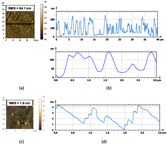
Figure 1. (a) AFM image of the surface of an unpolished R-cut sapphire substrate with the indicated rms roughness and (b) line profile of an unpolished sapphire substrate (up) and a detailed profile line for a length of 3 µm. (c) AFM image and rms roughness and (d) line profile of a thermally treated unpolished sapphire substrate where wide plateaus are detected.
Download figure:
Standard image High-resolution imageOn these unpolished substrates, the deposition of the CZO metalorganic precursor solution became inhomogeneous and achieving a continuous layer is very difficult. The growth of CZO buffer layers on top of these surfaces always led to the formation of some (111) CZO polycrystalline grains. Therefore, we conclude that the surface quality of unpolished sapphire substrates is not suitable for the growth of epitaxial CSDCZO buffer layers. Much smoother and therefore, plane surfaces are needed in order to achieve good quality and epitaxial CZO buffer layers. In order to improve the surface quality of the unpolished sapphire substrates, high temperature annealing treatments were performed expecting to induce planarization [33].
The unpolished sapphire substrates were thermally treated at 1100 °C and 1200 °C for 6 h and 2 h, respectively, in air atmosphere. As it can be seen in figures 1(c) and (d), the surface planarity has been greatly enhanced and the unit cell steps are visible. For comparison purposes, a line scan with a 3 µm length for an untreated sapphire substrate was introduced in figure 1(b). As it can be seen the outgrowths decrease from 150 nm to 4 and 5 nm in height. The unit step cells are detailed in figure 2. These plateaus are 600–700 nm long and exhibit a roughness of 1 nm or lower.

Figure 2. AFM profile line showing the unit step cells formed after a high temperature annealing of the unpolished sapphire substrates.
Download figure:
Standard image High-resolution imageOn these improved sapphire surfaces, the epitaxial growth of CZO buffer layers becomes feasible, but their surface quality is still poorly reproducible due to the inhomogeneity of unpolished sapphire substrates. Even though the planarity of the substrates surfaces has been strongly enhanced, there are still outgrowths present that can't be removed even with high temperature annealing. It has become quite clear then, that some type of polishing process is needed in order to achieve high quality surfaces, and so, comply with the requirements for a proper epitaxial growth of CZO buffer layers. However, a high quality polishing process is too expensive for the long length sapphire substrates (several meters) which are required for a SCFCL. Therefore, an intermediate quality polishing process, consisting of polishing the sapphire substrates just enough that the inhomogenities cannot be seen with an optical microscope, was tested. The surface of these BPS substrates is drastically improved as compared to unpolished ones, the planarity is greatly enhanced and the cost is extremely reduced, making them suitable for scalability. As it can be seen in figures 3(a) and (b), the remaining outgrowths are not higher than 5 nm, large flat areas are present and the planarity is higher than 70%. These surfaces are then apt for the deposition of highly epitaxial CZO buffer layers [33].

Figure 3. (a) Line profile showing large flat areas and small outgrowths and (b) planarity analysis showing more than 70% of flat area of a BPS substrate.
Download figure:
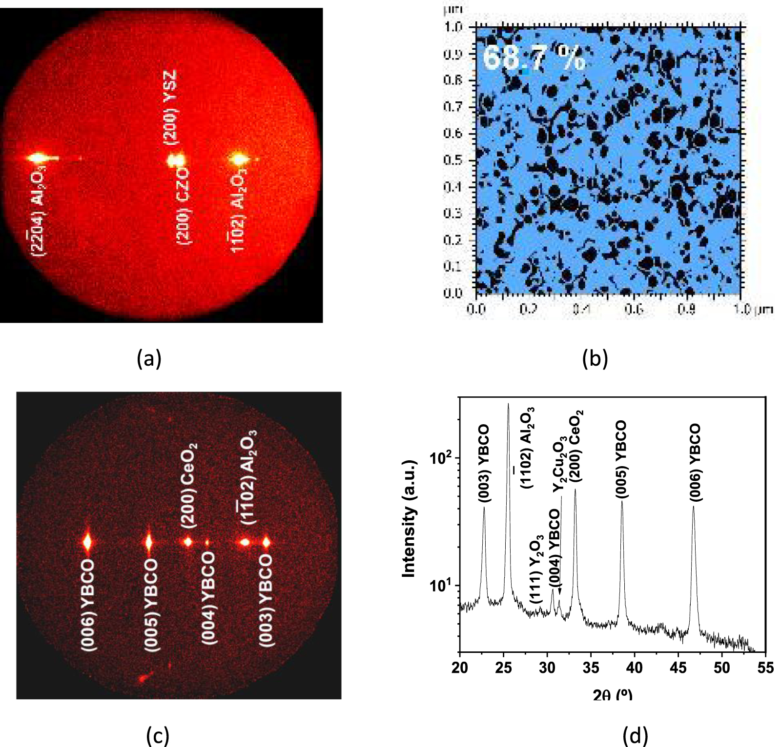
Standard image High-resolution imageIn the case of BPS substrates, epitaxial CSDCZO buffer layers could be easily achieved (figure 4(a)). The planarity percentage (figure 4(b)) is higher than 65%, complying with the requirements for the growth of epitaxial superconducting CSDYBCO layers (>60%) [32, 33]. The reproducibility in achieving this high planarity is higher than 75%.

Figure 4. (a) Two-dimensional GADDS image revealing a highly epitaxial CZO buffer layer grown onto YSZ/BPS and (b) planarity analysis of the CZO buffer layer confirming a high percentage of flat area; (c) 2D GADDS image of a 200 nm layer of YBCO/CZO/YSZ/epi polished sapphire that exhibits a high epitaxy with no trace of BaCeO3 (controlled reactivity) and (d) the corresponding integrated θ–2θ spectrum.
Download figure:
Standard image High-resolution image3.2. Growth and characterization of YBCO layers onto CZO/YSZ/sapphire substrates
Achieving epitaxial and flat surfaces for CSDCZO buffer layers enable a higher control of the reactivity between CeO2 and the intermediate BaF2 phase [21]. This reactivity leads to the formation of BaCeO3 at the interface which has a high lattice mismatch with YBCO. If this reactivity is not properly controlled, it will lead to the nucleation of misoriented YBCO grains which degrade the superconducting properties. In the case of CeO2/epi-polished sapphire substrates, as it can be observed in figure 4(c), when the CeO2 buffer layer exhibits a high planarity the reactivity is avoided in 200 nm thick YBCO films and it is controlled for higher film thicknesses. For those achievements, the use of Ba-deficient YBCO precursor solutions was very beneficial, since this type of metalorganic precursor solution leads to high performance YBCO layers, at lower growth temperatures than stoichiometric YBCO [37], thus allowing the nucleation of YBCO without the formation of BaCeO3 crystalline phase.
The next step is the deposition and growth of thick CSD YBCO layers on BPS. In previous works [21, 22], we have demonstrated 1 µm YBCO growth on single crystalline substrates (LaAlO3, SrTiO3, CeO2/YSZ). Being aware of the ease to generate microcracks during YBCO growth beyond a critical thickness dc and its dependence with microstructural features [13, 18, 38], we investigated whether microcracks are generated in substrates with different degrees of polishing. With this purpose, different thicknesses of YBCO layers have been grown on unpolished, epi-polished and BPS substrates. As shown in figures 5(a)–(c), independently of the polishing quality of the substrates, microcracks parallel to the {100} planes are formed. We also observe that the microcracks density increases with the thickness of the YBCO. As earlier mentioned, the calculated critical thickness of YBCO layers on sapphire, above which the layer will present microcracks was expected at about 300 nm. In particular, CSD-TFA growth has never surpassed YBCO thicknesses of 250 nm on sapphire without microcrack formation in the YBCO layer. In order to analyze in which stage the microcracks are formed, we have investigated the different steps of the growth process of 600 nm CSD YBCO films deposited onto CSDCZO/sputtYSZ/BPS substrates. The as-deposited 600 nm YBCO films are first subjected to the growth process without going through the oxygenation step. The surface morphology of the tetragonal YBCO films are then investigated by scanning electron microscopy (figures 6(a)–(e)).
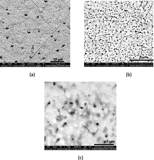
Figure 5. SEM image of the (a) 600 nm thick YBCO layers grown on epi-polished sapphire substrates, (b) 600 nm thick YBCO layers grown on unpolished sapphire substrates and (c) 200 nm thick YBCO layers grown onto BPS substrates. In all cases we can observe the formation of microcracks.
Download figure:
Standard image High-resolution image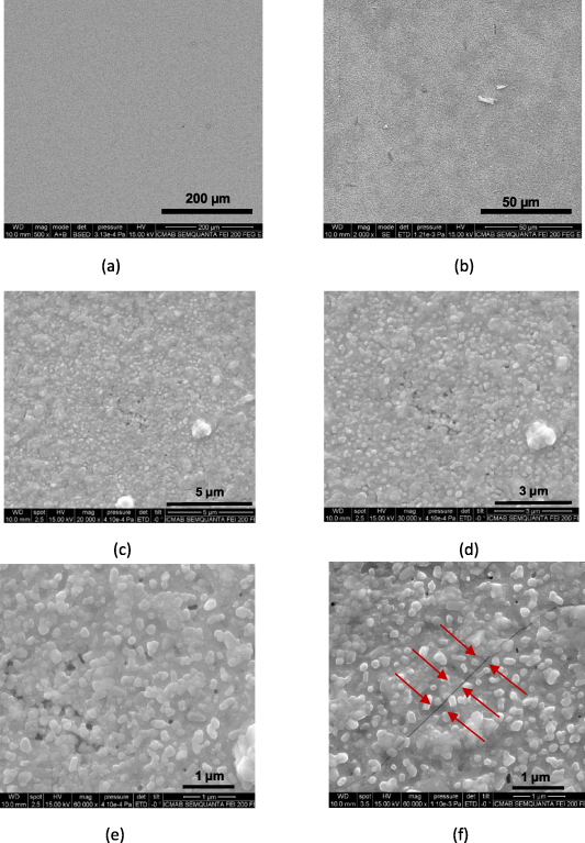
Figure 6. SEM images of 600 nm thick YBCO layers deposited and grown on CSDCZO/sputtYSZ/epi-polished sapphire before oxygenation (a)–(e) and after oxygenation (f).
Download figure:
Standard image High-resolution imageThese layers exhibit a low amount of porosity and surprisingly no presence of microcracks is revealed. So, even though the CSDYBCO layers thickness surpasses the critical thickness by a factor of 2, no microcracks are generated on the YBCO layer grown on BPS, confirming that they do not arise from the tetragonal phase. These YBCO layers are then subjected to a separate oxygenation process at 450 °C for 3.5 h (our standard oxygenation process). After this step, we indeed detect the presence of microcracks in the orthorhombic phase YBCO layers (figure 6(f)). Therefore, we conclude that the appearance of microcracks occurs during the transition from the tetragonal to the orthorhombic phase as a result of the change in in-plane lattice parameters.
With the aim of minimizing the risk of microcrack formation, we performed the oxygenation of the YBCO layers at a lower temperature (350 °C) to slow down oxygen diffusion and strain generation [39]. Longer periods of time were then required to achieve full oxygenation (more than 6 h). This approach was proved to be successful for layers up to 400 nm in thickness. As it is seen in figures 7(a) and (b), up to these thicknesses, we are able to achieve highly epitaxial and microcrack free YBCO layers. Keep in mind that 400 nm is higher than the calculated critical thickness (∼300 nm) of YBCO layers on sapphire substrates.
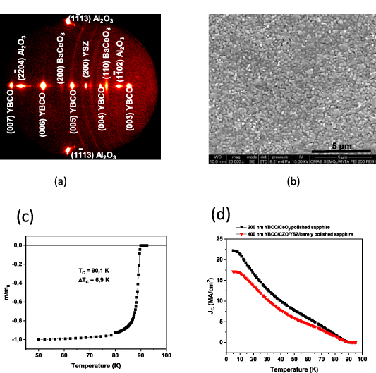
Figure 7. (a) Two-dimensional GADDS image revealing a highly epitaxial 400 nm thick CSDYBCO/CSDCZO/sputtYSZ/BPS, (b) SEM image showing a microcracks free layer, (c) SQUID measurement of the critical temperature TC and (d) JC dependence with temperature for a 200 nm YBCO film grown on epi-polished sapphire substrate (black) and for a 400 nm YBCO film grown on BPS.
Download figure:
Standard image High-resolution imageEven though we distinguish the presence of BaCeO3, (figure 7(a)) the reactivity between BaF2 and CeO2 did not have any effect on the YBCO texture. The 400 nm CSDYBCO layers exhibit a fairly low porosity (figure 7(b)), a self-field JC at 65 K of 3.7 MA cm−2 and at 77 K of 1.9 MA cm−2, as well as a sharp superconducting transition with an onset critical temperature TC = 90 K (figures 7(c) and (d)). The self-field total critical currents at 65 K and 77 K are then IC ∼ 150 A cm−1 w−1 and IC ∼ 80 A cm−1 w−1, respectively. These values are close to those achieved in YBCO films grown on epi-polished sapphire by vacuum deposition techniques or CSD [1, 16, 40, 41], and by CSD on CZO/YSZ-single crystal substrates for similar thicknesses [21].
Also, in figure 7(d) we show a moderate decrease of self-field Jc(T) in 400 nm thick films grown on BPS as compared to 200 nm ones on epi-polished sapphire substrates. The Ic values are already fairly promising in view of using these elements for SFCL applications [1], thus further understanding of the microstructure and strain generation mechanism is a very relevant issue to pave the way to increase the YBCO film thickness and prevent the generation of microcracks. We have, therefore, first investigated the epitaxial growth of YBCO on CSDCZO/sputtYSZ/BPS, through cross-sectional TEM observations (figure 8).

Figure 8. (a) Cross-sectional TEM image of YBCO/CZO/YSZ/BPS. Cross-sectional HRTEM images of (b) YSZ/sapphire interface, and (c) CZO/YSZ interface. Insets show the FFT pattern of YSZ/sapphire interface and CZO/YSZ interface, respectively. (d) Cross-sectional HR-TEM image of c-axis growth of YBCO. Inset shows the FFT pattern of YBCO/CZO interface corresponding to the orange square in figure (a), revealing the epitaxial growth of YBCO on CSZ.
Download figure:
Standard image High-resolution imageFigure 8(a) shows an intermediate magnification cross-sectional TEM image of the combined stack comprised of YBCO grown on 15 nm of CZO buffer layer/35 nm of YSZ on BPS substrate, as indicated. We can observe in HR-TEM image (figure 8(b)) that the CZO/YSZ interface is flat and free of secondary phases or other reaction, with clear boundaries between the CZO buffer layer and YSZ. FFT pattern in the inset in figure 8(b) shows that the buffer layer of CZO grown onto YSZ/BPS is epitaxial. HR-TEM image in figure 8(c) combined with the FFT pattern of YBCO/CZO interface (inset in figure 8(c)) reveals the epitaxial c-axis growth of YBCO film on CSDCZO/sputtYSZ/BPS, coinciding with the results observed in XRD data (figure 4).
We have then investigated the strain generation mechanism in the multilayer CSDYBCO/CSDCZO/sputtYSZ/BPS architecture to minimize the risk of microcrack formation when the film thicknesses are increased. To acquire this knowledge, we analyzed the cell parameter evolution at different steps of the growth process of all the layers in a 200 nm film of CSDYBCO/CSDCZO/sputtYSZ/BPS through RSM.
RSM were first performed for the CSDCZO/sputtYSZ/BPS system and the results are shown in figure 9. For the sputtered YSZ layers and for the CSDCZO buffer layers the calculated values for the in-plane cell parameters  were found to be
  = 0.5067 nm and
  = 0.5296 nm, respectively. When grown on sapphire substrates both of these layers become compressive (
 (YSZ) = −1.03% and
  (CZO) = −1.65%, where
  is the lattice mismatch, af
is the film in-plane parameter and ab
is the bulk parameter) with respect to the bulk values (abulk = 0.512 nm for YSZ and abulk = 0.5385 nm for CZO). The in-plane lattice misfit of CZO versus YSZ turns out to be compressive with
is the lattice mismatch, af
is the film in-plane parameter and ab
is the bulk parameter) with respect to the bulk values (abulk = 0.512 nm for YSZ and abulk = 0.5385 nm for CZO). The in-plane lattice misfit of CZO versus YSZ turns out to be compressive with  = −4.8%.

Figure 9. RSM for the CSDCZO/sputtYSZ/BPS films.
Download figure:
Standard image High-resolution imageWhen YBCO is grown on top of this buffered sapphire substrate the cell parameters for both YSZ and CZO are modified. This has been previously observed as well by Nie et al [38]. After the oxygenation of YBCO, the cell parameters of YSZ and CZO become  = 0.5106 nm and
  = 0.5429 nm, respectively. The compressive strain for YSZ becomes smaller (
 (YSZ) = −0.27%), but the growth of YBCO appears to induce a tensile strain to the CZO buffer layer (
 (CZO) = +0.81%), thus the misfit of CZO versus YSZ increases to
  = −6.4%. The RSM for the CSDCZO/sputtYSZ/BPS films after the growth and oxygenation of CSDYBCO is presented in figure 10(a), along with the RSM of the (308) and (038) reflection of YBCO (figure 10(b)).
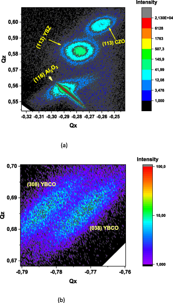
Figure 10. RSM (a) for the CSDCZO/sputtYSZ/BPS films after YBCO growth (left) and (b) for the orthorhombic YBCO grown on this system (right).
Download figure:
Standard image High-resolution imageCalculating the strain of YBCO with respect to the CZO buffer layer grown on BPS substrates we found that YBCO suffers a tensile strain in the  direction (
 = +0.28%) and a compressive strain in the
  direction (
 = −1.3%). These values were calculated with the
  = 0.3838 nm
  because the YBCO lattice is rotated 45° with respect to that of CZO.
In the case of non-oxygenated YBCO, the strain in both directions  is compressive with
  = −0.57% and
  = −2.13% (figure 11). Non-oxygenated YBCO (NOYBCO) seems then to be compressive with respect to the CZO buffer layers grown on BPS substrates. Therefore, no microcracks are generated during growth and cooling process under an oxygen pressure of 0.2 mbar which keeps a small orthorhombic distortion.

Figure 11. RSM for the NOYBCO/CSDCZO/sputtYSZ/BPS films.
Download figure:
Standard image High-resolution image
When the transition from the non-oxygenated phase to orthorhombic phase takes place, the oxygen doping leads to an increase of the  parameter generating a compressive strain along
  -direction, but to a decrease of
  lattice parameter which creates a tensile strain in the orthorhombic
  -direction. So, when oxygenating CSDYBCO/CSDCZO/sputtYSZ/BPS, YBCO is subjected to a tensile stress with respect to the CZO buffer layer in the in-plane
  -direction. Consequently, the microcracks are formed somewhere parallel to (100) crystallographic planes, although due to the twinned structure of YBCO, microcracks along the two in-plane orthogonal directions are observed (figure 5). As we have mentioned before, we could avoid the microcrack formation in films with thicknesses up to 400 nm by lowering the oxygenation temperature, which smoothens the kinetics of tensile strain generation. These results suggest that for higher film thicknesses further engineering of the interlayer strain generation is required in order to minimize the tensile stress in the
  direction.
In order to confirm our conclusion, we have performed RSM on a similar architecture without sapphire: CSDYBCO/CSDCZO/YSZ single crystal. We have found that in the case of this architecture, YBCO is compressive with respect to the CZO in both in-plane directions, in the non-oxygenated and fully oxygenated orthorhombic structure. In the case of the orthorhombic YBCO, the compressive strain along  and
and  directions were
  = −0.23% and
  = −2.07%, respectively. This is the reason that we do not observe microcracks when growing YBCO onto this architecture, even when 1 µm of thickness is achieved [21].
4. Summary and conclusions
Three different issues need to be addressed when growing YBCO onto CSDCZO/sputtYSZ/sapphire (unpolished and barely polished) system: the sapphire substrates surface quality, the reactivity between CZO buffer layers and YBCO, and last, but very important, the microcracks formation. For YBCO layers up to 400 nm in thickness, we have been successful in solving all these issues. The quality of sapphire substrates has been sufficiently improved with acceptable costs for long length by performing an intermediate quality polishing process. Regarding the reactivity between CZO and YBCO, we have proved that it depends on the quality of the CZO buffer layers. The use of Ba-deficiency solutions has helped to decrease the growth temperature and, consequently, the reactivity too. The formation of microcracks has been eliminated in films with thicknesses up to 400 nm by lowering the oxygenation temperature which then smooths the strain generated during the tetragonal-to-orthorhombic transition of YBCO, although the oxygenation time had to be considerably increased. In this case, we have achieved highly epitaxial layers, free of microcracks with good superconducting properties (JC(77K) ∼2MA cm−2).
We have seen that the main factor for microcrack generation is the tensile strain generated by the in-plane mismatch of YBCO and CZO when grown on sapphire substrates. We have found that microcracks appear parallel to the (100) planes during the tetragonal–orthorhombic transition, due to the decrease of the a-lattice parameter that generates a tensile strain from YBCO on to CZO along this direction. In order to overcome microcrack formation and be able to accommodate larger YBCO layer thicknesses onto the CSDCZO/sputtYSZ/BPS architecture, strain engineering of the CeO2 buffer layer lattice parameter through doping could be investigated to reduce the mismatch with the  lattice parameter of orthorhombic YBCO.
Acknowledgments
The authors acknowledge the funding of this research by FASTGRID Project (EU-H2020, 721019), the Projects COACHSUPENERGY (MAT2014-51778-C2-1-R), SUMATE (RTI2018-095853-BC21 and RTI2018-095853-B-C22) from the Spanish Ministry of Economy and Competitiveness which were cofunded by the European Regional Development Fund, the Project 2017-SGR 753 from Generalitat de Catalunya and the COST Action NANOCOHYBRI (CA16218). ICMAB authors also acknowledge the Center of Excellence Awards Severo Ochoa SEV-2015-0496 and CEX2019-000917-S. Authors acknowledge the Scientific Services at ICMAB and ICN2 Electron Microscopy Division. Authors acknowledge the use of instrumentation as well as the technical advice provided by the National Facility ELECMI ICTS, node 'Laboratorio de Microscopías Avanzadas' at University of Zaragoza.
Data availability statement
The data that support the findings of this study are available upon reasonable request from the authors.