
Abstract
In the past decades, low-dimensional semiconductors received intensive research interest. By introducing intentionally size-confined nanostructures or crystal imperfections, low-dimensional semiconductors have been broadly exploited as zero-dimensional quantum dots (QDs) for high-performance quantum emitters. The QD-based nonclassical light sources allow not only the deterministic generation of single photons but also entangled-photon pairs. However, the randomness in strain, shape and composition in semiconductors results in unpredictable transition energies for different QDs. This complication impedes the generation of single and entangled photons with well-defined energies, which fundamentally limits the success probability of scalable quantum information technologies. Strain engineering, a unique and powerful method to reshape the electronic states of semiconductors, has advanced the development of all-solid-state low-dimensional semiconductor based single and entangled-photon sources. In this review, the recent progress of employing mechanical strain field to control the electronic states and optical properties of low-dimensional semiconductors is reviewed. A comprehensive summary of diverse strain engineered devices for engineering the exciton binding energy, the coherent coupling of electronic states, the optical properties of low-dimensional semiconductors including single and entangled photons are provided. In addition, prospects and challenges of deploying the strain-engineering technique for future scalable quantum networks and photonic quantum circuits are discussed.
Export citation and abstract BibTeX RIS

Original content from this work may be used under the terms of the Creative Commons Attribution 4.0 license. Any further distribution of this work must maintain attribution to the author(s) and the title of the work, journal citation and DOI.
1. Introduction
Photons are natural carriers for information processing due to their extremely low transmission loss and high propagation speed. Analogous with electronics, the unique applications of photonics continue to emerge since the first laser light source was invented in 1960 s. Distinguishing from the black-body radiation, a laser can generate spatially coherent photons with super-high irradiance in a very tiny spot. These genuine features have boosted a wide range of photonic applications from everyday life to the most advanced science, e.g. telecommunications [1], biophotonics [2, 3], holography [4, 5], gravitational wave detection [6] among others. Nevertheless, photons emitted from lasers display Poisson statistics in a regular time interval, which gives rise to an unavoidable shot-noise in the photonics applications. In this regard exploring light with sub-Poissonian statistics to overcome the shot-noise in conventional photonic applications is particularly desirable [7].
A single mode of quantized light field, that is single photon, can be utilized as a flying photonic quantum bit (qubit) [8]. In contrast to the traditional binary bit that is either zero or one, photonic qubit can be in two states at the same time. This intriguing characteristic is known as quantum superposition [9], which forms the foundation of the modern quantum mechanics. Encoding information into photonic qubits that harness quantum superposition as well as other features like quantum entanglement would not only allow for the suppression of noise to improve the precision of measurement, but also enable photonic quantum technologies with novel functionalities that are impossible for classical light [10]. For instance, enhanced security could be achieved by encoding information into single photons or entangled-photon pairs such that an eavesdropper could be detected [11]. Carrying information with indistinguishable single photons enables unprecedented parallel computation power, i.e. quantum computer [12]. Moreover, recent years have witnessed tremendous success of applying single photons in ubiquitous quantum applications including remote quantum sensing [13, 14], quantum metrology [15], and quantum lithography [16, 17] and so on.
The ever-increasing importance of photonic quantum technologies exploiting the quantum properties of light requires suitable sources that are capable of generating single photons and entangled-photon pairs in a regulated stream [18, 19]. At the heart of the development of these nonclassical light sources lines the exploration of robust solid-state quantum emitters that are bright, deterministic, indistinguishable [20, 21] and indisputably compatible with a diode structure to realize electrical excitation. Thus far, the most widely used single and entangled-photon sources (SPSs and EPSs) are based on nonlinear process in optical media such as spontaneous parametric down-conversion and four-wave mixing [22, 23]. These nonlinear processes can create not only heralded single-photon state but also correlated photon pairs with quantum entanglement, for example, time-bin entanglement [24–26], polarization entanglement [27–29] and two-path entanglement [30] and so on. However, compared with the true quantum emitters, parametric-down conversion or four-wave mixing sources have manifold shortcomings in practical photonic quantum technologies. Just as the laser sources with Poisson statistics in the photon number, parametric down-conversion and four-wave mixing sources may generate zero or multiple photons. This probabilistic nature would cause bit errors in quantum algorithm protocols and thus fundamentally limit their usefulness in deterministic quantum technologies. Furthermore, this type of sources is not scalable as the probability of emitting single or entangled-photon states decreases exponentially with the number of sources [30].
Over the past decades, a variety of physical systems have been investigated for developing deterministic quantum light sources. Progress has been made in realizing single and entangled-photon emission from trapped atoms and ions [31, 32], and molecules [33–35]. However, atoms and trapped ions are in vapor phase and molecules are vulnerable to photo-induced chemical reactions, and thus they are not suitable for the practical photonic quantum applications, especially for on-chip quantum applications. Low-dimensional semiconductors such as quantum dots (QDs) are among the most promising sources of deterministic single photons and entangled photons owing to their atomic-like emission properties with high brightness and narrow spectral line width [18, 19]. Recent experiments have already demonstrated their suitability and feasibility for generating high degree of indistinguishable single photons. In particular, QD-based SPSs have been exploited successfully for high rate multi-photon boson sampling quantum applications which has proven to be impossible for conventional parametric down-conversion sources [36, 37]. Of the greatest interest is that the semiconducting QDs are solid-state materials and they allow for monolithic integration with photonic chip towards large-scale quantum photonic circuits [38–40]. From the practical device application point of view, semiconducting QDs can be easily embedded in a light-emitting diode (LED) in order to achieve electrically driven SPSs and EPSs [41–44]. This outstanding feature alleviates the use of complex and bulky laser system and therefore a full-fledged optoelectronic quantum network operated by macroscopically separated, QD-based quantum light sources can be expected in the near future. In addition, another major advantage of semiconducting QDs is the flexibility to incorporate them into various microcavities using in situ epitaxial growth and semiconductor processing techniques. For example, semiconducting QDs could be precisely embedded into photonic crystals [45, 46], microdisks [47–49] and Bragg grating cavities [50, 51] thereby their spontaneous emission rate, coherence as well as the collection efficiency can be steered in a controlled manner [52, 53]. To date, low-dimensional semiconducting QDs have contributed versatile solid-state quantum emitters for exploring photonic quantum technologies [36, 37, 54, 55].
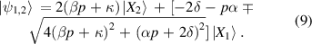
Strain engineering of the electronic and optical properties has long been pursued in low-dimensional semiconductors. Recent development of strain engineering has advanced the development of all-solid-state low-dimensional semiconductor based SPSs and EPSs with superior performance. It has been reported that the mechanical strain field can not only steer the emission energy of single-photon state from QDs [43, 56], but also control the coupling of the exciton states in QDs to enable entangled-photon emission [57]. Noticeably, the strain field with proper configurations can engineer both quantities so as to achieve entangled-photon emission with well-defined energies [58–61]. In recent years, exerting strain field to reshape electronic states of QDs has advanced rapid development of QD-based SPSs and EPSs, for instance, deterministic arrays of SPSs in atomically thin semicondutors, wavelength-tunable single-photon light-emitting diodes (SPLEDs) [43], entangled-photon light-emitting diodes (EPLEDs) [44, 62], scalable EPSs [58–61]. Strain-tunable QD-based light sources have emerged as one of the most practical nonclassical light sources for future large-scale quantum communication [63] and computation [64] tasks. The purpose of this letter is to review the recent progress of employing mechanical strain field to control the optical properties of QDs, including the binding energy, the coherent coupling of exciton states and both of them.
This review paper is constructed as follows. The basics of semiconducting quantum light sources is introduced in section 1, and then we discuss a generic theory on the strained semiconductor in section 2. In section 3, we present the significant research progress of employing strain fields to engineer the binding energy of low-dimensional self-assembled QD-based SPSs. Section 4 delves further into the deterministic creation of site-controlled QDs by applying nanoscale strain fields to atomically thin transition metal dichalcogenides (TMDs). In sections 5 and 6 we offer a comprehensive summary of diverse strain engineered self-assembled QD devices for achieving EPSs and scalable EPSs, respectively. We critically analyse the general relationship between the exciton energy, the polarization, and the coherent coupling of bright exciton states under external strain fields. Finally, the prospects of strain field based quantum engineering techniques including on-chip integration, nanostructured strain field engineering are discussed.
2. The coupling of low-dimensional semiconductors with external strain fields
Strain effects have been of great interest for low-dimensional semiconductors. It has been shown that the most important material properties like lattice constant, band gap and effective mass can be engineered in a controlled manner by external strain field. In order to understand the optical properties of the strained low-dimensional semicondtors, it is necessary to know the electronic band structures including the energy bands and the corresponding wave functions. When a stress is applied, the interatomic distance changes. Using the coordinate transformation, the lattice vector  where
where  ,
,  are the deformed lattice vector and undeformed lattice vector,
  is the strain tensor induced by the applied stress. When the deformation of the semiconductor is uniform and slow, the periodicity of the crystal lattice remains so that the Bloch theorem is still be applicable. In this scenario, the modification of the band structure for the semiconductor can be modelled by using the well-known Pikus-Bir Hamiltonian, based on the
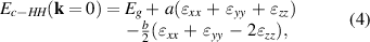
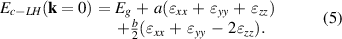
  method [65]. Considering the spin-off bands are generally several hundreds of meV below the heavy-hole (HH) and light-hole (LH) bands, the Pikus-Bir Hamiltonian dictates the change of the strain-induced conduction band and valence bands of GaAs at k = 0 as follows [66]:


where  ,
,  are the deformation potentials of the conduction band and the valence bands respectively,
  is the tetragonal deformation potential of the valence bands,
  is the mass of the free electron,
  is Luttinger parameter,
  ,
,  and
and  are strain tensor components. Set
  , which is the hydrostatic deformation potential, we obtain:
For typical semiconducting GaAs material, the related material parameters are:  ,
,  ,
,  . Given a biaxial strain applied to the GaAs,
  and
and  (where
  and
and  are elastic constants of bulk GaAs and
  and
and  ) [67]. As the strain is varied from compression (
 ) to tension (
 ), equation (1) suggests that the band edge decreases. In the meantime, the degeneracy of the valence bands is lifted, with LH and HH maxima decreasing and increasing, respectively. These behaviors are illustrated phenomenally in figure 1.

Figure 1. Strain-field-induced energy bands change for bulk GaAs in single particle picture. (a) Biaxial compressive strain ( ) removes the degeneracy of the HH and LH bands, and increases the band gap as compared to the unstrained band structure in (b). (c) Biaxial tensile strain field (
 ) decreases the band gap and for a sufficient tensile strain the LH band shifts above the HH band.
Download figure:
Standard image High-resolution image3. Strain engineered self-assembled QDs for SPSs
Self-assembled QDs are typical low-dimensional semiconductors, and they are man-made solid-state materials with typical size ranging from a few lattice constants to a few hundreds of nanometers. A representative example is the InGaAs QD in GaAs matrix by using the Stransky–Krastanov (SK) growth method [68, 69] (see figure 2(a)). The lattice mismatch between the InGaAs and the GaAs induces a smooth and nearly parabolic strain deformation potential. Meanwhile the combined effect of the band-edge discontinuity leads to a strong three-dimensional quantum confinement for carriers (electrons and holes) in the QDs. As a result, the electronic states of electrons and holes exhibit uniquely regular and atomic-like discrete energy levels. When photons with sufficient energy impinge the QDs, they can excite electron-hole (e-h) pairs composed of electrons with spin se,z = ±1/2 in the conduction band and holes with spin sh,z = ±3/2 in the valence bands [70]. Since these quasiparticles are charged, they interact with each other through the electrostatic Coulomb force which causes their motions to be correlated, forming a bound entity called the exciton. According to the angular momentum conservation, four exciton states could be formed, M = se ,z + sh ,z = ±1, ±2. M = ±1 are optically active states (the bright exciton), while M = ±2 are spin-selective prohibited, and are therefore optically inactive (the dark exciton). In addition, the exciton can trap additional electrons or holes, and single negatively or positively charged exciton could be formed. This charged exciton state is the mixture of spin-singlet and spin-triplet states [71], which has been testified as a promising spin platform for spintronics applications in which the long coherent electron/hole spin can be initialized, manipulated and read out by optical means [73]. Moreover, the charged exciton has been extensively investigated recently for developing heralded spin-photon entanglement [54, 74], which represents a remarkable progress to build a hybrid quantum interface involving 'stationary' qubits and 'flying' qubits simultaneously.

Figure 2. Structure of a single self-assembled QD and its basic optical properties. (a) Atomically resolved scanning tunneling microscopy image of a single InGaAs/GaAs QD. The image shows the height profile of a QD along the GaAs crystalline axis [110] and [1–10], respectively. A strong shape anisotropy along the two axes is clearly seen [72]. (b) Biexciton cascade of a single self-assembled InGaAs/GaAs QD. The general shape anisotropy of the QDs results in a spin splitting (the FSS) between the non-zero angular momentum of the excitons states. (c) Optical spectrum of a single InGaAs/GaAs QD which is addressed by using a typical confocal micro-photoluminescence (µ-PL) setup. The sharp emission lines account for the exciton (X) and the biexciton (XX) photon emissions, respectively. Originating from the spin splitting of the exciton states, the exciton and biexciton photon emissions have doublet emission lines that polarize along the GaAs [110] and [1–10] axes. (a) Reprinted from [72], with the permission of AIP Publishing.
Download figure:
Standard image High-resolution imageApart from the neutral and charged exciton states, a self-assembled QD can be populated by two e-h pairs forming a biexciton state [75] at appropriate excitation power. Of the greatest interest is that the radiative decay of the biexciton state plays a key role in generating correlated photons. This is like the cascade transitions in Calcium atom reported decades ago [76]. It should be noted that the radiative decay of the biexciton state consists of two consecutive steps (see figure 2(b)). First, a transition from the biexciton state to the exciton states takes place, and this gives rise to the emission of a single photon (XX) and leaves the remaining e-h pair on the bright exciton states. Second, the residual e-h pair recombines within its lifetime, resulting in the emission of the second photon (X) and leaving the QD in vacuum state. A typical optical spectrum of a single QD possessing the spin splitting of the exciton states is shown in figure 2(c). These two-level systems provided by the excitonic transitions in self-assembled QDs are commonly used on-demand sources for high-quality single photons.
Low-dimensional semiconducting self-assembled QD-based SPS was for the first time explored by P Michler et al in 2000 [19]. After that, self-assembled QDs have been the subject of intensive research and they have emerged as one of the most promising SPSs used for advanced quantum applications. Dislike natural atoms or ions with identical energy levels, a source's randomness in strain, shape and composition results in a random distribution of the QDs transition energies [77], and the photon emission energy from a self-assembled QD can be inhomogenously broadened as large as several tens meV [78]. This complication renders optical coupling between self-assembled QDs and microcavities inconvenient. Most importantly, the random distribution single-photon state emitted from distant QDs hampers quantum interference mediated by indistinguishable photons, and consequently impedes scalable quantum information processing that essentially requires photonic qubits initialized at the same energy. Scaling QD-based SPSs to large quantum optical system remains challenging, and therefore the reduction of the QD inhomogeneous energy broadening is highly desirable for the development of identical SPSs. Precise tuning of the emission energy for arbitrary self-assembled QDs has already become a basic requirement for the most envisioned quantum optics experiments such as two-photon interference between distant QDs [79, 80], microcavity mode coupling [81, 82], all-solid-state quantum memory interface [83–85] and so on.
3.1. Strain-field-induced binding energy tuning of QDs
By exerting external biaxial or uniaxial strain field, the binding energy of the exciton and biexciton states of self-assembled QDs can be engineered in a controlled manner, thus offering a viable method to tune the emission energy of the QD-based SPSs. Pioneering work on the strain-induced binding energy tuning of self-assembled QDs has been conducted by F Ding et al [86]. In their work, a nanomembrane containing self-assembled InGaAs QDs was processed by using standard photolithography, and then followed by transferring it onto a piezoelectric actuator, [Pb(Mg1/3Nb2/3)O3]0.72−[PbTiO3]0.28 (PMN-PT) [87], using a polymer assisted bonding technique. Figure 3(a) shows a sketch of such device. When a bias voltage is applied, an in-plane compressive or tensile biaxial strain field can be obtained on the PMN-PT actuator and it can be subsequently exerted to the InGaAs QDs embedded in the nanomembrane. With this method, exciton emission energy of the InGaAs QDs can be dynamically and reversely tuned in a broad range of about 10 meV without appreciable deterioration of the emission linewidth and intensity. More interestingly, the exciton and biexciton from a single QD show different tuning speeds, and this intriguing feature allows for a resonant tuning the emission of XX with respect to the emission energy of X. Empirical pseudopotential [88, 89] calculations found out that the different energy shifts of X and XX are mainly ascribed to the different changes in the binding energies of XX and X upon compression or tension. It is worth noting that strain-induced binding energy tuning is not only valid for commonly used InGaAs QDs grown by SK method, but also effective for droplet GaAs QDs. In 2011, S Kumar et al [90] demonstrated a strain-tunable quantum device for tuning the energy of photons emitted from GaAs QDs grown by droplet etching method [91]. Instead of using polymer as bonding adhesive, they improved the bonding interface between the PMN-PT actuator and QD-containing nanomembrane by applying gold-thermocompression bonding method [92, 93]. The use of a gold bonding interlayer under moderate temperatures and pressures results in a hermetic and tight bond which provides higher strain uniformity across the QD-containing nanomembrane as well as more robustness against the failure of polymer bonding, therefore overcoming the limited tuning reproducibility in the previous device configuration. Figure 3(d) shows the color-coded µ-PL spectrum of droplet GaAs QDs as a function of in-plane biaxial strain fields applied from the underneath PMN-PT actuator. Akin to the previous results, a compressive biaxial strain results in a blue shift of the emission wavelength of QDs and vice versa. A maximal tuning range of ∼10.5 meV can be achieved (see figure 3(d)) and most importantly, this large energy tuning range almost covers the whole range of the inhomogeneous broadening of the droplet GaAs QDs. Since the droplet GaAs QDs has single-photon emission energy close to the resonance of the D2 transition energy of rubidium atoms at 780.241 nm (the dash line in figure 3(d)), when combined with the strain-induced binding energy tuning technique, it is prospective to build a hybrid interface between the droplet GaAs QDs and rubidium atoms for slowing down single photons. Merging both systems could enable the storage of QD emission—an important step towards the implementation of solid-state quantum memories and quantum repeaters [94, 95].

Figure 3. Strain-field-induced binding energy tuning of QDs. (a) Sketch of the strain-tunable InGaAs/GaAs QD device. The inset shows a microscopic image of the nanomembrane. (b) Biexciton binding energy of InGaAs as a function of the applied strain field. (c) Sketch of the strain-tunable droplet GaAs QD device in which the QD-containing nanomembrane was integrated on PMN-PT actuator by using a gold-thermocompression bonding technique. (d) Color-coded µ-PL spectrum of GaAs QDs as a function of the in-plane strain  , the white dashed line indicates the D2 transition energy of rubidium atoms at 780.241 nm. (e) Schematic of the strain-tunable QD nanowire antenna. (f) Strain tuning the energies of different single InGaAs QD excitons in the nanowire antenna. Each QD in each nanowire antenna exhibits a different strain tuning slope. (a), (b) Reprinted (figure) with permission from [86], Copyright (2010) by the American Physical Society. (d) Reprinted from [90], with the permission of AIP Publishing. (e), (f) Reprinted (figure) with permission from [98], Copyright (2014) by the American Physical Society.
Download figure:
Standard image High-resolution imageIntegrating piezoelectric actuator with nanomembrane provides a facile way to engineer QD-based single-photon emission energy for both SK and droplet QDs. Noticeably this method can be further extended to other structure like the QD-containing nanowire. Indeed, nanowire plays an important role for tailoring far-field pattern of single-photon emission from QDs in order to improve the extraction efficiency of single photon from solid-state host material with higher refractive index [96, 97]. Due to the tapered waveguide structure, the nanowire containing self-assembled QDs has proven to be compatible with large spectral tuning range as the photons can be funneled in the nanowire with high confinement. Hence both high tunability and efficient quantum photonic devices can be envisioned at the same time when combining an external strain field tuning. Figure 3(e) shows such a QD-containing nanowire antenna device [98]. It was created by using the deterministic top-down fabrication procedure involving electron beam lithography and dry-etching processes. Reversible in situ binding energy tuning of the QD emission from the nanowire has been realized under the strain fields from the PMN-PT actuator. Figure 3(f) illustrates the exciton emission energy tuning from which a maximum tuning range of about 1.2 meV has been observed. In addition, the top gold on the PMN-PT actuator acts as not only the electronic contact for driving the piezoelectric actuator, but also terminates one end of the nanowire to reflect the generated single photons towards the out-coupling nanowire tip. As a result, a conical taper is introduced to confine the light mode into a plane wave in free space. Along with the accomplishment of the elastic tuning for the QD emission, high single-photon extraction efficiency above 50% has been simultaneously pursued. In addition to the top-down fabrication procedure, QD-containing nanowire can also be integrated onto the piezoelectric actuator by simply using 'pick up' and 'place' method. Y Chen et al [56] used this method and successfully laid InAsP QDs containning nanowire on the PMN-PT actuator. This configuration suffices strain transferring from the piezoelectric crystal to QDs and consequently the exciton energy of single InGaP QD in the nanowire is shifted by several meV without degrading the optical intensity and single-photon purity. Particularly, the 'pick up' and 'place' method facilitates integration of nanowire with extremely low loss silicon nitride waveguides which sits on the piezoelectric actuator [39]. This novel hybrid quantum photonic circuits combining III–V QDs, silicon nitride waveguides and piezoelectric crystals enable a new class of application towards realizing reconfigurable integrated quantum photonics, with full control over the quantum sources and the photon circuits.
Thus far, strain field has shown its powerful tuning capability to control the exciton binding energy and the exciton emission energy of the self-assembled QDs for SPS applications. Though all experimental works focus on the HH exciton ground states and the lower states, i.e. the LH states, are rarely studied due to the strong quantum confinement and large intrinsic compressive strain field in conventional InAs QDs. SPSs based on the LH ground exciton is appealing as it has been suggested to be more favorable for quantum information technologies. These include coherent state conversion between flying photonic qubits and stationary electron spin qubits [99, 100], faster and more stable control over the electron spin [101] and, most importantly, the LH photon emission has an additional out-of-plane polarization as compared to the HH exciton photon emission (see the right panel in figure 4(a)). These characteristics allow the LH single-photon emission to be initialized and manipulated much easier with respect to its HH counterpart. Despite the above advances, it was a long haul to pursue the LH exciton ground state in self-assembled QDs experimentally until the recent hallmark work on the creation of the LH exciton in droplet GaAs QDs by means of strain engineering. The strained band engineering already dictates that the HH and LH states can be inverted as a sufficient tensile strain is applied (see figure 1) [102]. Following up this theoretical prediction, Y H Huo et al [103] firstly grew unstrained droplet GaAs QDs in AlGaAs matrix in which conventional HH ground states are formed. To allow the LH states to be inverted and become the ground state, a biaxial tensile strain of about 0.36% is induced by embedding them into symmetrically pre-stressed In0.2Al0.4Ga0.4As membranes, which were released from the substrate after removing the sacrificial layer of AlAs. The QD heterostructure is shown in the left panel of figure 4(a). The right panel of figure 4(a) shows the neutral LH exciton configuration consisting of the three bright states with in-plane and out-of-plane polarization components respectively. The nature of the LH exciton formation in this strained GaAs QDs is testified by using the confocal µ-PL measurement. Figure 4(b) shows a typical spectrum from a single GaAs QD with the LH exciton ground state, which is collected from the cleaved edge of the substrate. Unlike the HH exciton photon emission with only one polarization component, two polarization components have been unambiguously observed for the LH exciton emission. The simultaneous µ-PL measurement from the top of the QDs has also verified similar two polarization components (not shown), indicative of the LH exciton photon emission from QDs. The further anti-bunching has been taken and it clearly reveals single-photon emission nature of the tensile strained GaAs QDs [104].

Figure 4. Strained self-assembled QD for the creation of LH ground exciton states. (a) Stressed heterostructure of the QD-containing nanomembrane and neutral LH exciton consisting of three bright states and a dark state decaying to the ground state. (b) µ-PL spectrum of the LH exciton emission where the hollow squares and stars correspond to light polarized along the cleaved edge and the growth direction of the strained QD, respectively. (a), (b) Reprinted by permission from Springer Nature Customer Service Centre GmbH: [Nature] [Nature Physics] [[103] A light-hole exciton in a quantum dot Huo Y, Witek B, Kumar S, Cardenas J, Zhang J, Akopian N, Singh R, Zallo E, Grifone R and Kriegner D Nat. Phys. 2014, 10, 46].
Download figure:
Standard image High-resolution image3.2. Wavelength-tunable SPLEDs under strain fields
Strain engineering technique can be applied to self-assembled QDs that are embedded in LED heterostructures so as to demonstrate SPLED with wavelength tunability. For practical quantum applications, the electrically pumped SPLED is arguably favorable as compared to optically excited QD devices that generally require a large volume and high complexity. SPLED allows for demonstration of miniaturized solid-state devices and thus ensures an envisioned full-fledged optoelectronic quantum network operated by macroscopically separated, QD-based quantum light sources. The strain-tunable SPLED was firstly proposed and reported by R Trotta et al [92]. The demonstrated device consists of InGaAs QD-containing p-i-n diode nanomembrane integrated onto a 300 µm thick biaxial PMN-PT actuator by using thermal compression bonding technique (figure 5(a)). The gold interlayer acts as a common ground for the diode and the actuator, thereby electric bias can be applied without any crosstalk. The dc voltage Vd is applied for electronic carrier injection to InGaAs QDs embedded in the GaAs p-i-n diode while Vp is applied at the same time for driving the piezo-actuator. Figure 5(b) shows the micro-electroluminescence(µ-EL) spectra from a single InGaAs QD, from which a broad exciton tuning range of about 20 meV has been observed. This capability can be further utilized to randomly chosen QDs and their emission energies can be engineered to be specifically resonant with the desired frequency as shown in figure 5(c). This function would pave the way towards two-photon quantum interference between two electrically driven SPLEDs. Based on the similar device structure, the ultrafast pulse excitation technique was introduced later in order for realization of ultrafast and wavelength-tunable SPLED device [43]. Figure 5(d) shows the fast pulse excitation scheme in which a stream of fast voltage pulses synthesized with a dc bias was used to pump the SPLED. The purpose to apply the dc voltage is to compensate for the built-in potential of the diode (∼2 V) so that the high frequency electric pulses can be fed to QDs. The µ-EL spectra from electrically triggered QDs under different magnitudes of the dc bias are shown in figure 5(e). A total energy shift of 4.8 meV was achieved when the electric field from −10 to 20 kV cm−1 was applied. Another outstanding feature of the device is that implementing the repetition rate of the electric pulses enables the demonstration of a high-speed single-photon emission up to 0.8 GHz from this special strain-tunable quantum LED (as shown in figure 5(f)).

Figure 5. Strain-tunable SPLED. (a) Sketch of the SPLED integrated onto the PMN-PT actuator. (b) µ-EL spectra from a dc electrically driven and wavelength tunable QD as a function of electric field applied to the PMN-PT. (c) Emission energies from two independent QDs are tuned into the resonant energy. (d) Electrically pulsed excitation scheme and µ-EL spectra from a single InGaAs QD under electrical pulses excitation. (e) Strain-dependent µ-EL spectra from a strain-tunable SPLED under electrically pulsed excitation. (f) Autocorrelation measurement result at a high excitation repetition rate of 0.8 GHz. (a)–(c) [92] John Wiley & Sons. [Copyright © 2012 WILEY-VCH Verlag GmbH & Co. KGaA, Weinheim]. (d)–(f) Reprinted with permission from [43]. Copyright (2013) American Chemical Society.
Download figure:
Standard image High-resolution imageAside from the strain-tunable SPLEDs that contain mature InGaAs QDs, there is a strong motivation to implement ultra-compact electrically driven SPSs that based on droplet GaAs QDs. The reason is that they emit single photons whose energy is compatible with the D2 transition line of rubidium atoms [105]. In 2017, a strain-tunable and electrically pumped SPLED devices based on droplet GaAs QDs was demonstrated for the first time [106]. Figure 6(a) depicts the principle of slowing down deterministic single photons emitted from the electrically driven GaAs QD LED that couples to rubidium atoms. A voltage is applied to the PMN-PT so that the emission wavelength can be well controlled by the strain. By inserting a rubidium gas cell in the optical path, deterministic single photons emitted from electrically triggered GaAs QDs can be absorbed and then slowed down when the energy of photons is tuned to the D2 transition line (see figure 6(b)). The second-order autocorrelation function g(2)(τ) measurements of photons emitted from a bright QD have confirmed this slowing down regime as shown in figure 6(c). The blue line implies that the minimum of the g(2)(τ) will be delayed by a few nanoseconds when the emission wavelength is tuned into resonance with the rubidium D2 lines compared with the black line.

Figure 6. Strain-tunable SPLED interfacing with rubidium atomic transitions. (a) Artistic picture of hybrid interface between the droplet GaAs QDs and rubidium atoms for slowing down deterministic single photons. (b) Color-coded µ-EL spectra under biaxial strain tuning. The circle indicates the absorption of rubidium atoms when emission wavelength of a droplet GaAs QD is tuned to be in resonance with the rubidium D2 transitions line 780.241 nm. (c) Anti-bunching measurements for the EL emission from a strain-tunable SPLED including droplet GaAs QDs. Upper panel shows the anti-bunching behavior when the GaAs QDs are energetically off-resonance with the rubidium D2 transitions line. Lower panel shows anti-bunching curve when the photons are tuned energetically into resonance with the rubidium D2 transitions line. (a)–(c) Reproduced from [106]. CC BY 4.0.
Download figure:
Standard image High-resolution image3.3. Strain tuning of self-assembled QDs coupled to optical microcavities
The piezoelectric actuator comprises a versatile platform for applying strain field to engineer QD optics in various nanostructures like nanomembranes, nanowire antennas, III–V compound heterostructures etc Apart from the above structures, applying external strain fields to QDs embedded in microcavities is promising to exploit quantum electrodynamics for tailoring single-photon emission properties which enables a robust way to create high-quality SPSs with high brightness and indistinguishability [107, 108]. Nevertheless, due to the random distribution of the QD transition energies, deterministic coupling of QD emission and the cavity mode remains a big challenge. Therefore, there is a strong demand for photon energy tuning. Strain tuning has shown great potential for tuning QDs as it can reversibly shift the photon emission energy with negligible effects on their emission linewidth and intensity as compared to other techniques. In 2013, S Sun et al [109] demonstrated a strain tuning of a QD strongly coupled to a photonic crystal cavity. Since the position of self-assembled QDs are completely random, the coupling between a single QD and a microcavity was ensured by using QD sample with relatively high density (10 ∼ 50 µm−2). Figure 7(a) shows an experimentally fabricated photonic crystal slab with 'L3' microcavity whose resonant properties were investigated in a normal confocal µ-PL measurement. It reveals that the Q value of the cavity for the demonstrated device is as high as 12 000, corresponding to a cavity decay rate of  (figure 7(c)). Figure 7(b) shows a schematic of the sample mount used to perform strain tuning, a L-shaped copper holder was mounted on the cold finger in a helium flow cryostat. The self-assembled QD sample and a PMN-PT crystal were fixed in parallel on the holder with the direction of the applied stress aligned along the row defect of the photonic crystal cavities. The PMN-PT substrate was poled in the [011] direction such that an out-of-plane electric field induced an anisotropic in-plane strain in the substrate. When the strain field was dynamically applied, it was clearly seen that the emission energy of QDs can be tuned at a relatively faster speed. Anti-crossing of the QD emission energy with respect to the cavity resonance was successfully achieved when the exciton energy was tuned through the cavity resonance at the applied electric field of 7.8 kV cm−1 as seen in figure 7(d). This provides an ambiguous signature of strong coupling between the self-assembled QD and the photonic crystal cavity with a coupling strength (g) of g/2π = 11.5 GHz.

Figure 7. Strain engineering self-assembled QD emission coupled with optical microcavities. (a) Scanning electron microscope (SEM) image of a photonic crystal cavity with 'L3' defect cavity. (b) Sketch of the experimental setup and sample configuration used to apply strain to the QD sample within a 'L3' photonic crystal slab cavity. (c) µ-PL spectrum of a photonic crystal cavity at low temperature. (d) Color-coded µ-PL spectra of QD emission and the resonant mode of photonic crystal cavity as a function of electric field applied on the PMN-PT actuator. (e) Sketch of the QD-containing and strain-tunable micropillar. (f) µ-PL spectrum of a QD-containing micropillar cavity. (g) Color-coded µ-PL spectra map of the micropillar cavity. (h) PL decay time as a function of QD-cavity detuning energies. Black points are measured at 4.5 K with different piezovoltages, blue and red points are measured at 6.5 K and 8 K, respectively. (a)–(d) Reprinted from [109], with the permission of AIP Publishing. (e)–(h) Reprinted with permission from [115]. Copyright (2019) American Chemical Society.
Download figure:
Standard image High-resolution imageStrain tuning of a QD strongly coupled to a photonic crystal cavity has provided a testing ground for studying quantum electrodynamics in solid-state devices, which plays a vital important role in nonlinear optical effects at a single-photon level such as single-photon all-optical switches [110, 111], cavity reflectivity controls [112] and photonic quantum logic operations [113, 114] and so on. As compared to the strong coupling, strain tuning a single QD and microcavity in the weak coupling regime allows for tailoring the radiation pattern of the QD emission, thereby enhancing the brightness of QD emission. In this context, strain-based external tuning can be implemented on a micropillar cavity with self-assembled QDs. Such optomechanical system combining the advantages of a micropillar resonator and the piezo-strain-tuning technique thus enables the deterministic single-photon emission enhancement via the known Purcell effect [115, 116]. The strain-based QD-containing micropillar device is schematically shown in figure 7(e). The sample was fabricated by using polymer assisted bonding technique in which a 30 µm thick GaAs nanomembrane consisting of a distributed Bragg reflector was bonded onto a 300 µm thick PMN-PT actuator. Thereafter, high resolution electron beam lithography and reactive ion etching processes were used to define the micropillars. The µ-PL spectrum in figure 7(f) shows several peaks where the narrow ones are emitted from the exciton emission of a single InGaAs QD and the broader is from the fundamental cavity mode. It is clearly observed that the emission lines are energetically off-resonance with the cavity in their initial state. By applying a positive (negative) voltage to the PMN-PT actuator, an in-plane compression (expansion) was induced in the substrate which can be transferred to the QDs embedded in the micropillars. Figure 7(g) gives the color-coded µ-PL spectra indicating that the QD transition line can be precisely tuned to be in resonant with the cavity mode. On account of the pronounced Purcell effect, a strong enhancement of the single-photon flux was observed. In the meantime, drastic supersession of the radiative lifetime of the single-photon emission has been found as the external strain field brought energy of photons to the resonance of the microcavity. It has been shown the Purcell enhancement factor can be up to 4.7 in this optomechanical quantum system.
4. Strain-induced arrays of SPSs in atomically thin two-dimensional semiconductors
There have been more than 60 types of TMDs reported so far, and among them molybdenum disulphide (MoS2), tungsten disulphide (WS2), tungsten diselenide (WSe2) and molybdenum diselenide (MoSe2) are well studied semiconducting compounds [117, 118]. They are made from group VI-B elements with structural formula of MX2, where M represents the transition metal atom and X denotes to the chalcogen atom. Figure 8(a) shows their crystal lattice structure in which the transition metal atoms are arranged in a triangular lattice and each of them is bonded covalently to six X atoms. In contrast to the gapless graphene material, these TMDs have direct band gap when thinned down to a single monolayer (ML). The band extrema are located at the high symmetric K points of the hexagonal Brillouin zone, which gives rise to the interband transitions in a broad spectral range (see figure 8(b)). The presence of a direct gap in group VI-B TMDs make them particularly appealing for potential photonic device applications because of the high efficiency for light emission. Moreover, ML TMDs are unique low-dimensional semiconductors as compared to the III–V semiconductors like InGaAs and GaAs QDs. They exhibit valley-selective optical transitions and non-zero Berry curvatures [119, 120], and thus the excitons in TMDs are spin-locked with respect to the valley degree of freedom. Meanwhile, ML TMDs possess strong two-dimensional (2D) confinement, thus the excitons have large binding energy up to a few hundreds meV and allow for stable photon emission at even room temperature. In addition, the flexibility of transferring and stacking super clean and different MLs into heterostructures [118, 121, 122] makes the TMDs suitable for solid-state quantum emitters in photonic quantum applications.

Figure 8. Basic structural and optical properties of the ML TMDs. (a) Typical crystal lattice structure of TMDs. (b) Direct band gap features of the ML TMDs when the TMDs are thinned down to the limit of the ML. Δsoc indicates the spin-orbit splitting in the ML. (c) Semicondutor-monolayer heterostructure in which a single layer of WSe2 was exfoliated and transferred onto an epitaxially grown GaInP/GaAs substrate. The white line indicates the scale bar of 5 µm and the bright spots mark the potentially localized light emitters. (d) PL spectra of the localized emitter in the ML WSe2 at 4.5 K for different excitation powers. (a), (b) Reprinted (figure) with permission from [117], Copyright (2018) by the American Physical Society. (c), (d) Reproduced from [123]. CC BY 4.0.
Download figure:
Standard image High-resolution imageRecent works have already shown that ML TMDs can contain crystal structural imperfections that refer to as QDs in TMD MLs [124–127]. These impurity defects are particularly interesting as they can act as zero-dimensional anharmonic quantum emitters. Until now, deterministic generation of single photons have been successfully realized in ML WSe2 and WS2/WSe2 heterostructures [125–130]. Interestingly, by transferring the ML WSe2 onto the epitaxially grown GaInP/GaAs substrate, He et al observed both exciton (p2 in figure 8(d)) and biexciton photon emission (p1 in figure 8(d)) from the randomly formed defects in the ML WSe2 (see the bright spots in figure 8(c)) [123]. Most importantly, the characteristic emission cascade is unambiguously verified in a cross-correlation experiment, and this sequential emission, a prominent example of the biexciton–exciton cascade, is a distinct feature of the semiconducting QDs that are likely to have very favourable properties for applications in quantum information processing.
Despite the remarkable findings of low-dimensional semiconducting QDs in TMDs for solid-state SPSs, the generation of these QDs has been reliant on their random occurrence. Deterministic creation of precisely positioned QDs in TMDs is important for the further investigation of this new class of QDs, as well as exploring them for scalable on-chip quantum applications. Since the origin of the QDs in TMDs arise most likely from the crystal imperfections or defects, applying strain engineering can circumvent the above challenge. Recently, two research groups proposed a promising nanoscale strain engineering technique to deterministically fabricate a 2D lattice of quantum emitters in the ML WSe2 [131, 132]. In their works, an all-dry viscoelastic stamp transferring technique was used to pick up and place the exfoliated ML WSe2 flakes onto a substrate with dielectric nanopillars fabricated by electron beam lithography and reactive ion etching. Figure 9(b) shows the processing flow for this unique nanoscale strain engineering technique. The nanopillars can be patterned on the silica/Si substrate with different heights ranging from 60 to 190 nm, as shown in the cross-sectional profile in figure 9(c). Owing to van der Waals force, a 2D flake conforms to the contours of a lithographically patterned nanopillar lattice, thus the point-like elastic biaxial strain can be created at the nanopillar lattice point, which leads to the localized excitons with quantized energy levels. With this method, the strain-tunable quantum emitters at the nanopillar locations have been demonstrated. Figures 9(d) and (e) show the color-coded spatial PL map from the nanopillar locations in the ML WSe2. The PL peaks distribute in a range of 740 to 800 nm, which is longer than the emission wavelength of the 2D valley exciton of the ML WSe2 (see figure 9(f)). The emission intensity collected from the locations of the nanopillars significantly increases by 10 ∼ 50 times as compared to the surrounding area without nanopillar structures. The emission line widths were observed as narrow as ∼180 µeV, which agrees with the previous report of the defect-based QD emission in the ML WSe2. The quantum nature of the photon emission was investigated by measuring the photon autocorrelation function g(2)(τ) as shown in figure 9(g). The obtained g(2)(0) values are obviously lower than the classical limit of 0.5, which provides clear evidence of the single-photon emission from these strain tuned nanopillar-based quantum emitters. We should note that the nanoscale strain engineering technique developed in the above works enables the deterministic creation of low-dimensional QDs in a large-scale exfoliated TMDs with the quantum confinement of the excitons. This strain tuning method by means of patterned nanostructures may open a way towards the placement of quantum emitters in photonic structures such as optical waveguides and microcavities where the precise and accurate positioning is highly desired [133].

Figure 9. Nanoscale strain-induced arrays of quantum emitters in the ML WSe2. (a) SEM image of the nanopillars. (b) Processing flow of transferring an exfoliated ML WSe2 onto a patterned silica nanopillars lattice. (c) Atomic force microscopy scan of the transferred ML WSe2 on one single nanopillar. The bottom panel shows the cross-sectional profile of the transferred structure. (d) Color-coded spatial PL map of the ML on the site-controlled nanopillars. The bright spots are the enhanced light emissions from the localized excitons in the ML WSe2. (e) Zoomed-in optical image of the fluorescent light emitting spots at the locations of the nanopillars. (f) Corresponding spectra of the localized excitons from the positions marked with the green cross symbols in (e). (g) Normalized photon correlations of the selected emission peaks in (f). (a)–(g) Reproduced from [131]. CC BY 4.0.
Download figure:
Standard image High-resolution image5. Strain engineered self-assembled QDs for high performance EPSs
Thus far, we have introduced the critical strain engineering techniques for the applications of solid-state SPSs based on epitaxially grown semiconductors and TMDs. In the next, we will focus on the strain-induced tuning effects for applications in EPSs. For epitaxially grown self-assembled QDs, it is worth noticing when the two intermediate bright exciton states are degenerate, the biexciton cascade can generate polarization-entangled photon pairs with two-photon quantum-mechanical state can be expressed with the Bell state  (H and V denote the orthogonally horizontal and vertical polarization) [41, 77, 134–136]. Since the discovery of the biexciton cascade for generating polarization-entangled photon emission [134], a new era was inaugurated for exploiting all-solid-state and deterministic EPSs in order to circumvent the probabilistic characteristic of the conventional parametric down-conversion sources. Strain engineering has been not only rapidly developed into the exciting research area that encompasses binding energy tuning and cavity coupling, but it has also sparked immense interest in the generation of deterministic entangled-photon pairs. In an ideal QD, the two bright exciton states are energy degenerate and the biexciton cascade provides no 'which path' information so that a polarization-entangled photon pair is emitted. The generation of the polarization-entangled photon pairs from such solid-state semiconducting materials has opened a new paradigm for nanoscale quantum device applications towards the future large-sale on-chip quantum photonic circuits with unprecedented brightness and flexibility. However, a realistic self-assembled QD possesses a random epitaxial growth procedure in which anisotropic exchange interaction leads to the energetic splitting of the two bright exciton states, the so called fine-structure splitting (FSS) [57, 62, 137]. This detrimental FSS leads to a phase evolution of the intermediate exciton states, and subsequently results in a transition of the biexciton-exciton photon pair from the expected polarization entanglement to only classical correlation. Theoretical and experimental studies have revealed that photon polarizations are only classically correlated rather than entangled unless the FSS is tuned well below the homogenous broadening of the exciton state (∼1 µeV) [138]. Up to now, tremendous progress has been made to study and manipulate the FSS of the self-assembled QDs and a number of in situ and post-growth tuning techniques have been developed to control it in order to demonstrate EPSs with strong polarization entanglement. These methods include rapid thermal annealing [53, 139], optical Stark effect [140, 141], in-plane magnetic field [135, 142], electric field [138, 143], strain field [43, 44, 61] and so on. In situ thermal annealing could enable a broad energy tuning of the exciton state by changing the potential profile of QDs. But this method is commonly a coarse tuning and it strongly relies on the precise control of the time and temperature used in the annealing process. Optical Stark effect is an alternative method to tune the QD exciton energy as well as its FSS. With this method, a strong continuous-wave laser with detuned frequency could create a pair of dressed exciton states, and it is always possible to find a detuning frequency to make the FSS vanish. However, using optical Stark effect to tailor the optical properties of QDs requires an additional laser for excitation, which makes the practical implementation difficult. Aside from the above methods, magnetic field can also tune the optical properties of QDs by mixing the dark exciton states and bright exciton states. It is worthwhile that the magnetic field was utilized to realize for the first time polarization-entangled photon emission from a self-assembled QD without any post-spectral filtering [41]. Arguably, it is practical to apply electric field to control the optical properties of QDs by using either lateral or vertical quantum-confined Stark effect [144]. This process, however, leads to a reduction in the optical intensity due to electric-field-induced reduction in e-h overlap. Moreover, it is hard to combine it with electrical excitation any more once the electric field is used as a 'tuning knob'. By contrast, strain engineering, a powerful method to manipulate the FSS of self-assembled QDs, has advanced the development of QD EPSs with superior performance. In 2006, Seidl et al [145] pointed out the possibility of reducing the FSS of self-assembled QDs by using uniaxial stress and the pioneering works showed a remarkable reduction of the FSS from 30 µeV to 15 µeV within the range of the applied stress. Exerting strain field to self-assembled QDs has now become an important technique for manipulating the FSS, and it has stimulated a rapid development of the QD-based EPSs with superior performance, for instance, entangled-photon emitting diodes and scalable EPSs. Strain-tunable QD-based EPSs have emerged as one of the most practical nonclassical light sources for future large-scale quantum communication and computation tasks.
5.1. Atomic model for strain engineering the FSS of self-assembled QDs
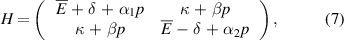
Let us consider a microscopic theory for strain engineering of the FSS for self-assembled QDs. Here we take the generic InGaAs/GaAs QDs for an example. For pure lens-shaped InAs QDs whose base is elongated along the GaAs crystal axis [110] or [1–10] direction, the point group theory predicts that the two bright exciton states belong to two different irreducible representations Γ2 and Γ4. It is noticed that the symmetry will be reduced to a lower value, that is C2 or C1, once the QD is elongated along the [100] ([010]) direction, or alloyed with gallium. In both cases, the two bright exciton states belong to the irreducible representation Γ1. Within the framework of the symmetry arguments, Singh and Bester concluded that the two exciton states with different irreducible representations could cross each other under an uniaxial stress along the [110] direction [137]. This means that the energy degeneracy between them can be removed and the FSS can be tuned exactly to zero. In contrast, for alloy InGaAs QDs with lower symmetry, anti-crossing takes place between the two bright exciton states, and thus there will be a lower bound for the FSS as seen in figure 10(d). It should be noted that a more generic theory on the strain engineering of the FSS of the self-assembled QDs was developed by Gong et al [57] in 2011. Most of the conclusions that we introduce here are taken from their paper. Let us first consider a generic self-assembled QD under an uniaxial stress and its Hamiltonian is given by


Figure 10. Atomic model and numerical calculation for strain cancelation of the FSS of QD. (a) Splitting between two bright states results in FSS for asymmetry QDs. (b) Polarizations of emission lines for different symmetries. (c) Crossing and (d) anti-crossing of the two bright exciton states under uniaxial stress along the [110] direction for pure lens shape InAs QD with C2
v
symmetry and alloy InGaAs QD with C1 symmetry respectively. The inset in (d) shows the strain-induced rotation of the polarization of the lowest exciton state. FSS as a function of stress for (e)  and (f)
  . (g) FSS and (h) polarization angle as a function of external stress, respectively. (b), (e)–(h) Reprinted (figure) with permission from [57], Copyright (2011) by the American Physical Society. (c), (d) Reprinted (figure) with permission from [137], Copyright (2010) by the American Physical Society.
Download figure:
Standard image High-resolution imagewhere n is the direction of the applied uniaxial stress and p is the magnitude of the stress. H2
v
accounts for the Hamiltonian of QDs with C2
v
symmetry. V1 is denoted as potential which reduces the symmetry to C1 and Vs
(n)p is the potential change arising from the external stress. By neglecting the spin-orbit interaction, the simplified Hamiltonian involving only the bright exciton states i.e.
 and
and  can be written as
where  ,
,  ,
, 
 ,
,  and
and  . Diagonalization of the Hamiltonian yields the following eigenvalues and eigenvectors:
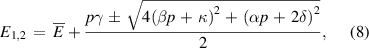
The energy difference  refers to as the FSS which can be expressed as
  with
with  and
and  . This formula implies that a lower bound corresponding to the minimum value of s can be obtained as
  at a critical value of the uniaxial stress
  . Regarding the eigenvectors,
  is the superposition of the two states
  and
and  . Indeed, they are two eigenvectors of H2
v
and their polarizations are aligned along the crystalline axis [110] and [1–10] respectively. As a result,
. Indeed, they are two eigenvectors of H2
v
and their polarizations are aligned along the crystalline axis [110] and [1–10] respectively. As a result,  indicates a polarization angle (
 ) of the new eigenvector with respect to the [110] ([1–10]) axis and it is quantified as
With the above theoretical analysis, it reveals that the values of  ,
,  ,
,  , and
, and  uniquely determine the FSS and the polarization angle. Especially, there are two special cases needed to be noted. First, when the direction of the applied uniaxial stress is along the [110] (or [1–10]) axis, the symmetry of the QDs will not change and thus anti-diagonal components of the perturbed Hamiltonian should keep constant no matter how large the stress is applied. In this case
  and the lower bound is found to be s = 2
 at p = −2
 as seen in figure 10(e). Secondly, when the stress is exerted along the [100] (or [010]) direction, the symmetry analysis yields
  , which results in the lower bound of s = 2
 at p = −
 as seen in figure 10(f). For both cases the lower bound of the FSS is only determined by the values of δ and κ. Further analysis unveils that δ and κ are material related parameters, and they can be expressed in terms of the FSS (s0) and the polarization angle (
 ) at p = 0:
  = −s0sin(2
 )/2 and
  = s0cos(2
 )/2. The above analytical analysis was further confirmed in the numerical calculation by using an empirical pseudopotential method. Figures 10(g) and (h) show the main calculation results for pure InAs/GaAs QDs with C2
v
symmetry. When the uniaxial stress is applied along the crystalline [110] ([1–10]) direction (black square), the FSS can be drastically tuned and it can be completely eliminated at a critical stress, which is in agreement with the analytical analysis. In the meantime, the polarization angle keeps almost constant as the applied stress is far away from the critical value, but it undergoes a dramatic change from 90º to 180º as the stress is swept through the critical value. Instead of applying the uniaxial stress along the [110] ([1–10]) direction, the uniaxial stress along the [100] or [010] will only lead to low tuning behavior for both the FSS and the polarization angle. Most noticeably, the [100]-orientated uniaxial stress cannot recover the symmetry of QDs, and therefore for the finite range of the applied stress the FSS cannot be tuned to zero and at the same time the polarization angle only changes within a small range.
)/2. The above analytical analysis was further confirmed in the numerical calculation by using an empirical pseudopotential method. Figures 10(g) and (h) show the main calculation results for pure InAs/GaAs QDs with C2
v
symmetry. When the uniaxial stress is applied along the crystalline [110] ([1–10]) direction (black square), the FSS can be drastically tuned and it can be completely eliminated at a critical stress, which is in agreement with the analytical analysis. In the meantime, the polarization angle keeps almost constant as the applied stress is far away from the critical value, but it undergoes a dramatic change from 90º to 180º as the stress is swept through the critical value. Instead of applying the uniaxial stress along the [110] ([1–10]) direction, the uniaxial stress along the [100] or [010] will only lead to low tuning behavior for both the FSS and the polarization angle. Most noticeably, the [100]-orientated uniaxial stress cannot recover the symmetry of QDs, and therefore for the finite range of the applied stress the FSS cannot be tuned to zero and at the same time the polarization angle only changes within a small range.
5.2. Strain-tunable EPSs based on self-assembled QDs
It is worthy noticing that the work by Gong et al specified an imperative relation between the FSS and exciton polarization angle of self-assembled QDs under uniaxial stress. Especially, the impact of the polarization angle at zero stress on the final tuning results has been explored. Following the theoretical proposal, in 2015, the uniaxial stress was experimentally applied to the self-assembled InGaAs/GaAs QDs for the generation of polarization-entangled photon pairs from an electrically driven LED [44]. Figure 11(a) shows a sketch of the device. It consists of an InGaAs QD-containing p-i-n diode nanomembrane transferred onto a PMN-PT actuator by using the thermal-compression bonding technique. Different from the (001)-cut PMN-PT actuators used in previous works, Zhang et al employed a (011)-cut PMN-PT actuator that possesses large anisotropic piezoelectric coefficients d31 ∼ 420 pC N−1, d32∼−1140 pC N−1. The total strain field applied to the QD-containing nanomembrane is estimated to be  =
=  +
+  +
+  = (1–0.37)
 (S11 + 2S12)/(S11 + S12) ∼ 0.33d32
Fp, where Sij
is the compliance coefficients of the host GaAs material. The emission energy shift of about 2.5 meV was obtained as Fp was varied from −6.7 to 28 kV cm−1 (see figure 11(b)). This relatively small energy shift compared to the pervious results is ascribed to the large anisotropy of the strain field. Most interestingly, when taking the elastic properties of the host GaAs material into account, such in-plane anisotropic strain field leads to an anisotropic in-plane stress field pyy ∼ 10pxx, which can be approximated as an uniaxial stress applied along the y axis. In contrast to the relatively small change in the energy shift, the FSS undergoes a drastic tuning behavior. Figure 11(c) depicts the FSS changes from 30 to 0 μeV as Fp is varied from −6.7 to 28 kV cm−1. It is worth noting that the FSS can be eliminated when the exciton photon emission of QDs is well polarized along the stress direction which is deliberately aligned along the [110] GaAs crystalline axis. This important finding is consistent with the above theoretical prediction. Though, because of the random growth procedure of the investigated InGaAs QDs, their polarization directions were randomly aligned with respect to the [110] direction. For these dots, their FSS can only be tuned to a finite lower bound instead of zero. In order to demonstrate the electrically triggered polarization-entangled photon pairs emitted from the strain-tunable EPLED, the polarization correlation measurements were carried out for the QD whose FSS was tuned to almost zero by the uniaxial stress (see figure 11(d)). The strong correlations in linear (HV) and diagonal (DA) bases as well as anti-correlations in circular (RL) basis under a fast and pulsed electrical excitation with a repetition rate up to 400 MHz was clearly observed. Moreover, a high fidelity up to 0.83 was obtained and the violation of the Bell inequalities had been also successfully testified by applying a temporal filtering. All these features prove that the strain-tunable EPLED can generate entangled photons with high rate and high entanglement fidelity. Besides, a statistical investigation was conducted and a probability of about 33% of QDs was found to have minimum tunable FSS below 3 μeV, indicative of a high yield entangled-photon emitters on the demonstrated strain-tunable EPLED.
(S11 + 2S12)/(S11 + S12) ∼ 0.33d32
Fp, where Sij
is the compliance coefficients of the host GaAs material. The emission energy shift of about 2.5 meV was obtained as Fp was varied from −6.7 to 28 kV cm−1 (see figure 11(b)). This relatively small energy shift compared to the pervious results is ascribed to the large anisotropy of the strain field. Most interestingly, when taking the elastic properties of the host GaAs material into account, such in-plane anisotropic strain field leads to an anisotropic in-plane stress field pyy ∼ 10pxx, which can be approximated as an uniaxial stress applied along the y axis. In contrast to the relatively small change in the energy shift, the FSS undergoes a drastic tuning behavior. Figure 11(c) depicts the FSS changes from 30 to 0 μeV as Fp is varied from −6.7 to 28 kV cm−1. It is worth noting that the FSS can be eliminated when the exciton photon emission of QDs is well polarized along the stress direction which is deliberately aligned along the [110] GaAs crystalline axis. This important finding is consistent with the above theoretical prediction. Though, because of the random growth procedure of the investigated InGaAs QDs, their polarization directions were randomly aligned with respect to the [110] direction. For these dots, their FSS can only be tuned to a finite lower bound instead of zero. In order to demonstrate the electrically triggered polarization-entangled photon pairs emitted from the strain-tunable EPLED, the polarization correlation measurements were carried out for the QD whose FSS was tuned to almost zero by the uniaxial stress (see figure 11(d)). The strong correlations in linear (HV) and diagonal (DA) bases as well as anti-correlations in circular (RL) basis under a fast and pulsed electrical excitation with a repetition rate up to 400 MHz was clearly observed. Moreover, a high fidelity up to 0.83 was obtained and the violation of the Bell inequalities had been also successfully testified by applying a temporal filtering. All these features prove that the strain-tunable EPLED can generate entangled photons with high rate and high entanglement fidelity. Besides, a statistical investigation was conducted and a probability of about 33% of QDs was found to have minimum tunable FSS below 3 μeV, indicative of a high yield entangled-photon emitters on the demonstrated strain-tunable EPLED.

Figure 11. Strain-tunable and electrically triggered EPLED. (a) Sketch of the p-i-n diode structure on the PMN-PT actuator. (b) Color-coded μ-EL spectra as a function of the electric field applied to the PMN-PT. (c) FSS as a function of the electric field applied to the PMN-PT for five different InGaAs QDs. (d) Co- and cross-polarization correlation measurements for an EPLED under 400 MHz repetition rate in linear, diagonal and circular bases. (e) Histogram of statistical investigation of the minimum FSS. The inset is a scatter diagram of the minimum FSS as a function of the exciton energy. (a)–(e) Reproduced from [44]. CC BY 4.0.
Download figure:
Standard image High-resolution imageIt has been testified in both theoretical and experimental works that the most sensitive parameter determining the minimum tunable FSS is the initial polarization angle  at zero stress. However, the random growth nature of self-assembled QDs gives rise to very limited amount of QDs with polarization angle exactly along the [110] direction. This obstacle impedes a high yield fabrication of high-performance EPSs. In order to circumvent this challenge, the quantum-confined Stark effect combined with the anisotropic biaxial stress was proposed to overcome the random distribution of the polarization angle [62]. A sketch of the device is shown in figure 12(a). An InGaAs QD-containing diode-like nanomembrane featuring 'giant Stark effect' is integrated onto the PMN-PT by gold-thermocompression bonding technique. Distinguished from the normal p-i-n diode membrane structure presented in the last section, the device shown here has an additional 10 nm thick AlGaAs quantum well aiming at confining the photogenerated carriers so that giant energy shift of the exciton emission can be achieved [138]. Figure 12(b) shows the color-coded μ-PL spectra of a single QD embedded in this hybrid piezo-electronic device. Remarkably, the two 'tuning knobs' allow a very broad tuning range of larger than 30 meV for exciton emission lines. More significantly, the second 'tuning knob' is added in order to rotate the polarization angle of QDs related to the [110] crystalline axis. As seen in figure 12(c), the polarization angle
  can be rotated to different values by applying the anisotropic biaxial stress (related to Fp), and their FSS were then tuned to the lower bound by applying the quantum-confined Stark effect (related to Fd). In fact, tuning behavior caused by the quantum-confined Stark effect induced by the vertical electric field is equivalent to an uniaxial stress along the [110] ([1–10]) direction. The above tuning sequence can be equivalently reversed. For the investigated QD, changes in the polarization angle with different slopes were observed and it was found that the FSS can only be fully cancelled by Fd at two different values of Fp (12.5 and 13.3 kV cm−1, respectively). This experimental result is very similar to the measurements carried out on the different QDs in reference [44], which is mainly attributed to the different polarization angles with respect to the [110] direction. With the above tuning technique involving two tuning methods, it is always possible to correct the polarization angle of QDs and enable a universal cancellation of the FSS for arbitrary QDs in this unique device. Figure 12(d) shows a single QD whose FSS was fully eliminated by the anisotropic biaxial stress combining with the vertical-voltage-induced quantum-confined Stark effect [146]. The intensity of both exciton and biexciton emission shows unpolarized character. The quantum tomography measurement reveals that the device can generate polarization entangled-photon pairs with high entanglement fidelity over a spectral range of 3.8 meV (see figure 12(f)). Importantly, the Bell test indicates that violation of the Bell parameters spans a broad spectral range of about 0.6 meV as shown in figure 12(e). The key achievements like cancellation of the FSS for arbitrary QDs and high entanglement fidelity make the device plausible candidates for future advanced quantum applications.

Figure 12. Strain-tunabled EPLED. (a) Sketch of the QD-embedded dual-knob device. (b) Color-coded μ-PL spectra map as a function of Fd and Fp. (c) Polarization angle  as a function of Fd at different values of Fp. (d) μ-PL spectrum of a single QD at s ∼ 0 μeV. The inset shows the exciton emission intensity as a function of the angle between the polarizer and the [100] direction of the crystal. (e) Bell parameters as a function of FSS. The Bell inequalities are violated near s = 0. (f) Fidelity as a function of FSS. A value of FSS below 4 μeV can overcome the classical limit, but the highly entangled-photon emissions only occur in a narrow range of FSS. (a)–(c) Reprinted (figure) with permission from [62], Copyright (2012) by the American Physical Society. (d)–(f) Reprinted with permission from [146]. Copyright (2014) American Chemical Society.
Download figure:
Standard image High-resolution image6. Strain engineered self-assembled QDs for scalable EPSs
Self-assembled QD-based EPSs have experienced a rapid development in the last five years, thanks to the progress of strain engineering technique. Beyond the endless interest in advancing solid-state semiconducting QD-based nonclassical photon sources by exploiting the biaxial strain tuning and anisotropic stress tuning techniques for individual energy and FSS engineering, there also exists an ever-increasing motivation to employ strain fields for engineering both quantities at the same time. The independent tunability of the exciton energy and the FSS is essential for scaling the EPSs in foreseen quantum network applications. Towards this goal, emerging research began to explore new concepts to engineer both the FSS and energy of the exciton states of QDs by strain fields. In 2015, a novel strain-tunable QD device was proposed for the independent control of the FSS and emission energy [58]. As seen in figure 13(a), the prototyping device is based on a PZT substrate. The [100], [010] and [001] axes of the InGaAs QDs are precisely aligned along the z, y and x axes of the PZT, respectively. Then, two independent electric fields, Fy
and Fz
, were applied to the PZT. Accounting for the specific piezoelectric coefficients dij
of the used PZT substrate, an in-plane strain field was obtained and it is given by  = d33
Fz
+ d15
Fy
,
= d33
Fz
+ d15
Fy
,  = d31
Fz
+ d15
Fy
. With this configuration, Fz
could cause a strain field along the [010] and [100] axes of the QD sample, whereas Fy
cause a strain along the [110] axis of the QD sample. Noticeably, this in-plane strain field fulfills all the requirements for universally tuning the FSS to zero for arbitrary QDs as demonstrated in the previous work [44]. In order to tune the energy of the exciton photon emission, an additional stress along the [001] direction is introduced by the second PZT actuator situated on the top of the QD sample (see figure 13(b)). With this special configuration of the three-dimensional stressor, atomistic pseudopotential calculations were performed and it verified the intriguing tuning results for both the energy and the FSS of the exciton. The theory predicts that the uniaxial stress along the [001] direction has minor effect on the change of the FSS but dramatic tuning for the energy. It can achieve an energy shift of about 20 meV whilst the FSS can be kept at a zero value by the independent in-plane stressor. These results suggest that the exciton energies of the most QDs grown in the same sample can be tuned to be identical so that the salable EPSs can be achieved by using the above tuning scheme.
= d31
Fz
+ d15
Fy
. With this configuration, Fz
could cause a strain field along the [010] and [100] axes of the QD sample, whereas Fy
cause a strain along the [110] axis of the QD sample. Noticeably, this in-plane strain field fulfills all the requirements for universally tuning the FSS to zero for arbitrary QDs as demonstrated in the previous work [44]. In order to tune the energy of the exciton photon emission, an additional stress along the [001] direction is introduced by the second PZT actuator situated on the top of the QD sample (see figure 13(b)). With this special configuration of the three-dimensional stressor, atomistic pseudopotential calculations were performed and it verified the intriguing tuning results for both the energy and the FSS of the exciton. The theory predicts that the uniaxial stress along the [001] direction has minor effect on the change of the FSS but dramatic tuning for the energy. It can achieve an energy shift of about 20 meV whilst the FSS can be kept at a zero value by the independent in-plane stressor. These results suggest that the exciton energies of the most QDs grown in the same sample can be tuned to be identical so that the salable EPSs can be achieved by using the above tuning scheme.

Figure 13. Theoretical models of energy-tunable EPSs. (a) Sketch of the piezoelectric lead zirconic titanate (PZT) based three-dimensional stressor. Two voltages are applied to generate in-plane strains for eliminating FSS. (b) Another PZT is placed on the top of device to apply stress along [001] direction for tuning exciton energy. (c) Sketch of the strain-tunable device with three pairs of legs which can generate three independent in-plane stresses when voltages are applied. (d) Deviation between the polarization direction of the exciton emission  and the strain principal direction
  when the stress principal direction
  is set to
  . (e) Exciton energy shift as a function of FSS under different combinations of parameters. The black lines indicate zero FSS at
  and
and  under different
  . (a), (b) Reprinted (figure) with permission from [58], Copyright (2015) by the American Physical Society. (c)–(e) Reprinted (figure) with permission from [147], Copyright (2015) by the American Physical Society.
Download figure:
Standard image High-resolution imageIn parallel, R Trotta et al [147] proposed an alternative scheme to achieve the simultaneous tuning of both the energy and the FSS of the QD exciton emission. The device utilized a micro-structured PMN-PT actuator featuring six strained legs. The details of the device are shown in figure 13(c). Three pairs of independent voltages can be applied across those legs, enabling three independent strain 'tuning knobs' exerted on the QD-containing nanomembrane. Similar to the tuning scheme in reference [58], two of the strained legs are used for the FSS elimination whilst the third one is used for the exciton energy modification. The strain Hamiltonian gives three relevant parameters:  (hydrostatic part),
  (stress anisotropy),
  , where
  ,
,  are two principal stresses and
  is the angle with respect to the [110] crystal direction. According to the numerical calculation, these three parameters corresponds to three specific steps to achieve the emission of energy-tunable entangled photons, respectively. Firstly, the angle
  can be set felicitously to
  so that the strain principal direction
  is approximately parallel to the polarization direction of the exciton emission
  , which is the precondition for FSS being able to be tuned to zero [148, 149] (see figure 13(d)). Secondly, modifying
  at fixed
  to get zero FSS. Finally, energy tuning was achieved by adjusting
  at fixed
  and
and  (see figure 13(e)). The energy tuning range is predicted to be as large as 100 meV. The above proposed device was experimentally demonstrated by employing a femtosecond laser ablation microfabrication technique (see the inset of figure 14(a)). Six strained legs were fabricated on a bulky PMN-PT actuator with 300 μm thickness. For a randomly selected QD, the quantum control begins with one strained leg for aligning the polarization direction of the exciton emission to the orientation of the second strained leg which allow for recovering the symmetry of the QD electronic wavefunction. Therefore the FSS of QD can be engineered to zero. Subsequently, in order to realize simultaneous tuning of the emission energy, the third pair of the strained leg is utilized. By applying a voltage V3 on the third pair, the initial strain status and thus the
  and the FSS can be modified which means the FSS can be tuned to zero at different combinations of V1 and V2, resulting in different emission energies, as seen in figure 14(a). The experimental results show that the ultimate energy tuning range of ∼7 meV at
  is reached and a high fidelity of ∼0.8 is also achieved. The capability of continuous tuning the energy of entangled-photon emission ensures a fascinating quantum link application, which is manifested in the experimental demonstration of the hybrid interface between the solid-state self-assembled InGaAs QD-based EPS and the vapor Cs atomic ensemble [105, 150].

Figure 14. Strain-tunable EPSs. (a) FSS as a function of exciton emission energy under the mutual adjustment of the three pairs of legs. The black lines indicate the FSS can be tuned below 1 μeV. The inset is an artistic picture of the device. (b) Artistic picture and microscopy image of the device. (c) FSS is plotted as a function of exciton emission energy by sweeping  at different
  . (a) Reproduced from [59]. CC BY 4.0. (b), (c) Reproduced from [60]. CC BY 4.0.
Download figure:
Standard image High-resolution imageIndeed, for a specific QD whose initial polarization angle was already aligned along the crystalline axis [110] ([1–10]), the number of the 'tuning knobs' for realization of scalable EPSs can be reduced. This was manifested in Chen's work [60] in 2016. The left panel in figure 14(b) shows a strain-tunable device where an InGaAs/GaAs QD-containing nanomembrane was transferred onto a piezoelectric microelectromechanical system (MEMS) platform made of a micro-structured thin-film PMN-PT stressor and a silicon substrate. Four strain legs were fabricated via focus ion beam direct writing technique and they comprised two independent uniaxial stressors perpendicular to each other. For the practical implementation, the crystal axes [1–10] and [110] of the QD-containing nanomembrane were well aligned along the two stress directions. For the selected QD with exciton emission polarized along the GaAs [110] direction, experiment result shows that by only applying an uniaxial stress along B-D direction, the FSS of the QD can be accurately tuned to zero. The tuning capability can remain whilst the second uniaxial stress along A-C direction is continuously vaired. This implies that the energy of entangled-photon emission generated from the QD can be tuned. With the fabrication limitation of the first prototyping device, the wavelength-tunable entangled-photon emission in a range of about 3.7 meV was successfully demonstrated as shown in figure 14(c).
The complexity of using strain engineering for the realization of scalable entangled-photon emission can be further alleviated by substituting one of the uniaxial stressors with electric-field-induced quantum-confined Stark effect. This would minimize the side effects of employing full strain tuning technique, such as instance hysteresis and creep [151, 152] of the piezoelectric actuator. Recently, Zhang et al [61] has successfully demonstrated an electric-field-induced energy tuning of the entangled-photon emission from InGaAs QDs. The device (figure 15(a)) in their work is the same as the device in reference [43] except for the usage of the (011)-cut PMN-PT actuator. When voltages were independently applied to the diode-like nanomembrane and the PMN-PT actuator, the related electric fields Fd and Fp give rise to the quantum-confined Stark effect and an uniaxial stress along the GaAs [110] direction, respectively. Figures 15(b) and (c) show the color-coded PL spectra from a single QD as Fd and Fp are varied, and the energies of the X–XX doublet shift for about 7 meV totally. Referring to the previous theoretical works, the system Hamiltonian can be written as
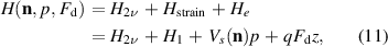

Figure 15. Electric-field-induced and strain-tunable EPS. (a) Artistic picture of the device consisting of a QD-containing diode-like membrane integrated onto a PMN-PT actuator. (b) Color-coded PL spectra from QDs by changing Fd at fixed Fp. (c) Color-coded PL spectra from the same QDs by changing Fp at fixed Fd. (d) Exciton energy as a function of Fp for different Fd. The inset shows the curve of exciton energy shifting with Fd at  . (e) FSS as a function of exciton emission energy for different Fd. (a)–(e) Reprinted with permission from [61]. Copyright (2017) American Chemical Society.
Download figure:
Standard image High-resolution image
 is the electric-field-induced perturbation term additional to the strained system. Diagonalization of the above Hamiltonian spanning the basis of the two bright exciton states gives the FSS:

where  accounts for the difference of the exciton dipole moments. For the specifically selected QDs with polarization along the [110] ([1–10]) direction,
  ∼ 0, and
  ∼ 0, and thus the zero FSS can be achieved when Fd and p take the form p= −(2δ0 + γ0
Fd)/α. This dictates that the zero FSS can be always realized for continuously varying the applied electric field. The experimental verification of this theoretical model is shown in figures 15(d) and (e). The exciton energy has linear dependence of Fp for a given Fd. The inset of figure 15(d) shows the curve of the exciton energy shifting with different values of Fd at
∼ 0, and thus the zero FSS can be achieved when Fd and p take the form p= −(2δ0 + γ0
Fd)/α. This dictates that the zero FSS can be always realized for continuously varying the applied electric field. The experimental verification of this theoretical model is shown in figures 15(d) and (e). The exciton energy has linear dependence of Fp for a given Fd. The inset of figure 15(d) shows the curve of the exciton energy shifting with different values of Fd at  , which can be exactly attributed to the quantum-confined Stark effect. Besides it is clear that the FSS can pass through zero via sweeping Fp for a given Fd (see figure 15(e)). A broad tuning range of 4.6 meV for the exciton emission energy at
  is achieved which can be larger if Fd is further extended.
7. Conclusions and outlooks
Strain is ubiquitous in semiconducting materials and exerting mechanical strain field to low-dimensional semiconducting nanostructures, such as self-assembled QDs and TMDs, is a natural choice for engineering the electronic and optical properties. Remarkably this method has ensured the pace of steady improvements in the performance of QD-based quantum light emitters. Thus far, we have not only summarized the relevant theoretical models to understand the substantial impacts of different configurations of stressors on the optical properties of QDs, but we have also presented the recent progress of employing mechanical strain fields to control the optical properties of QD-based quantum emitters for the realization of advanced functionalities, for instance, defect-based QD SPSs and TMD MLs, wavelength-tunable SPLEDs, EPLEDs, scalable EPSs, hybrid quantum systems based on self-assembled QDs and microcavities as well as the quantum interfaces between solid-state QD-based EPSs and atomic ensemble. In this review we have limited our discussions on the strain engineering of QD-based nonclassical light sources with photon emission energy in the visible and near infrared range. We shoud point out that the strain engineering technique is also valid for narrow band gap semiconducting materials with photon emission in the telecom window. By integrating InAs self-assembled QDs onto piezoelectric substrates, recent works have demonstrated that the mechanical strain fields can be applied to engineer both the energy of single photons and biexciton-exciton photon pairs at telecom wavelengths [153, 154]. Although the material system is different, the underlying strain tuning mechanism that explained extensively in the above text is still applicable.
This review somehow provides a guidance for the future development of high performance QD-based nonclassical light sources involving strain tuning techniques. Despite the considerable progress in strain engineered low-dimensional semiconducting quantum light emitters, the realization of future scalable quantum networks and quantum photonic circuits is still challenging. To achieve such scalable on-chip applications with QD-based SPSs and EPSs, great efforts are still needed to fabricate micro-structured piezoelectric devices so that the integrated QDs on a single chip can be engineered by different strain fields. To this end, mature microfabrication techniques could be possibly utilized to design and fabricate elaborated MEMS structures by using thin film of PZT or single crystal PMN-PT. Meanwhile, the direct growth of piezoelectric thin film by using pulsed laser deposition or radio frequency sputtering deposition can also be deployed for the on-chip integration of strain 'tuning knobs' [155]. In order to achieve efficient optical interconnection via fibers or within silicon photonic chips, the strain-induced nonclassical light sources based on QDs at telecom wavelengths deserve further investigation. Beyond the semiconducting materials, strain engineering is also a plausible tuning technique for other materials which are possibly demonstrated for nonclassical light sources. These materials include color centers in diamond [156, 157] and silicon carbide [158, 159], molecules [33–35] and so on. In summary, the attractive strain engineering technique provides a robust tuning method for tailoring the electronic and optical properties of a variety of low-dimensional semiconducting quantum emitters, which would open a way towards very competitive semiconductor based SPSs and EPSs for the realization of future envisaged large-scale quantum network applications.
Acknowledgments
This work was supported by National Key Research and Development Program of China (2017YFA0206403), National Natural Science Foundation of China (61475180), Science and Technology Commission of Shanghai Municipality (16ZR1442600), Strategic Priority Research Program of Chinese Academy of Sciences (XDB24020400), Shanghai Municipal Science and Technology Major Project (2017SHZDZX03), Shanghai Sailing Program (18YF1428100), Shanghai Rising-Star Program (19QA1410600), Program of Shanghai Academic/Technology Research Leader (19XD1404600), National Natural Science Foundation of China (No. U1732268, 61874128, 11622545, 61851406, and 11705262), Frontier Science Key Program of Chinese Academy of Sciences (No. QYZDY-SSW-JSC032).