
Abstract
In this review paper, we present a comparative analysis of the electrochemical dissolution of III–V (InP, GaAs, GaN), II–VI (ZnSe, CdSe) and SiC semiconductor compounds. The resulting morphologies are discussed, including those of porous layers and networks of low-dimensional structures such as nanowires, nanobelts, and nanomembranes. Self-organized phenomena in anodic etching are disclosed, leading to the formation of controlled porous patterns and quasi-ordered distribution of pores. Results of templated electrochemical deposition of metal nanowires, nanotubes and nanodots are summarized. Porosification of some compounds is shown to improve luminescence characteristics as well as to enhance photoconductivity, second harmonic generation and Terahertz emission. Possible applications of porous semiconductor compounds in various areas are discussed.
Export citation and abstract BibTeX RIS

Original content from this work may be used under the terms of the Creative Commons Attribution 4.0 license. Any further distribution of this work must maintain attribution to the author(s) and the title of the work, journal citation and DOI.
1. Introduction
The wide class of porous materials includes both organic and inorganic materials such as porous metals, porous semiconductor and dielectrics, porous ceramics, polymer foams, and metal-organic frameworks [1–3]. Porous solids often serve as structural bodies in nature, including in wood, bones and other biological objects. Depending on their nature, porous materials are prepared by specific technologies involving a lot of fundamental concepts, and specific fields of applications are determined by their properties.
Among semiconductor materials, considerable interest has been triggered by the discovery of luminescent porous Si three decades ago [4]. The efficiency of porous silicon LED's has risen by 5 orders of magnitude over the years and is currently approaching commercial viability for some integrated display applications [5]. During this time, it was shown at the laboratory research level that porous Si is suitable for many applications, including optic and optoelectronic applications (light emitting devices, optical waveguides, photonic crystals, optical resonators, distributed Bragg reflectors and diffraction gratings), electronic applications (gas sensing, gettering, lithium-ion batteries, and solar cells antireflection coatings), microfluidics, medical applications, etc [6–10].
Recently, it was proposed to produce size-controlled nanocrystalline (nc-Si) dot colloids by exposing porous silicon (PSi) in solvents to pulse laser, which results in fragmentation of the PSi layer with a considerably higher yield than the conventional techniques [11]. This was shown to pave the way for emerging functions of nanostructured PSi related to strong visible photoluminescence of about 40% in quantum efficiency in the red band, efficient quasi-ballistic hot electron emission from an nc-Si diode due to multiple-tunneling transport mode through nc-Si dot chain, and enhanced to a practical level thermo-acoustic conversion due to an extremely low thermal conductivity and volumetric heat capacity of the nc-Si layer. Applications of the quasi-ballistic electron source in flat panel display, multibeam parallel lithography, high-sensitivity image sensor and reductive deposition of thin films have been demonstrated.
Meanwhile, the transition of the porous silicon from academic studies to industry is in progress. Prototype devices on large area wafers taking advantages of the isolating properties of PSi, including power AC switches, radio-frequency (RF) devices and energy micro-sources, have been demonstrated through collaboration between GREMAN and ST Microlectronics [12]. Nevertheless, wide implementation of PSi in the field of electronic component manufacturing still needs significant investment, development, optimization and validation of reliable equipment and processes in terms of throughput. BOSCH GmbH uses PSi in high-volume industrial production of micro-electro-mechanical (MEMS) devices, particularly in the manufacturing of monolithically integrated pressure sensors [13]. SOLEXEL, in collaboration with SCREEN, is particularly active in the field of photovoltaic cells manufacturing with the design and the development of high throughput production equipment [12].
On the other hand, the development of technological methods for the preparation of porous alumina templates, including the ones with periodically ordered pore arrangement, triggered extensive activities in research for template synthesis of various nanoscale materials, with it being an elegant, inexpensive, and technologically simple approach [14].
Porous anodic aluminum oxide (AAO) attracted a huge interest due to the pioneering works of Martin [15] and Masuda and Fukuda [16]. Self-organized nanoporous structures with hexagonal ordered distribution of pores were obtained on a highly pure Al surface via electrochemical anodization in acidic medium [17, 18]. AAO templates have many advantages over the polycarbonate membranes, such as high pore density, thermal stability, cost effectiveness and versatility. Pore diameter, length, inter-pore spacing, and pore ordering can be easily tailored by tuning the anodizing parameters such as voltage, time, electrolytes, pH value, and temperature [18].
Both of these materials are prepared by electrochemical etching of Si wafers in the case of porous Si, and Al wafers in the case of porous alumina templates. Electrochemistry offers an accessible and cost-effective approach for the preparation of porous templates with tailored architecture on the submicrometer scale. However, Si is a material with indirect energy band gap corresponding to the infrared spectral range, which strongly restricts the area of applications for porous Si. On the other hand, porous alumina templates exhibit high resistivity and therefore they often play a passive role in nanofabrication processes, since they are used mostly for the templated synthesis of nanowire arrays which are prospective for several applications [19]. The templated growth of nanowires via electroplating is provided usually by the metal contact deposited on the back side of the high-resistivity membranes. To produce electroplating of metal nanodots and nanotubes into alumina templates, additional technological steps are required, e.g. chemical modification of the inner surface of the pores prior to electrodeposition, which leads to the incorporation of spurious phases in the nanotube walls [20].
Semiconductor nanotemplates, the properties of which can be easily controlled by external illumination, applied electric fields, etc, provide wider possibilities for nanofabrication. The production of nanodots, nanotubes and 2D metallo-semiconductor interpenetrating networks are promising for various nanoelectronic, optoelectronic, plasmonic, and nanophotonic applications. Metal nanodots are obtained routinely in solutions, but positioning them on a chip remains a significant challenge. Conventional controlled patterning approaches like electron beam lithography [21], stencil lithography [22, 23], and extreme ultraviolet interference are very expensive. In spite of the fact that low-cost alternatives such as nanoimprint [24] and nanosphere techniques [25] exist, they are limited because they imply complicated resists, lift-off processes, and cannot be accurately controlled as to their positioning, size, and shape.
The optoelectronic applications of metallic nanotubes are based on the extended dielectric/metal interface that can sustain the propagation of electromagnetic waves coupled to collective oscillations of the conduction electrons in the metal, the so called surface plasmon polaritons, allowing the manipulation and transmission of light on the nanoscale [26, 27]. 2D metallo-semiconductor networks may find potential applications in photonic integrated devices and circuits [26].
Since semiconductor compounds provide more space for tailored nanofabrication in terms of compositions, bandgaps, mechanisms of the pore growth and new properties with large potential for applications, their porosification was widely explored over the last two decades. This review will focus on the different aspects of pore growing, including self-organized pore formation which results in the production of ordered arrangements of pores; on properties of the produced semiconductor compound porous materials and nanocomposites on their basis; and on various actual applications and future prospects.
The paper is organized as follows. Section 2 introduces the electrochemical dissolution mechanisms for the porosification of various semiconductor materials with a main focus on III–V and II–VI compounds, followed by the description of approaches for obtaining morphologies related to networks of nanowires, nanobelts and nanomembranes as well as technologies for electrochemical deposition of metal nanostructures into porous semiconductor templates. Section 3 describes self-organized phenomena occurring under special conditions of electrochemical etching, which open possibilities for the formation of single crystals of pores, multilayer porous structures and nanocomposite materials. Section 4 is dedicated to the review of basic properties of porous materials as compared to their bulk counterparts with a main focus on luminescence, photoconductivity, optical phonon engineering and nonlinear optical properties. Section 5 analyses the state of the art and prospects for use of the advantageous properties generated by the electrochemical porosification in various applications. Finally, conclusions and outlooks are formulated.
2. Electrochemical dissolution mechanisms: comparative analysis of III–V compounds (InP, GaAs, GaN), II–VI compounds (CdSe, ZnSe, ZnxCd1-xS), and SiC
2.1. Dissolution mechanisms and types of pores: crystallographically oriented, current line oriented, and fractal pores
Over the last few decades, it was demonstrated that electrochemistry is one of the most accessible and cost-effective approaches for tailoring the architecture of semiconductor materials at the nanoscale level by introducing porosity. One of the key problems with electrochemical (EC) methods introducing porosity in semiconductor materials is the appropriate choice of the electrolyte composition. This problem is solved individually for each material. Due to the narrow band gap of InAs, it is relatively difficult to reach nanostructuring in this compound via electrochemical etching techniques. Nevertheless, the formation of InAs micro- and nano-pencils was reported [28]. However, the obtained structures are inhomogeneous. More recently, it was shown that the morphology of the porous InAs layers can be controlled by the composition of the electrolyte and the applied electrochemical parameters [29]. It is difficult to control the mechanism of pore growth in InAs, since in narrow bandgap semiconductors uniform electrochemical etching proves to occur simultaneously with the pore growth, thus resulting in the limitation of the achieved depth of the produced porous layer.
Usually, three types of pores can be generated in semiconductor compounds: current line oriented (CLO or curro pores), crystallographically oriented (CO or crysto pores), and fractal pores. The characteristics of the pores (shape, velocity of growth, etc) depend on the specific anodization conditions [30]. It was established that CO pores grow at current densities lower than a certain threshold value, whereas CLO pores grow at current densities higher than the threshold value. The threshold values depend strongly on the free carrier density in semiconductor crystal, electrolyte concentration, and temperature. The main feature of the CO pores is that they grow along definite crystallographic directions. In case of sphalerite crystal structures, they grow along <111> B crystallographic directions, independent of the initial surface orientation, the angle between pores being approximately 109° as shown in figures 1(a) and (b). They tend to have a triangular cross-section, with the pore walls and tips showing a pronounced crystallographic anisotropy as well [31]. A very important property of the crysto pores is their ability to intersect each other, thus opening a new way for semiconductor 3D structuring, seen in figure 1(c). Crysto pores are inherent to Si, GaP, InP and GaAs, however no crysto pores have been observed up to now in II–VI semiconductor compounds such as ZnSe and CdSe. On the other hand, curro pores are inherent to Si, GaP, InP and ZnSe, as shown in figures 1(d) and (e), however no curro pores have been observed so far in GaAs. No intersection of curro pores was demonstrated experimentally up to now.
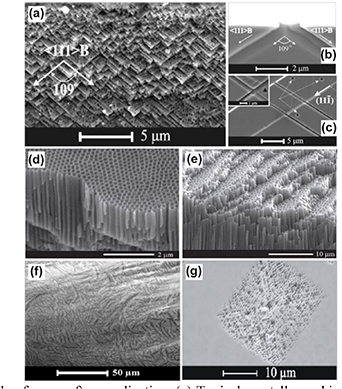
Figure 1. Example of pores after anodization. (a) Typical crystallographically oriented pores in (100)-oriented n-InP; Crysto pores in GaAs: (b) pore growth along <111> B directions in GaAs and triangular cross-section shape as well as intersection of pores in (c). Current line oriented pores in InP (d) and ZnSe (e). (f) Fractal pores in ZnSe, cross-section. (g) Fractal like pores in GaAs, top view. [31] © John Wiley & Sons. Copyright © 2003 WILEY-VCH Verlag GmbH & Co. KGaA, Weinheim.
Download figure:
Standard image High-resolution imageFractal pores are the third type of pores observed in Si, III–V and II–VI semiconductor compounds. A fractal is normally defined as an object that can be divided into parts, and each of these parts will be similar to the original object. The structures presented in figures 1(f) and (g) are not perfect fractals, but the pores are called fractal due to their fractal-like way of growth, i.e. each point of a pore in such a structure can be a source for one or more similar pores growing in totally different directions. The existence of fractal pores not only opens new insides regarding the mechanism of pore formation in semiconductors, but it is also interesting for optical applications, for example nonlinear optical effects.
In the case of InP, at the beginning of the anodization process, multiple branching of a primary pore in the nucleation layer results in a whole set of secondary pores oriented along crystallographic directions <111> B. The end points of the set of pores originating from the same root nucleus form a linear domain and serve as the nuclei for a corresponding domain of CLO pores, as shown in figure 2(a). Thus, in case the nucleation layer is well developed, there is a general tendency of current line oriented pores to form rows oriented along the <110> direction. This tendency, accompanied by the repulsive pore–pore interaction due to overlapping space charge regions surrounding neighboring pores, leads to the observed ordered close packed 2D distribution of CLO pores, which will be described in section 3.
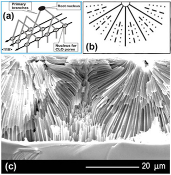
Figure 2. Schematic outline of the development of the porous structure in (a) III–V and II–VI (b) during anodic etching (see text for details). (c) Development of the porous structure in CdSe after neighboring domains meet. Reproduced from [32]. © IOP Publishing Ltd. All rights reserved.
Download figure:
Standard image High-resolution imageThings are different in the case of CdSe. At the beginning of anodization, the etching starts at surface imperfections. After the initial pitting of the surface, further etching proceeds in all directions, i.e. in the first approximation radially away from the surface imperfections, leaving the top surface of the sample practically intact. As a result, a porous domain forms around each etching pit. After neighboring porous domains meet, a continuous porous network emerges with parallel pores that continue to grow, under the applied voltage, in the direction perpendicular to the initial surface of the sample. The extension of a porous domain in CdSe until it joins the continuous porous network is illustrated in figure 2(c). The pores obviously grow perpendicular to the equipotential lines of the electric field in the anodized sample. The total number of pores is actually defined at the very beginning of anodization when an interesting process of pore multiplication occurs that is based on the doubling principle [32]. Namely, in the first instants of the pore etching, the number of pores progressively doubles until an equilibrium value of the ratio between pore diameter and wall thickness is reached. Figure 2(b) shows schematically the essence of the doubling principle in pore growth.
Figure 3 presents SEM images of electrochemically etched InP, ZnSe and Zn0.4Cd0.6S crystals [28, 30] with the anodization potential intentionally changed during the pore growth. It is evident from figure 3(a) that the change of the applied potential during anodization of InP crystals from high to low values leads to a switch in the pore growth mechanism from current-line oriented pores to crystallographically oriented pores, which will be discussed in more details in section 3. In contrast to this, the change in the applied potential for ZnSe and Zn0.4Cd0.6S single crystals, as seen in figures 3(b) and (c), does not change the pore growth mechanism, current-line oriented pores being produced under both high and low values of the applied potential. Switching from 18 V to 16 V during the etching of Zn0.4Cd0.6S just leads to the decrease in the pore diameter from 30 nm to around 15 nm, rather than to the commutation from current-line oriented pores to crystallographically oriented pores.

Figure 3. SEM image of porous InP (a), ZnSe (b), and Zn0.4Cd0.6S (c) layers anodized with changing the applied potential [from 7 V to 1 V in (a); from 15 V to 13 V in (b); and from 18 V to 16 V in (c). [31] John Wiley & Sons. Copyright © 2003 WILEY-VCH Verlag GmbH & Co. KGaA, Weinheim.
Download figure:
Standard image High-resolution imageThe lack of crystallographically oriented pores in II–VI semiconductors looks curious since, e.g., ZnSe has the same zinc-blend crystal structure as GaAs, GaP and InP. This can be explained taking into account the nature of chemical bonds between constituent atoms. Covalent tetrahedral bonds due to sp3 hybrid orbitals are inherent to elemental semiconductors such as Si and Ge. Tetrahedral bonds are also inherent to compound semiconductors. However, in this case the chemical bonds can be both covalent and ionic, since the semiconductor compounds consist of atoms with different electronegativities. Table 1 presents the atom electronegativity difference for some semiconductor compounds calculated using Pauling's law [33]. The electronegativity is an indicative of the strength with which atoms attract electrons. The difference in electronegativities of the constituent elements is therefore indicative of the ionicity, as shown in table 1 [34]. The higher the ionicity, the stronger the attraction between the atoms. It can be seen from table 1 that the degree of ionicity in III–V semiconductor compounds is lower compared to the II–VI compounds. As a result, crystallographically oriented pores can be obtained in III–V compounds, in contrast to II–VI compounds.
Table 1. Values of electronegativity difference and degree of ionicity in II–VI and III–V semiconductor compounds.
| II–VI | III–V | |||||||
|---|---|---|---|---|---|---|---|---|
| Compound | ZnO | ZnS | ZnSe | CdSe | InP | InAs | GaAs | GaP |
| Electro-negativity difference | 2 | 1 | 0.9 | 0.9 | 0.6 | 0.5 | 0.5 | 0.32 |
| Ionicity (%) | 63 | 22 | 19 | 19 | 11 | 9 | 9 | 2 |
Let's move on to GaN, which represents a class of wide-bandgap III–V semiconductor compounds. Earlier investigations demonstrated that photoelectrochemical etching results mainly in the fabrication of nanowires or pyramidal structures consisting of nanowires, which represent threading dislocations [35]. It was recently shown that porous GaN can be produced in metal organic chemical vapor deposition (MOCVD) grown GaN layers by electrochemical etching, and the degree of porosity can be controlled by both the anodic voltage and sample doping [36, 37]. Aligned and exposed mesopores in single crystalline GaN formed in nitric acid were reported [38]. It was shown that, like in the case of InP, a nucleation layer is formed on the top surface which can be removed via UV-assisted anodic etching at low voltages. Moreover, combining electrochemistry with thermal treatment of porous substrates offers the possibility to release the free-standing porous membrane [39].
On the other hand, to assure further progress in the development of III-nitride-based power electronics and high brightness light emitting devices, high quality single crystalline GaN substrates are needed, since the thickness of MOCVD-grown layers is usually limited to 2–3 µm, and these layers suffer from internal strains and defects due to significant mismatches of crystal lattices and thermal expansion coefficients with the sapphire, Si or SiC usually used substrate material.
Hydride vapor phase epitaxy (HVPE) has been identified during the last decade as one of the most relevant techniques for the growth of bulk GaN for substrates. HVPE ensures the highest growth rates (up to 500 μm per hour) and favors the growth of thick GaN layers which are subsequently detached from the sapphire or other foreign substrates [40]. In recent years, many teams have focused their research on porosification of HVPE grown free-standing GaN substrates and fabrication of high aspect ratio GaN nanostructures [41, 42]. According to Ref. [43], the surface morphology of the photo-etched GaN consists of islands dispersed amongst concentric rings of alternating small and large pores. Further research using photoelectrochemical and electrochemical etching techniques brought to light self-organized three dimensional nanostructured architectures which were attributed to the spatial modulation of the electrical conductivity generated during HVPE growth of GaN [44]. The specific features of self-organized 3D nanostructured architectures including quasi-ordered concentric hexagonal structures have been disclosed due to the fact that electrochemical and photoelectrochemical etching techniques are highly sensitive to local doping. Recently, different porous morphologies produced by anodization in the depth of a HVPE-grown GaN substrates with respect to the N- or Ga-face were reported [45]. Complex porous pyramidal-type structures are formed at a depth of several tens of micrometers from the N-face, while homogenous porous matrices with pores oriented perpendicular to the wafer surface are generated at a depth of up to 50 μm at the Ga-face.
The features of SiC porosification will now be discussed. The pioneer work on the electrochemical porosification of 3C-SiC was reported by Takazawa et al [46]. According to recent publications [47, 48], electrochemical etching of low resistivity n-type SiC wafers results in the formation of two nanostructured products: porous SiC with a well-ordered crystalline structure and oligomeric compound named carbon fluorooxide (CFO). It has been established that the increase in HF concentration, presence of ethanol in the etchant, increase in SiC electrical conductivity and decrease in etching current density leads to an increase in CFO/SiC ratio in the etching product and an increase in the degree of porosity. As a result, the SiC morphology changes from macroporous tubular through mesoporous hierarchical to a mesoporous filamentary one. Note that porous SiC has found applications in electronic devices and has promising applications in sensing [49].
The results of a comparative analysis of the pore growth in II–VI and III–V compounds during electrochemical etching are summarized in table 2. Difficulties with controlled pore formation are evidenced in narrow badgap semiconductors. The absence of crysto pores in II–VI compounds and their growth in III–V compounds are explained in terms of bonds iconicity. Curro pores grow practically in all compounds with the exception of GaAs. However, in II–VI compounds, curro pores grow in a large diapason of potentials applied during electrochemical etching, while in III–V compounds they grow only at high values of the applied voltage. The issue with the absence of curro pores in GaAs needs additional investigation.
Table 2. Types of pores in semiconductor compounds.
| Type of pores, Determining factor | II–VI | III–V | ||||||
|---|---|---|---|---|---|---|---|---|
| ZnSe [29] | CdSe [32] | ZnCdS [29] | InP [31] | GaAs [30, 31] | GaP [31] | GaN [37, 38, 45] | InAs [28, 29] | |
| Crysto pores | No | No | No | Yes, low volt. | Yes | Yes, low volt. | Yes, low volt. | No |
| Determining factor | High ionicity | Low ionicity | Narrow bandgap | |||||
| Curro pores | Yes | Yes | Yes | Yes, high volt. | No | Yes, high volt. | Yes, high volt. | No |
| Determining factor | Not influenced by ionicity | Not influenced by ionicity | Narrow bandgap | |||||
| Fractal pores | Yes | No | No | No | Yes | No | No | No |
| Determining factor | Not identified | Not identified | ||||||
2.2. The choice of electrolytes. Porosification in neutral electrolytes
Usually, the pores in semiconductors are introduced via electrochemical dissolution of materials in electrolytes containing acids such as HF, HCl, H2SO4, HNO3, etc, or in alkaline electrolytes. The nature of the electrolyte and its concentration strongly influences the morphology of porous layers produced via the anodization process.
In the last decade, to make the process of nanofabrication based on anodic etching broadly accessible and environmentally friendly, a part of research was focused on nanostructuring in neutral electrolytes. Tiginyanu et al [50] proposed to use a neutral electrolyte based on an aqueous solution of NaCl instead of commonly used aggressive acids or alkaline electrolytes for the purpose of electrochemical nanostructuring of semiconductor substrates. The possibilities for controllable porosification of GaAs and CdSe substrates by anodic etching in an environmentally-friendly neutral electrolyte based on aqueous solution of NaCl have been demonstrated. Moreover, the photoluminescence investigation of the prepared porous structures showed no decrease in the near-bandgap emission intensity, in spite of the huge surface inherent to the porous skeleton. This implies that the surface recombination rate does not increase in porous samples, which is indicative of an effective passivation of the huge internal surface of the porous samples during anodization in the NaCl-based electrolyte. Later on, formation of uniform porous layers and porous InP membranes was realized for various applications, e.g. nonlithographic manufacturing of semiconductor nanotemplates for the deposition of metal nanotubes [51], and the development of gas sensors was demonstrated [52].
Anodization in salty water proves to be a powerful tool for manufacturing 3D ordered porous structures in InP [53]. Depending on anodization conditions, a spatial nanostructuring can be easily realized. For the fabrication of 2D porous structures, the anodic etching is carried out under constant applied voltage (5 V), while for 3D structures the value of the applied voltage between the reference electrode and working electrode is periodically modulated in three steps (2 V, 4 V and 6 V) for a duration as long as 10 s each. Spectacular wavy entities can be fabricated using switches from crysto pores to curro pores and vice versa, as shown in section 3.
Electrochemical nanostructuring in neutral electrolyte proves to be feasible for nanostructuring narrow band gap III–V semiconductor compounds. InAs is a direct band gap semiconductor compound with zinc blende structure and a narrowest energy gap among the III–V binary compounds, except for InSb. As mentioned above, due to the narrow band gap of InAs, it is relatively difficult to reach nanostructuring in this compound using electrochemical etching techniques. Nevertheless, a comparative anodization in acids and NaCl was investigated and the formation of InAs micro- and nano-pencils was reported by Sirbu et al [54].
The electronic band gaps of InAs, InP, GaAs and CdSe are respectively 0.35; 1.3; 1.4 and 1.7 eV at 300 K, which means that the nanotemplates based on these materials are opaque in the visible region of the spectrum. At the same time, GaN with the bandgap as high as 3.4 eV at 300 K is a perspective candidate for the fabrication of conductive nanotemplates transparent in the whole visible region of the spectrum.
Schwab et al reported results of MOCVD grown n-GaN nanostructuring in 0.3 M NaNO3 and 3 M NaCl neutral electrolytes [55]. It was demonstrated that the etching behaviors in NaNO3 and HNO3 electrolytes are very similar and etching has a minimal impact upon the produced morphologies characterized by propagation of pores parallel to the current flow, with the exception of a thin nucleation layer at the surface. At the same time, the use of NaCl implies the formation of crystallographically oriented pores exhibiting characteristic triangular cross-section at applied voltage of 6 V for 30 min. Even at increased applied anodization voltages of up to 30 V, the pores exhibit preferential growth along crystallographic directions. Note that the entire 2 μm thick MOCVD grown GaN layer can be fully etched in 1 s and 2 s at 30 V and 20 V, respectively, due to the high etch rate in NaCl electrolyte.
Growth of crystallographically oriented pores in highly doped GaN layers looks curious because the formation of such kind of pores is characteristic for low doped samples or low applied voltages [31]. A comparative study of HVPE-grown GaN etching in HNO3, HCl, and NaCl solutions performed recently on Ga- and N-faces of crystalline substrates demonstrated that GaN can be efficiently porosified in 3.5 M NaCl electrolyte [45].
The increase of the anodization potential in the electrochemical etching process leads to the increase of the pores diameters [36] with the simultaneous reduction of the pore wall thickness which comprises two space charge regions. At some critical values of the potential an electro-polishing process can be initiated [55]. Based on these considerations, Gao et al [56] reported on the fabrication of self-standing GaN-based film with multiple quantum well (MQW) structure via an electrochemical etching technique in neutral electrolyte by switching the etching potential from 20 to 40 V at the end of anodization. The schematic representation of the electrochemical etching approach to produce free-standing GaN-based porous membranes is presented in figure 4(a).

Figure 4. (a) Schematic illustration of the electrochemical etching approach to produce free-standing GaN-based membranes and (b) transferred large-area nanoporous GaN-based membrane on a target substrate (a tape was used as an example). Reprinted from [56], Copyright (2017), with permission from Elsevier.
Download figure:
Standard image High-resolution imageThe analysis shows that, in spite of the fact that the etching behavior is mainly pertinent to anions, the cations also determine the peculiarities of GaN anodic etching [58]. The gallium-related intermediate product of photo-assisted anodic etching is generally believed to be gallium oxide Ga2O3. Since this oxide is not soluble at a neutral pH, there is an indication that another etching mechanism exists for neutral electrolytes. The analysis of data in table 3 also shows that, while electrochemical porosification of III–V semiconductor compounds in environment-friendly electrolytes was well explored, less attention has been paid to II–VI compounds. This issue needs further investigation and technological development.
Table 3. Semiconductor compounds suitable for nanostructuring in neutral electrolytes.
| Semiconductor compound | Typical electrolyte for anodization | Possibilities of anodization in environment-friendly electrolytes | ||
|---|---|---|---|---|
| III–V | InP | HCl [29, 31] | NaCl [51–53, 57] | |
| GaAs | HCl; H2SO4 [30, 31] | NaCl [50] | ||
| GaN | KOH [37]; HCl [37, 45]; H3PO4 [37] HNO3[37, 45, 58] | NaCl [45, 54]; NaNO3 [55, 56] KNO3 [58] (BMIM)ClO4 ionic liquid [59] (EMIM)(OTF) ionic liquid [42] (EDTA-2Na) [60] | ||
| InAs | H3PO4:HNO3 [28] KOH [29] | NaCl [54] | ||
| GaP | HCl; HNO3; H3PO4; HBr [31, 61, 62] | Not reported yet | ||
| II–VI | CdSe | HCl [32] | NaCl [50] | |
| ZnSe | K2Cr2O7:H2SO4 [29, 57] | Not reported yet | ||
| ZnCdS | HCl [29]; HNO3 [63] | Not reported yet | ||
According to the data presented in table 3, among III–V compounds the main interest was focused on gallium nitride, taking into account its prospects for various microelectronics, optoelectronic and photonic applications. Some peculiarities of GaN porosification in a neutral aqueous NaCl electrolyte are summarized in table 4.
Table 4. Some features of electrochemical porosification of GaN with doping density of around 1019 cm−3 in acid HNO3 and neutral NaCl electrolytes.
| Electrolyte used | Acid HNO3 | Neutral NaCl |
| Anodic potential for crysto pore growth | Up to 5 V | Up to 20–30 V |
| Pore growth mechanism | Neighboring pore interaction | Avalanche breakdown |
| Rate of pore penetration | 0.05 µm s−1 | 1 µm s−1 |
| Ref. | [45] | [55] |
As seen in table 4, crysto-pores grow in GaN up to much higher anodic potentials when anodization is performed in a neutral NaCl electrolyte as compared to anodization in an acid electrolyte, where no crysto-pores were observed at respective potentials, exclusively curro-pores being formed. The pore growth mechanisms are also different for anodic etching in neutral and acidic electrolytes. At the same time, the rate of pore growth in GaN is by more than an order of magnitude higher upon anodization in the neutral electrolyte.
2.3. From porous structures to networks of nanowires, nanobelts and nanomembranes. Metal-assisted photochemical etching
In the last few years, considerable research efforts have been focused on one-dimensional (1D) nanostructures, such as nanorods, nanowires, nanobelts, and nanotubes with well-controlled sizes, morphologies, and geometries, due to the quantum size effects which resulted in fascinating properties and novel applications in nanooptoelectronic and nanosensor devices. In particular, semiconductor nanowires are predicted to drive new generations of compact, ultrafast, and high efficiency electronic and optoelectronic devices.
At the same time, two-dimensional (2D) nanomaterials which are characterized by a thickness of the order of nanometers and a lateral scale much bigger than that of nanobelts, including nanosheets and nanoplates, receive much less research attention than 0-D (nanoparticles and quantum dots) and 1D materials. A small number of reports on 2D semiconductor nanosheets and related devices have been published. The main reason is related to the difficulty to obtain high-quality 2D semiconductor nanosheets with appropriate electron or hole concentrations required for device applications.
Semiconductor nanowires of different compositions have been prepared by a variety of methods, including laser ablation [64–66], template-assisted electrochemistry [67–69], chemical transportation [70], chemical vapor deposition [71] and solvothermal methods [72, 73]. However, the nanowires obtained by using these techniques have crystallographic defects due to impurities from electrolytes, precursors and different transport gases in the growth process. It was shown that the mobility in InP nanowires is significantly degraded by the presence of planar crystallographic defects [74]. These defects are also responsible for the spatial separation of electrons and holes which rapidly quench nanowire PL. Future nanowire-based devices require very high crystal quality of constituent InP nanowires. According to the literature data, the growth of defect-free nanowires with high crystalline quality is still a technological challenge.
All of the mentioned above technologies represent bottom-up approaches. An alternative and cost-effective technology for the fabrication of low-dimensional nanostructures proves to be anodic etching of bulk semiconductor crystals. By choosing the optimal electrochemical conditions, it is possible to obtain a huge amount of semiconductor nanowires connected to the bulk substrate. Usually, the wire formation procedure passes through the pore formation in the anodization process, but it is relatively difficult to identify the time when the electropolishing process starts.
Li et al studied the I–V curves of the anodic etching of GaAs crystals and showed that the anodization can be divided into three regions, depending on the formation potential: pore/wire formation (3–4.5 V), texturing (4.5–6.6 V), and electropolishing (above 6.6 V) [75]. The electrochemical dissolution behaviors of the investigated n-type (100) GaAs crystals doped with Si (2.67–8.63 × 1017 cm−3) in a 5% KOH electrolyte was found to be characterized by the I–V curve shown in figure 5(a). It can be seen that a very low current level was registered when the applied potential was lower than the breakdown potential or pore formation potential (PFP) equaling 3 V. Further increase in the potential leads to the current rise due to the avalanche breakdown mechanism. Under such conditions pores and wires are obtained. Above the peak value Vps at 4.5 V a decrease in the current density was recorded. SEM investigation of samples in this region disclosed a surface texture without generated pores, while at higher applied potential electropolishing occurs.
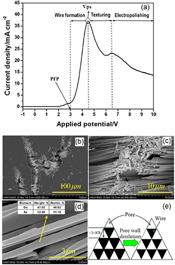
Figure 5. (a) I–V plot of the n-GaAs (001) smooth surface swept in 5% KOH at a scan rate of 5 mV s−1. (b–d) Different magnification plan-view SEM images of GaAs wires etched at 3 V. The inset in (d) shows EDX data extracted from the nanowires. (e) Illustration showing the wire formation procedure. Reprinted from [75], Copyright (2011), with permission from Elsevier.
Download figure:
Standard image High-resolution imageAs mentioned above, due to the fact that As is more easily oxidized than Ga, pores were always found to grow along the <111> B directions [31]. Figures 5(b)–(d) illustrates GaAs wires, tilted to the surface along <111> B directions, with diameters ranging from 400 to 700 nm.
Normally, it is considered that the thickness of the pore walls is determined by the space charge region (SCR) effect. Langa et al reported that the distance between the centers of two pores must be at least one pore diameter plus twice the width of the SCR around a pore [76]. Namely, a wall with the thickness of two space charge regions remains between the two neighboring pores due to the two semiconductor/electrolyte junctions. So, Li et al calculated the width of the SCR to be approximately 150 nm when the voltage drop across the SCR was 3 V. Taking into account that the nanowire formation requires higher applied potential, this value is roughly in accordance with the obtained diameter of the GaAs nanowires.
The authors proposed and explained the formation of the GaAs nanowires, as seen in figure 5(e). In the case when the pore walls become thin enough to approach twice the space charge region width, holes cannot diffuse further into the interface region since hole diffusion is required to pass through the carrier depleted SCR. This behavior finally terminates the pore wall dissolution reactions, which stabilizes the wall morphology. Note that due to the fact that pores in GaAs possess a triangular cross-sectional shape, the resulted nanowires also have a triangular shape.
For some applications, it is necessary to prepare nanowires aligned vertically to the substrate surface. In 2014, Asoh et al succeeded to fabricate high-aspect-ratio GaAs nanowire arrays self-aligned perpendicular to the surface via anodization of n-type (111)B GaAs substrates [77]. In previous works, the authors optimized the electrochemical parameters of the GaAs etching process [78, 79]. It was found that during the anodization process, the nanopores grow in the vertical direction along the <111> crystallographic direction due to the use of (111)B substrates and, at the same time, new etch pits are nucleated. It is important to note that when a (100) oriented GaAs substrate was used, no formation of vertically aligned GaAs nanowires was found because the pores grew obliquely and intersected each other [75, 76]. The approach proposed by Asoh et al has some noteworthy features: (i) during the anodization, the pore diameter is homogenized by a self-regulating process; (ii) when three adjacent pores became interconnected following the dissolution of GaAs pore walls, the GaAs surrounded by the three adjacent pores formed a nanowire with a high aspect ratio; (iii) eventually, self-aligned GaAs nanowires with a uniformly sized triangular cross section formed spontaneously [77]. Free-standing nanowires with uniform diameters of approximately 200 nm and a length of 100 μm were obtained after 30 min of anodization of GaAs substrates with the electron density of (0.9–2.4) × 1018 cm−3. It was shown that the diameter of nanowires can be reduced from 200 nm to 150 nm by combining the anodic etching with post-chemical etching in an etchant consisting of ammonium hydroxide and hydrogen peroxide. Besides, the nanowires were joined tightly together at the surface forming bundle structures. The obtained arrays of bundles were used by authors as an electron field emitter exhibiting a low turn-on voltage and high field-emission current stability.
Litovchenko et al [28] also demonstrated the applicability of electrochemical technologies for nanostructuring of narrow band gap InAs semiconductor surfaces in view of preparing morphologies promising for electron field emission applications. They proposed a new technological approach for the preparation InAs rod-like micro- and nanostructures by applying the anodization voltage in pulses with the amplitude of 6 V and the duration of 1 ms at a pulse repetition frequency of 1 Hz. As a result, a homogeneous cone-like texture with the height of the cones h = 0.5–1 μm and sharp tops of ~100–200 nm was prepared. The obtained InAs nanostructures, as seen in figure 6(a), proved to be efficient electron field emission cathodes with rather high current emission (up to 1 × 10⁻⁵ A cm−2) and good stability in the range of applied voltages of 400–500 V, shown in figure 6(b).

Figure 6. (a) SEM image of InAs nanostructured surface. (b) Current–voltage characteristic of the electron field emission from the nanostructured InAs surface (arrows indicate the change in the slope). Reproduced from [28]. © IOP Publishing Ltd. All rights reserved.
Download figure:
Standard image High-resolution imageTo date, there are a small number of articles regarding electrochemical etching to fabricate p-type semiconductor nanowires. Formation of porous network in a p-type II–VI material, namely, in p-CdZnTe, was demonstrated by Erne et al [80, 81]. At the same time, Zenia et al subjected p-ZnTe crystals to electrochemical etching and illustrated the formation of needle-like structures exhibiting a blueshift of the excitonic transition energies [82]. The authors found that efficient etching occurs in the potential range 0.5 < U < 1.2 V SCE−1, corresponding to current densities of 200 mA cm−2, and established that the etching process is more homogeneous along the surface when the anodization process is performed under galvanostatic conditions at current densities of 200 mA cm−2. Even after prolonged etching, the length of the needle-like structures did not exceed 2 µm. Pulsed electrochemical etching, however, proved to be efficient for anodization of p-type ZnTe, resulting in the formation of 10 μm long nanowires with the diameter of 50 nm [83]. As in the study of Zenia et al, the authors used an electrolyte based on HNO3:HCl:H2O with the ratio 5:20:100, but under the application of 0.3 s voltage pulses with the frequency of 1 Hz and amplitude of 5 V (the pause between pulses was of 1 s). In this approach, the formation of nanowires required about 30 min of anodization. The dynamics from the etch pits formation up to fabrication of nanowires is presented in figures 7(a) and (b), respectively. The high quality of the produced ZnTe nanowires was demonstrated by photoluminescence investigations since the emission intensity and spectral distribution of PL are practically identical to those of the initial bulk material.

Figure 7. SEM view of a ZnTe sample after 15 min (a), and 30 min (b) of electrochemical treatment. Inset is the magnified view of an etch pit. Reproduced with permission from [83].
Download figure:
Standard image High-resolution imageThe preparation of nanowires described above requires at least half an hour of anodization duration. It is possible, however, to fabricate InP nanomembranes and nanowires in a cost-effective way, e.g. using fast anodic etching of n-InP single crystalline substrates under potentiostatic conditions [84]. The authors of [84] used the term 'fast anodic etching' because 2 μm long nanowires are obtained in just 3 s of anodization, which means that the rate of etching in depth direction is about 40 μm min−1 [84]. Applying anodization under 5 V potential to samples with the carrier density of 1 × 1018 cm−3, one can fabricate porous layers with pore diameter and wall thickness about 80 nm and 40 nm, respectively, as shown in figure 8(a). An increase in the applied potential up to 7 V gives rise to pronounced fluctuations in the pore diameter and leads to the formation of highly porous layers, the porous skeleton being characterized by percolation, as presented in figure 8(b). Furthermore, by applying a high-voltage pulse during the anodization, it is possible to detach the obtained porous layer from the substrate, i.e. to fabricate a highly porous membrane. In [84], conventional photolithography was used to open rectangular windows with a breadth of 35 μm in the photoresist covering the top surface of the samples. In this way, porous membranes with predefined width can be easily obtained. Moreover, applying a high-voltage short pulse via photolithographically defined windows before the anodization process leads to the formation of InP nanowalls and nanowires. It was established that the morphology depends drastically upon the value of the applied voltage pulse. As can be seen from figure 8(c), the etching results in the formation of mosaic structures consisting of ultrathin semiconductor walls. At the same time, a relatively large number of nanowires form with diameters of about 50 nm (figure 8(c)). The formation of nanowires starts to predominate with a further increase of the applied voltage. Figure 8(d) illustrates a uniform network of parallel nanowires fabricated by applying pulse voltage of 15 V.
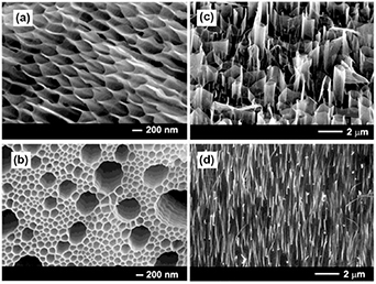
Figure 8. SEM images taken from porous layers fabricated by anodization of bulk n-InP (a) at U = 5 V, (b) U = 7 V, (c) U = 10 V and (d) at U = 15 V. Reprinted from [84], Copyright (2014), with permission from Elsevier.
Download figure:
Standard image High-resolution imageAmong top-down methods, metal-assisted chemical etching (MacEtch), which was proposed by Li and Bohn in 2000, has attracted increasing attention in recent years as a novel micro-nanomachining approach [85]. In contrast to the electrochemical and photo-electrochemical (PEC) etching, MacEtch does not require an electrical contact to be made to the sample. The presence of noble metals accelerates the etching rate underneath them with a 'sinking' effect of the catalytic metal in the semiconductor substrate, acting as a negative resist etch mask. When the semiconductor substrate with deposited metal is immersed in the electrolyte, the surface of the catalytic metal serves as a local cathode and the reduction reaction of H2O2 with electron consumption, i.e. hole (h+) production, is initiated. At the same time, the interface of catalytic metal and semiconductor works as anode leading to the oxidation with the release of electrons. As a result, a local current flow occurs due to the difference of potential. Finally, the formed oxide is soluble in etching solution, causing partial removal of semiconductor without net consumption of the metal.
Based on these considerations, MacEtch proved to be a simple and low-cost method for fabricating various nanostructures, with the ability to control cross-sectional shape, diameter and length, depending on the type and pattern of the catalytic metal thin films or nanoparticles [86, 87]. Patterning of the catalytic metal can be carried out using lithographic and non-lithographic methods. For the preparation by design of a desirable catalytic metal pattern, lithographic methods are used [88, 89]. In the case of non-lithographic methods, various approaches for catalytic metal deposition in the form of a discontinuous layer, islands [90–94] or particles from a colloidal suspension are used [95–98]. Varying the density of particles, islands and cracks of the deposited metal layer determines whether the obtained structures represent porous-like material or nanowires. Another important parameter is the aspect ratio. Based on the mechanism of MacEtch, metal structure can drill through the bulk semiconductor as long as catalytic metal is in contact with the semiconductor surface.
DeJarld et al [99] demonstrated that MacEtch can produce high aspect ratio semiconductor nanoscale structures beyond Si. Using n-type (100) GaAs substrates and Au catalyst films patterned with soft lithography, the authors succeeded to fabricate periodic high-aspect-ratio GaAs nanopillars with widths in the range of 500–1000 nm. Controlling the electrolyte concentration and temperature, GaAs nanowires with either vertical or undulating sidewalls were formed at the etch rate of 1–2 μm min−1. Previous investigations of the influence of Cu, Ag, and Pd as catalytic metal and hydrogen peroxide (H2O2) as oxidizing agent showed the possibility to produce sporadic minor crevices [100] and protrusions [101].
In contrast to MacEtch of Si, GaAs is more sensitive to the rate of oxidation with and without Au catalyst as well as to the rate of dissolution for etching product removal and to changes in the local concentration during etching. Song and Oh in their study [102] defined three characteristic stages of etching schematically illustrated in figure 9: incubation (a), out-of-position (b) and in-position (c) during metal-assisted chemical etching of GaAs using electronic hole and thermally driven chemical reactions. The authors used an etching solution based on potassium permanganate (KMnO4) dissolved with DI water and mixed with sulfuric acid (H2SO4), and changed the electrolyte temperature from 40 to 50 °C. According to their study, at relatively low temperatures, in the incubation stage as seen figure 9(a), the production of holes is suppressed. As a result of weak catalytic reaction, a small amount of holes is concentrated in the GaAs underneath the metal, leading to a slow mass transport of reactants and products at the Au/GaAs interface. In this case, no chemical reaction occurs underneath the metal and the produced holes diffuse in the bulk GaAs. The presence of the H2SO4 acid in the electrolyte causes the etching of the oxidized GaAs, resulting in slightly deep etch region of the surface which is in direct contact with the etching electrolyte.
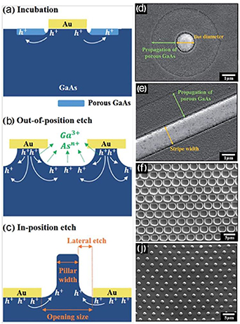
Figure 9. Schematic illustration of the three stages of metal-assisted chemical etching of GaAs: (a) incubation, (b) out-of-position, and (c) in-position of the metal catalyst. SEM images of GaAs surface topologies with Au catalysts in the form of: (d) dots (1.4 µm in diameter), (e) stripes (1.5 µm wide), after metal-assisted chemical etching and mesh pattern with metal catalyst (2 µm diameters and 2 µm space) at 45 °C (f) and 50 °C (j) for 5 min. Reproduced from [102] with permission of The Royal Society of Chemistry.
Download figure:
Standard image High-resolution imageAt a slightly increased temperature (out-of-position stage in figure 9(b)), a higher amount of holes is produced by the Au catalytic reaction. The thermal activation energy for the chemical reaction seems to remain low enough to allow mass transport of the reactants and products at the Au/GaAs interface. The created conditions lead to a faster chemical etch out-of-position of the metal catalyst, resulting in craters in the bulk GaAs with a lateral etching intrusion on the edge of the Au/GaAs interface (see figure 9(e)). At higher temperatures (in-position stage figure 9(c)), a sufficient amount of holes is generated as a result of the reaction between the metal catalyst and KMnO4 oxidant. Under these conditions, immediate metal-assisted chemical etching occurs in-position of the metal catalyst due to the rice of thermally activated chemical reactions and mass transport at the Au/GaAs interface, as shown in figure 9(d). Note that some holes may diffuse towards the bulk of GaAs leading to lateral etching out-of-position of catalytic metal. In spite of this, the authors experimentally demonstrated that the length of the lateral etch is not dependent on the opening diameters. After optimization of the etch parameters and catalyst features, high aspect ratio nano-scale pillars were fabricated.
Afterwards, the same group of authors used MacEtch for the fabrication of antireflective GaAs subwavelength structures (SWSs) [103]. The fabricated GaAs structures drastically reduced the total reflectance up to 4.5% in the wavelength range of 200–850 nm and up to the incident angle of 50° (see figures 10(a) and (b)). In their study, they demonstrated that the reflectance strongly depended on the three-dimensional features of the GaAs SWSs, which can be controlled by Au agglomeration and chemical etching. To enhance their antireflective characteristics, two wet-based etching processes, orientation dependent etching and MacEtch, were used to fabricate GaAs nano/micro dual-scale textured antireflective structures [104]. The fabricated antireflective structures presented in figures 10(c) and (d) suppressed the reflectance by the combination of the increased light absorption path in the microscale triangular structure and the increased absorption of the incident light by the continuously changed refractive index between air and GaAs in the nanohole structure.
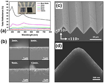
Figure 10. (a) Reflectance spectra of produced GaAs SWSs etched for 3, 6, 9, or 12 min as a function of the wavelength. Inset shows images of bare GaAs (left) and SWSs etched for 12 min (right). Reproduced from [103], Copyright (2016) with permission from Elsevier. The SEM images in cross-sectional view of GaAs SWSs for different durations of Au MacEtch are shown in (b). Reproduced from [103], Copyright (2016) with permission from Elsevier. SEM image showing tilted (c), and (d) cross-sectional views of nano/micro dual-scale textured (triangle and nanohole) GaAs fabricated by orientation-dependent etching for 25 s and MacEtch for 5 min. Reprinted with permission from [104] © The Optical Society.
Download figure:
Standard image High-resolution imageHowever, MacEtch of III–V semiconductor compounds for the fabrication of periodic nanostructures, especially in high aspect ratios, has been hardly explored in the last decade. Small microbump arrays of InP have been formed using MacEtch coupled with UV irradiation [105]. The authors described the effect of etchant concentration and catalyst species (Pt, Pd, or Au) on the resulted morphology of etched InP microstructures. They established that in the case of metal-assisted photodissolution, an exposed InP surface around a metal-coated area was etched remarkably. In addition, the etching rate of the InP substrate was affected by the difference in noble-metal species and increased in the order of Au < Pd < Pt, corresponding to the order of the magnitude of the work function of metals.
Kim et al reported fabrication of a wide variety of InP nanostructures with smooth sidewalls, lateral dimensions as low as sub-20 nm, and aspect ratio greater than 35 by a systematic inverse MacEtch (I-MacEtch) method and even without UV irradiation [106]. The term I-MacEtch is coined to describe the etching mechanism whereby a patterned metal layer acts as a catalyst as well as a mask for the formation of features in an inverse arrangement to that expected of traditional MacEtch. In this way, the I-MacEtch mechanism causes the semiconductor regions not in contact with the catalyst layer (i.e. between the metal covered areas) to be preferentially etched. In addition, the areas directly underneath the metal catalyst/mask can be etched (laterally) simultaneously at a fixed ratio relative to the vertical etch rate determined by I-MacEtch conditions. The effects of metal catalysts, nature of etching solution, etching duration, areal coverage and separation of the metal patterns, and metal pattern orientation as related to the crystallographic orientation of the substrate, on the etch rate and morphology of the resultant InP nanostructures were investigated. The SEM images of low dimensional structures (20 nm) are summarized in figure 11.
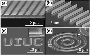
Figure 11. InP nanostructures produced via I-MacEtch: (a) arrays of nanopillars generated from Pt square pads, (b) arrays of nanoscale fins from Au lines after Au removal, (c) the letters 'UIUC' from Au pads with inset showing a high-magnification view of the outlined region (white box) corresponding to the letter 'I', and (d) concentric InP microstructures generated from a set of Au rings, with inset showing the high-magnification view of the outlined region. The inset scale bars are 500 nm. Reprinted with permission from [106]. Copyright (2015) American Chemical Society.
Download figure:
Standard image High-resolution imageThe study of MacEtch of GaN is still in the primary stage. The reported morphologies disclose mainly the pore structure [107–110]. More recently, by varying the solution composition, concentration and etch time under UV illumination, different GaN nanostructures including nanowires were reported [111–114].
Table 5 summarizes a variety of semiconductor nanostructures produced by electrochemical etching and MacEtch technologies.
Table 5. Technologies applied and parameters of the produced semiconductor nanostructures.
| Type of nano-structure | Material used | Technology applied | Parameters of the structure | Proposed application | Ref. |
|---|---|---|---|---|---|
| Triangular nanowires | Si-doped GaAs (2.7–8.6) × 1017 cm−3 | Anodization in KOH:H2O | D: 400–700 nm L: >10 µm | — | [75] |
| Nanowires | n-GaAs (0.9–2.4) × 1018 cm−3 | Anodization in HCl:H2O | D: 150–200 nm L: 100 µm | Field emission | [77] |
| Nanowires | p-ZnTe Na-doped 3 × 1018 cm−3 | Pulsed anodization in HNO3:HCl:H2O | D: 50 nm L: 10 µm | High light emission intensity | [83] |
| Nanowires | n-InP 1.3 × 1018 cm−3 | Anodization in HCl:H2O at 15 V | D: 50 nm L: 2 µm | Plasmonics | [84] |
| Nanobelts | n-InP 1.3 × 1018 cm−3 | Anodization in HCl:H2O at 13 V | Thick.: 2–5 nm Width: 50 nm Length: 2 µm | Plasmonics | [115] |
| Cone like structures | n-InAs | Pulsed anodization in H3PO4:HNO3:H2O | Height: 1 µm Top diameter: 100–200 nm | Field emission | [28] |
| Nano/micro dual scale SWS | Si-doped n-GaAs | MacEtch | Triangular- height: 8.5 µm, nanoholes: 60 nm | Anti-reflection | [104] |
| Nanowals | S-doped n-InP (0.8–8.0) × 1018 cm−3 | MacEtch | Thick.: 20 nm Height: 500 nm Length: 5 µm | Nano-electronics, opto-electronics | [106] |
2.4. Templated electrochemical deposition of metal nanowires, nanotubes and nanodots
As mentioned above, in the last decade extensive attention was paid to one-dimensional objects such as nanowires, nanotubes, and integrated arrays based on them, as they represent an emerging class of advanced multifunctional materials which are promising for wide applications in microelectronics, photonics, medicine, chemical and biological sensing. For many concrete applications, it is necessary to integrate a large amount of nanowires in one bundle or array to achieve the required functionalities.
As mentioned in the Introduction, porous semiconductors have attracted considerable interest from the point of view of manufacturing conductive nanotemplates which properties can be easily controlled by external illumination, applied electric fields, etc.
Several kinds of electrochemical deposition methods are applied for filling the pores, such as direct current electrodeposition, pulsed electrodeposition, and alternating current electrodeposition. Pulsed electrodeposition appears to be the most appropriate method for the preparation of metallic nanotubes embedded in porous semiconductor templates. It was demonstrated experimentally that in the case of macroporous Si electrochemical deposition of Cu can be realized via potentiostatic/galvanostatic electrodeposition in continuous mode, while filling the nanoscale pores in InP, GaAs or Ge require pulsed electrodeposition [116]. The possibility to deposit galvanically Ni [117] or Co [118] nanowires arrays in ultra-high aspect ratio porous InP membranes was demonstrated by coating the internal surface of the nanotemplates with a very thin dielectric interlayer prior to deposition. This dielectric layer electrically passivates the pore walls so that nucleation of metal clusters on the pore walls is prevented. At the same, time uniform distribution of Co nanodots over pore sidewall surface in the as-etched InP template was reported by Zhou et al [119].
The deposition of Pt nanotubes in InP nanotemplates (see figure 1(d)) without any passivation layer [51] was realized by electroctrochemical pulsed deposition of Pt at 40 °C for 2 h in a common two-electrode plating cell where the porous sample served as working electrode, while a platinum wire was used as counter electrode. For nanotemplates with different pore diameters, the authors used different lengths of pulses: 100 μs and 300 μs for pore diameters of 70 nm and 140 nm, respectively. A cathodic potential of −12 V was applied between the electrodes to electrochemically reduce the metal species on the surface of the porous matrix in contact with the electrolyte. To assure a uniform deposition along the depth, after each pulse a delay time as long as 1 s was used, allowing ions to diffuse into pore regions depleted during the deposition pulse. Pt electroplating in nanotemplates with pore diameters of 70 nm and 140 nm leads to uniform metal deposition on inner surface of pores along the pores (figures 12(a) and (b)). As shown in figure 12(a), many of the Pt nanotubes get out from pores and are suspended in air indicating high uniformity and strength of deposited metal nanotube in spite of the nanoscale thickness of the walls. According to [51], under a pulsed voltage regime, it is possible to control the metal deposition within limited regions in depth of the porous structures by changing the ratio between the pulse duration and delay time between pulses.
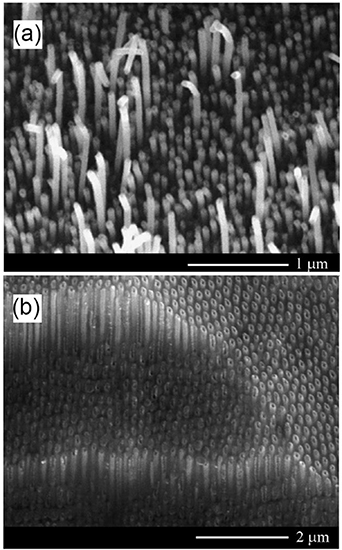
Figure 12. SEM image taken from a cleaved porous template with pore diameter 70 nm (a) and 140 nm in (b) after pulsed electrodeposition of Pt. Reprinted from [51], Copyright (2008), with permission from Elsevier.
Download figure:
Standard image High-resolution imageAn interesting issue observed is that on SEM images, the Pt nanotubes look bright in comparison with the porous n-InP skeleton walls. The metal nanotubes possess higher conductivity than semiconductor template and normally no charging phenomenon must be observed. Indeed, taking into account that pulsed electrochemical deposition of Pt on n-InP leads to the formation of Schottky barrier with the height up to 0.65 eV [120], it is obvious that the negative charge accumulates in metal nanotubes during morphology study by SEM. Using pulsed electroplating, Sato et al demonstrated uniform deposition of Pt dots with the diameters ranging from 20 to 30 nm on n-GaAs and n-InP substrates with the free electron concentrations of 2 × 10¹⁶ and 5 × 1016 cm−3, respectively [121, 122]. The authors found the Fermi-level pinning at the metal-semiconductor interface to be greatly reduced, resulting in a strong dependence of the Schottky barrier height on the metal work function.
The electronic band gap of InP is 1.3 eV at 300 K, which means that the nanotemplates based on InP are opaque in the visible region of the spectrum. Porous ZnSe templates present even more interest, since they are transparent for the visible light due to the larger bandgap of the semiconductor compound (for ZnSe e.g. = 2.7 eV at 300 K).
The electrical conductivity of ZnSe crystals can be controlled by doping and post-growth thermal treatments [123] which in turn determines the diameter of the produced pores by anodization. Figure 13(e) illustrates a porous template fabricated on 1 mm thick n-ZnSe substrate with free electron concentration of 7 × 1016 cm–3. The anodic etching was carried out in the dark at room temperature in a K2Cr2O7:H2SO4:H2O electrolyte with the ratio 5:100:10 [57]. Although the formation of uniformly distributed pores exhibiting features of short-range order is inherent to anodic etching of n-ZnSe, long-range order in pore distribution was not reached. The reason could be the absence of crystallographically oriented pores in ZnSe. As mentioned above, the long-range order in pore distribution illustrated in n-InP is favored by the network of crystallographically oriented pores initially formed in the nucleation layer [31]. In case this network is well developed, there is a general tendency of current-line oriented pores to form rows oriented along <110> direction.

Figure 13. SEM images taken from a cleaved ZnSe template with pore diameter 400 nm (a) and 40 nm (b) after pulsed electrodeposition of Pt. The insert in (a) illustrates a top view after the sample was additionally cleaved along a plane nearly perpendicular to the pores. [124] John Wiley & Sons. Copyright © 2009 WILEY-VCH Verlag GmbH & Co. KGaA, Weinheim.
Download figure:
Standard image High-resolution imagePt electroplating in pulsed voltage regime in 20 µm thick porous ZnSe layer with diameters of pores of about 400 nm and 40 nm was carried out at 40 °C for 8 h in a common two-electrode plating cell containing 2 g l−1 Pt where the porous sample served as a working electrode, while a platinum wire was used as a counter electrode. It was established that the cathodic potential depends upon the conductivity of the semiconductor template. This potential is −12 V for the used InP templates with free electron concentration of 1.3 × 1018 cm−3, −40 V for ZnSe with free electron concentration of 8 × 1016 cm−3, and −10 V for ZnSe with free electron concentration of 2 × 1018 cm−3 [57, 124]. Like in InP, after each pulse, the authors used a delay time as long as 1 sec at zero external voltage applied to allow ions to diffuse into pore regions depleted during the deposition pulse. As can be seen from figure 13(a), electrochemical deposition of Pt resulted in the formation of metal nanotubes with the wall thickness of about 50 nm. Pieces of Pt nanotubes getting out from pores are clearly seen in the cross-sectional view taken from a cleaved sample, as seen in the insert in figure 13(a). The quality of nanotubes is indicative of good uniformity of metal deposition on the inner surface of pores. The possibility of obtaining Pt nanotubes was also demonstrated for ZnSe nanotemplates with the diameters of pores of about 40 nm (figure 13(b)). Due to the small thickness of the metal wall (about 10 nm), the nanotubes can be easily destroyed – even through a simple cleavage. The high conductivity of the semiconductor nanotemplate skeleton provides conditions for uniform electrochemical deposition of metal species on the inner surface of pores, resulting in the formation of arrays of metal nanotubes embedded in semiconductor matrices.
The possibility to fabricate two-dimensional metallo-semiconductor quasi-periodic structures has also been demonstrated on porous GaP templates [125, 126]. Templates with parallel pores possessing diameters in the micrometer and sub-micrometer ranges have been fabricated by electrochemical etching of commercially available n-GaP substrates with (100) orientations and electron concentration of about 1017 cm−3 in H2SO4 aqueous electrolyte. Figure 14(a) illustrates the morphology of a porous GaP template. Similarly to InP templates, ordered arrays of pores are produced due to self-organization phenomena occurring during the pore growth. The white lines in figure 14(a) mark several directions of pore alignment in a porous GaP template. Uniform electroplating of Pt on inner surface of pores was realized in an acid platinum bath under a pulsed voltage regime, the deposition being performed at 40 °C in a common two-electrode cell where the porous sample served as a working electrode and a platinum wire was used as a counter electrode. It was found that under the pulsed voltage regime, it is possible to deposit metal within limited regions in depth of the porous structures, the depth of these regions being mainly dependent on the ratio between the pulse duration and the delay time between pulses. Electroplating starts with the deposition of metal dots, their density increasing with time. The overlapping of neighboring dots leads to the formation of tubular structures, as illustrated in figure 14(b). It was found that the application of short pulses (less than 0.3 ms) during electroplating results in a predominant deposition of Pt near the bottom of the pores, while longer pulses lead to the predominant deposition near the mouth of the pores. So, the pulse length of 0.3 ms was found to be optimal for a uniform metal deposition inside the pores of the template. As a result, arrays of metal nanotubes with the length reaching 200 μm, smooth walls and rather good mechanical strength were routinely fabricated.
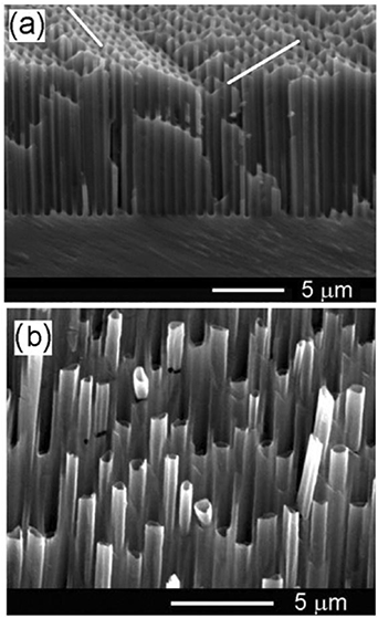
Figure 14. SEM image of a porous GaP template with ordered arrays of pores indicated by white lines (a) and an image illustrating the formation of Pt tubular structures (b). Reproduced from [125]. © IOP Publishing Ltd. All rights reserved.
Download figure:
Standard image High-resolution imageSince the GaP template is characterized by ordered arrays of pores, it was found that packs of rows of Pt nanotubes in a semiconductor envelope can be easily cleaved from the sample. In fact, the semiconductor nanotemplate with the embedded array of metal nanotubes behaves like a layered crystal, the role of individual layers being played by the rows of Pt nanotubes in n-GaP envelopes. The possibility of such a cleavage is important from the point of view of photonic applications of the fabricated metalized porous GaP templates, as discussed in section 5.
Arrays of metal nanowires and nanotubes embedded in semiconductor nanotemplates, with uniform deposition of Pt on the inner surface of pores without any activation of the pore's wall was demonstrated, regardless of the pore shape (e.g. circular, triangular-prism-like pores, etc) as shown in figure 15 [125]. Moreover, the shape of nanopores can be controlled using semiconductor crystals with different crystallographic orientations. The influence of the (100) and (111) crystallographic orientations of the n-GaP substrates upon the shape of the produced pores was reported by Schmuki et al [61, 62].
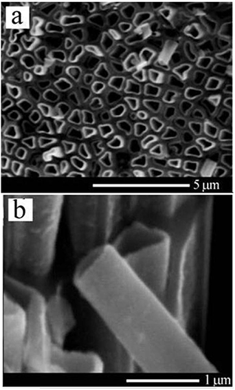
Figure 15. SEM images demonstrating formation of Pt tubular structures in GaP template with complex shapes (a) and the image of an individual Pt nanotube (b). Reproduced from [125]. © IOP Publishing Ltd. All rights reserved.
Download figure:
Standard image High-resolution imageThe electrochemical deposition of metal dots proves to be one of the most cost-effective and efficient means, especially when the dots are to be created on semiconductor substrates or matrices exhibiting electrical conductivity. The possibility to cover a huge surface inherent to GaP and InP porous structures by a self-assembled monolayer of electrochemically deposited Au nanodots was demonstrated [127]. The so-called 'hopping electrodeposition' mechanism was proposed by the authors to explain the electroplating of one monolayer of gold nanodots on porous semiconductor structures. In [125], the authors used pulsed electrochemical deposition of gold and established that after nucleation, each dot increased in size up to a critical transverse dimension of about 20 nm, the process of electrodeposition of gold being continuously supported by the formation of new nanodots. This value corroborates with the previously published data for Pt electrodeposition on n-InP, demonstrating that the value of the Schottky barrier height depends on the size of the Pt dots [121]. As the Pt dot diameter increases, the surface barrier height rapidly increases toward the value of the Mott-Schottky limit of 1.1 eV which is reached at the dot diameter of approx. 23 nm. Supposing that similar tendencies are obeyed in n-InP and n-GaP, one can expect enhanced values of Schottky barriers occurring at the interface between semiconductors involved and sub 20-nm diameter Au dots. The deposition process continues until the entire surface exposed to the electrolyte is covered by a monolayer of self-assembled gold nanodots (see figures 16(a) and (b)).
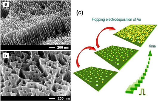
Figure 16. SEM images taken from fragments of porous GaP after electrochemical deposition of Au dots for 5 s (a) and 100 s (b). Reproduced from [127]. © IOP Publishing Ltd. All rights reserved. Schematic illustration of the 'hopping electrodeposition' mechanism is presented in (c).
Download figure:
Standard image High-resolution imageThe schematic illustration of the 'hopping electrodeposition' mechanism is presented in figure 16(c). At the beginning of electroplating the process of nucleation of gold dots takes place along with their gradual growth in size. As the transverse dimension of the dot reaches the threshold value, a Schottky barrier emerges, the barrier potential being oriented in the opposite direction relative to the applied cathodic voltage. It can be assumed that the modified local potential 'switches off' the electrodeposition within the area of this dot. To keep the process running, the system initiates the nucleation of new dots. In other words, one can imagine electrodeposition as a hopping process: Au deposition 'jumps' to other local areas as soon as one or more dots reach the threshold value of the diameter. The processes of 'switching off' and 'hopping' continue until the entire surface exposed to the electrolyte is covered by a monolayer of self-assembled Au dots. It is interesting to note that after the self-assembled monolayer is formed, further electroplating of gold is spatially non-uniform and leads to the deposition of particles with relatively large diameters.
Deposition of metal nanodots has also been investigated in porous templates with pores oriented parallel to the sample surface prepared according to a specially developed technology described in more details in section 3 [128]. A pulsed electrochemical deposition method was applied for this purpose. Figure 17(a) illustrates an InP template with pores buried underneath a thin surface layer. It was found that metal deposition takes place simultaneously both inside the buried pores and on the top template surface. On the template surface the metal is deposited in the form of nanodot lines as illustrated in figure 17(b), the thickness of such lines being determined by the number of applied pulses, while nanotubes are formed from metal nanodots inside the pores of the template as shown in figure 17(c). This uniformity of metal deposition inside the pores is ensured by the good electrical conductivity of the porous skeleton. A mechanism was discussed behind the mode of depositing nanodot lines on the top template surface and nanotubes inside the pores, on the basis of a recent work demonstrating that electroplating represents a simple and effective tool for assessing the conductivity of InP nanostructures fabricated by electrochemical etching of InP wafers [115]. The proposed approach could widen the area of potential applications of metal nanodots and nanotubes. They might be used to make plasmonic photonic crystals, optoelectronic on-chip interconnections, and chemical and biological sensors based on surface enhanced Raman scattering.

Figure 17. (a) SEM cross-sectional view of an InP template with pores parallel to the sample surface. (b) SEM view of the Au dots arrays deposited on the surface of the template after applying 100 pulses. (c) SEM image of the template with Au nanotubes deposited inside the pores, taken after removal of the surface layer of the template. The right side of the template in images (b) and (c) was protected against electrochemical deposition with the purpose of comparison.
Download figure:
Standard image High-resolution imageIt is important to note that the pulse duration and pause between pulses are the key parameters for the deposition of metal inside the porous semiconductor skeleton and for obtaining of metal nanostructures with desired shape (nanowires, nanotubes). The analysis of experimental data reveals that the pulse duration varies from 10 to 50 μs for metal nanodots formation, while the formation of metal nanotubes requires pulse duration from 100 to 300 μs and longer deposition time. At the same time, the manipulation with the amplitude of the applied pulses provides possibilities for metal deposition in a controlled fashion enabling one to reach specific designs of the semiconductor/metal porous architectures.
3. Self-organized phenomena in porous etching and formation of nanocomposite materials
3.1. Material nanostructuring by controlling the porous pattern. Pores oriented parallel to the top surface of substrates
To make use of industrial approaches of planar semiconductor technologies, it is important to develop methods for the preparation of templates with pores oriented parallel to the top surface of the substrate. These kinds of porous structures are of especial interest for the fabrication of two-dimensional and three-dimensional photonic crystals, including metallodielectric ones, since this geometry allows a wide implementation of structures due to the large surface of samples as compared to the geometry with pores propagating perpendicularly to the surface. A technological approach was elaborated by Tiginyanu et al for the preparation of porous structures with pores oriented parallel to the top surface of the substrate as illustrated in figure 18(a), taking into account that CLO pores always grow in a direction perpendicular to the equipotential lines inside the anodized sample, which means that the crystallographic orientation of the substrate does not play any role for such kind of pores, i.e. the pores look similar on (100) or (111) oriented samples [57, 129]. The method is based on a special design where some areas of the front surface of the substrate are covered by a photoresist, while other areas are exposed to the electrolyte in the anodization process. In such a case, the pores will initially grow from the surface exposed to the electrolyte in a direction perpendicular to the surface. However, with the further propagation of pores, they will be deflected in directions parallel to the top surface, and will grow under the regions covered by the photoresist. An experimental demonstration of this approach is presented for InP in figure 18(b) and for ZnSe in figures 18(c) and (d). An interesting feature of porous structures obtained by this method is the fabrication of buried porous layers, as illustrated in figures 18(b) and (c). The pores grow under a thin surface layer which remains intact during the electrochemical treatment. The thickness of this surface layer is of the order of the surface depletion region, i.e. from several tens to several hundreds of nanometers, depending on the conductivity of the anodized substrate. Figure 18(c) shows three layers present at the surface of the produced structure: a resist layer is reminiscent on a part of the sample, a virgin ZnSe layer determined by the depletion region as described above, and the porous structure buried under this surface layer.

Figure 18. (a) Illustration of the approach for the preparation of porous templates with pores parallel to the top surface of the sample. (b) SEM images of pores produced with the approach from (a) in InP (b) and ZnSe (c), (d) substrates. Reproduced from [129]. © IOP Publishing Ltd. All rights reserved.
Download figure:
Standard image High-resolution imageMoreover, this peculiarity provides conditions for reaching spectacular porous architectures by applying specially designed masks on the sample surface subjected to anodization. Recently, porous structures with the morphology illustrated in figure 19(b) were produced under square regions covered by the photoresist, separated by cross-like openings, where the sample surface is exposed to the electrolyte, as illustrated in figure 19(a) [128]. It was found that the shape of the photoresist mask determines the propagation of pores under it. If a corner of the mask is not ideally square, but rounded, the propagation of pores under this corner differs from that inherent to a sharp corner, as illustrated by the region marked with an asterisk in figure 19(b). This spectacular porous design is not only characteristic to the near-surface area, but also to the arrangement of pores in depth under the top surface, as shown in figure 19(c). The authors experimentally established that the depth of pore formation depends on the width of open windows in the photoresist deposited on the top surface, as well as on the duration of the anodization process. The mechanisms behind the formation of such porous design were disclosed, and it was proposed to use the obtained porous structures for electrochemical deposition of metallic nanostructures along predefined directions resulting in obtaining two-dimensional arrays of metallic nanotubes or nanowires embedded in semiconductor matrices, as described in section 2.

Figure 19. Schematic illustration of the used mask design for anodization: (a) SEM images of porous InP after anodization through open windows in the photoresist, (b) top view under the photoresist, (c) cross-sectional tilted view of (b).
Download figure:
Standard image High-resolution imageTo achieve lateral etching, Yang et al proposed to use a laser scribing (LS) process in GaN epilayers instead of using photoresist masks [130]. To expose the side walls of the n-type GaN layer, parallel etching channels with a 300 µm-spacing were defined using the laser scribing, as shown in figure 20(a). It was shown that the cross-sectional shape of pores produced by lateral anodic etching after the LS process can be tailored from triangular pores to highly parallel quasi-circular pores by increasing the anodic voltage. The produced well-ordered laterally mesoporous GaN proved to be suitable for the enhancement of water splitting performance of GaN photoanodes, as well as for the development of high-detectivity ultraviolet photodetectors, as described in section 5. Another composite porous GaN structure for water splitting was designed and fabricated on the basis of laterally porous GaN, with an additional inductively coupled plasma (ICP) etching process of the top surface to produce hexagonal hole arrays through an AAO membrane [131]. A design with both well-ordered lateral and vertical holes was obtained with this combined process. Possibilities to fabricate parallel aligned mesopore arrays in pyramidal-shaped GaN were demonstrated by making use of electrochemical anodic etching techniques, followed by similar inductively coupled plasma etching, but assisted by SiO2 nanosphere lithography instead of an AAO membrane [132].
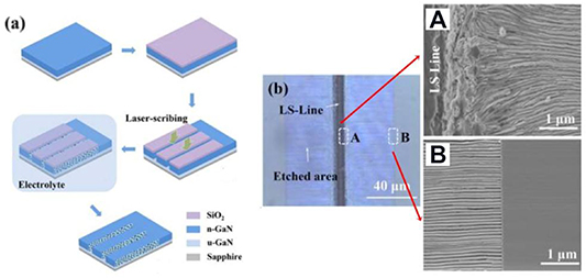
Figure 20. (a) Illustration of the process diagram for the laterally etched porous GaN: epitaxial growth of GaN; deposition of SiO2; laser scribing for the etching channels; anodic etching; removal of SiO2. (b) The micrograph of the laterally porous GaN etched at 15 V for 5 min. Top-view SEM images of (b) at the pore initiation (A) and the pore tip (B), respectively. Reprinted with permission from [130]. Copyright (2017) American Chemical Society.
Download figure:
Standard image High-resolution image3.2. Multilayer porous structures
The possibilities to fabricate self-organized two-dimensional (2D) hexagonal arrays of pores in semiconductor compounds using electrochemical etching techniques were mentioned in section 2. Interesting morphological properties have been reported on III–V materials over the last decade. Many groups focused their research on finding the way to induce periodicity in the third direction, making semiconductor nanotemplates prospective for applications as photonic crystals. Two different ways were proposed to solve this issue: (a) modulation of the diameter of the current line oriented pores for a certain length, similarly to Si, and (b) switching periodically the pore growth from current line oriented pores to crystallographically oriented pores. In the first case, the modulation of the pore diameter occurs due to self-induced voltage oscillations inherent to the electrochemical etching process [133]. It was found that the system has an internal time constant, and the internal oscillation frequency changes with growing the pores into the substrate. As a result, the modulation uniformity of the pore diameters changes as the pores grow into the substrate. In order to obtain a uniform modulation of the pore diameters over the whole depth of the structure, it was proposed to apply externally modulated current densities at different frequencies, and to change the frequency in time, i.e. a higher frequency at the beginning and a lower frequency at the end of the experiment.
The best morphology control is provided by switching between current line oriented pores and crystallographically oriented pores, realized with anodization in a pulsed mode composed of two phases: phase 1 with high voltage/currents and duration of Δt1, and phase 2 with low voltage/currents and duration Δt2. The crystallographically oriented pores are obtained in low voltage/current experiments. These type of pores have three important anisotropic characteristics: growth along <111> B directions, a triangular shape, and quite a low growth rate (~ 1 μm min−1). In high voltage/current experiments, current-line oriented pores start to grow perpendicular to the equipotential lines in the substrate and reach growth velocities up to 30 μm min−1. Switching between current line oriented pores and crystallographically oriented pores was demonstrated by the anodization of InP samples in the pulsed mode [133]. A structure obtained in the galvanostatic anodization process, as a result of a periodic switch from 600 mA cm−2 (Δt1 = 0.1 min) in the first phase to 0 mA cm−2 (Δt2 = 0.5 min) in the second phase, is illustrated in figure 21(a). The morphology of the structure is characterized by a stack of porous layers with different degrees of porosities and, consequently, with different effective refractive indices.
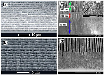
Figure 21. Multilayer porous structures in InP (a) smooth structure obtained by switching the current from 600 mA cm−2 (phase 1, Δt1 = 0.1 min) to 0 mA cm−2 (phase 2, Δt2 = 0.5 min). (b) waved structure, phase 1, U = 7 V, Δt1 = 0.04 min, phase 2, U = 1 V, Δt2 = 1.5 min). [133] John Wiley & Sons. Copyright © 2005 WILEY-VCH Verlag GmbH & Co. KGaA, Weinheim. ZnSe (c) tree porous layers with different degrees of porosity, as well as (d) two porous ZnSe layers demonstrating formation of large pores at high applied voltage (15 V) in the upper layer and porosification of the thick pore wall by successive anodization at lower applied voltage (8 V) concomitantly with the formation of the second lower layer with small pores. [124] John Wiley & Sons. Copyright © 2009 WILEY-VCH Verlag GmbH & Co. KGaA, Weinheim.
Download figure:
Standard image High-resolution imageThe morphology will look totally different in the case of the potentiostatic anodization process with applying a high voltage in the first phase and a low voltage in the second phase. An example of such morphology is illustrated in figure 21(b). As it can be observed, also in this case, switching from crysto to curro pores occurs, however, it does not result in a smooth transition between the two layers as in figure 21(a), but a wavy interface is encountered. A model mechanism for obtaining such wavy morphology was proposed, taking into account the peculiarity of crysto and curro pores growing. Therefore, photonic crystal structures with different dimensionalities can be produced by making use of either galvanostatic or potentiostatic pulsed anodization modes.
In spite of the fact that the growth of crysto pores was not observed in ZnSe, underlying the absence of long-range order pore distribution, pore rows oriented along the <110> direction were realized as can be seen from the arrow in the inset of figure 21(c), and the fabrication of multilayer porous structures with different degrees of porosity was demonstrated in figure 21(c) [124]. However, the formation of layers with different degrees of porosity is due to the growth of pores with different transverse sizes at different applied voltages in this case, in contrast to switching between crysto and curro pores realized in InP substrates. Another peculiarity of the successive anodization of ZnSe substrates at varied applied voltage is the porosification of the same layer at two different length scales, shown in figure 21(d), which opens new possibilities for the design and fabrication of devices based on porous semiconductor compounds.
Self-organized processes were also shown to represent a basis for the fabrication of multilayer porous structures in HVPE grown GaN [134, 135]. As already mentioned in section 2, the fine modulation of the electrical and optical properties, both in-depth and in-plane directions, within extended areas, was found to be one of the peculiarities of HVPE growth of bulk GaN [136–138]. It was demonstrated by Kelvin Probe Force Microscopy and by SEM mapping after electrochemical etching [44], as well as by photoluminescence analysis [139], that this fine modulation of the electrical conductivity, determining the creation of self-organized 3D nanostructured architectures, including quasi-ordered concentric hexagonal structures, is related to the self-organized spatial distribution of impurities generated during the growth of single crystalline n-GaN substrates by HVPE. A model has been proposed to explain the formation of these self-organized spatial architectures on the basis of generation of V-pits and their subsequent overgrowth accompanied by the growth in variable direction. These peculiarities of the HVPE growth were used to prepare multilayer porous structures by electrochemical etching, as demonstrated in figure 22(a), since the resulting porosity is a function of carrier concentration in the respective layer, as discussed above. The formation of multilayer porous structures was investigated as a function of the voltage applied during the electrochemical etching, the electrolytes used, and the duration of the etching process.
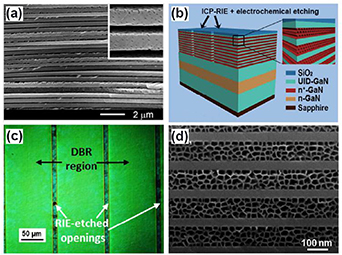
Figure 22. (a) SEM image taken from a cleavage plane of a HVPE-grown sample subjected to electrochemical etching in 0.3 M HNO3. Inset is the enlarged view of an area with the size of 1 × 1 μm2. Reprinted from [134], Copyright (2017), with permission from Elsevier. (b) A schematic process flow of forming highly reflective DBR mirror with NP-GaN layers via lateral etching of highly doped sidewalls trough opened trenches. (c) Top-view optical micrograph showing openings created by ICP-RIE (dark green regions labeled by white arrows) and the highly reflective GaN/NP-GaN DBR regions (light green regions labeled by black arrows). (d) A zoomed-in cross-sectional SEM image of a GaN/NP-GaN DBR structure. Reprinted with permission from [140]. Copyright (2003) American Chemical Society.
Download figure:
Standard image High-resolution imageHowever, while these self-organized processes are useful for the preparation of multilayer porous structures, they are not totally under control. A better control of the multilayer design from the point of view of electrical conductivity of layers is ensured by the MOCVD-growth of GaN. Multilayer structures grown by MOCVD and porosified by electrochemical or photoelectrochemical etching were widely used for the fabrication of distributed Bragg reflectors, as discussed in section 5 [134, 140–142].
A representative process flow for the fabrication of DBR mirrors on MOCVD grown GaN by electrochemical etching is shown in figures 22(b)–(d). This flow includes: (i) growth of an epitaxial structure consisting of alternating n+-GaN/GaN layers; (ii) lithographical patterning with trenches created by inductively coupled plasma reactive-ion etching (ICP-RIE, via windows) to expose the sidewalls of the alternating layers, since the EC etching is designed to proceed laterally; (iii) covering the top of the sample surface by SiO2, while the edge is connected to a source meter to apply the anodic bias; and (iv) EC etching for the lateral porosification of the exposed sidewalls in the direction perpendicular to the sidewall.
However, this process flow has some drawbacks. Due to the fact that the electrochemical etching process is limited in the lateral direction, the sample has to be patterned into ~50 µm trench openings, which is detrimental to practical optoelectronic devices applications on a large scale. Apart from that, the top GaN surface has to be protected by a thick silicon dioxide layer, which induces additional processing steps and constrains the material design. In order to overcome these drawbacks, a facile wafer-scale (2-inch) fabrication route was proposed that utilizes a one-step selective electrochemical porosification of highly silicon doped GaN layers, which occurs both laterally and vertically [142]. This route does not involve any additional SiO2 layer deposition to protect the top GaN surface and no extra processing/masking is needed for the subsequent electrochemical etching process, which results in a much simplified fabrication process.
3.3. Formation of single crystals of pores
The obtained multilayer Bragg structures represent 1D photonic crystal structures. Generally, a 1D photonic crystal is a periodic stack of thin dielectric films with two different refractive indices n1 and n2. Similarly to usual electronic crystals formed by a periodicity of potential and characterized by the energy bandgap, the photonic crystals exhibiting a periodic modulation of the refractive index are characterized by photonic bandgaps. The two important geometrical parameters determining the wavelength of the photonic bandgap for a 1D photonic crystal are the lattice constant a = d1(n1) + d2(n2) and the ratio of d1 to a, where d1,2 is the thickness of the layer with refractive index n1,2 . In the case of 2D photonic crystals, the concept is extended to either air holes in a dielectric medium or dielectric rods in air. Therefore, ordered porous dielectric materials, including porous semiconductors with parallel pores, are intrinsically 2D photonic crystals. However, for the purpose of obtaining a 2D photonic crystal, one needs to have a highly ordered arrangement of pores or, in other words, to have a 2D single crystal of pores.
There are different ways to produce a single crystal of pores. For instance, they are easily produced in Si and Al2O3 with lithographical prepatterning. On the other hand, generating lithographically produced nucleation sites on III–V compounds is possible, but not quite as easy as on Si (and much more expensive and harder to obtain). Anyway, single crystal of pores was demonstrated in III–V compounds without prepatterning, due to the above discussed self-organized processes and self-induced voltage oscillations inherent to the electrochemical etching process [31, 143–146].
It was shown that 2D pore crystals in III–V compounds require either samples oriented in (111B) or the formation of curro pores. To reach the growth of ordered crysto pores in <111> B directions is rather difficult due to random nucleation. On the other hand, for relatively large current densities, curro pores that exhibit a strong tendency to form a close packed arrangement with lattice constants ranging from 50 nm to 2 µm and typical dimensions of a few lattice constants with short-range order can be easily obtained in InP. Moreover, upon optimizing the etching conditions, in particular with respect to the voltage, long range order may evolve, leading to the formation of a single crystal of curro pores (figures 23(a) and (b)).

Figure 23. (a) Ordered distribution of CLO pores in n-InP with lattice constant of a ≈ 200 nm after the nucleation layer has been mechanically removed. (b) The same but with lattice constant of a ≈ 800 nm. [145] John Wiley & Sons. © 2003 WILEY-VCH Verlag GmbH & Co. KGaA, Weinheim.
Download figure:
Standard image High-resolution imageAs to the 3D pore crystals, they can be fabricated either from 2D pore crystals by pore diameter modulation in the third dimension, or by growing cristo pores in specific crystallographic directions. For instance, in n–type silicon wafer with (100) orientation, the pore diameter of the macropores can be modulated in depth during the fabrication process by modulating the intensity of the back side illumination of the wafer. Strong illumination leads to high etching currents and, therefore, wide pores while the opposite is valid for low illumination. Figure 24(a) shows a SEM image of a longitudinal section of an Si sample. Self-induced phase-coupled diameter oscillations of pores occur also in n-InP (figure 24(b)), and they are accompanied by external voltage oscillations if the etching is performed under constant current conditions [143]. With a strong degree of self-organization inherent to InP, by means of external modulation of the pore diameter during the growth of a 2D pore crystal, it was possible to obtain a completely self-organized 3D crystal, as shown in a collage giving some perspective in figure 24(d).
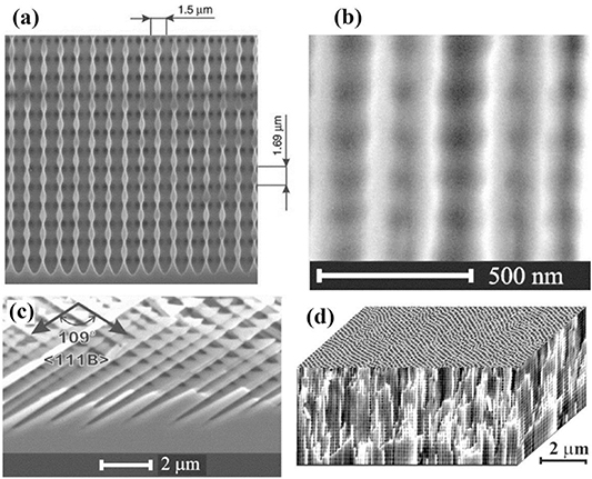
Figure 24. (a) SEM–image showing a longitudinal section of the modulated pore structure in macroporous Si. Reprinted from [147], with the permission of AIP Publishing. (b) Current line oriented pores in InP, cross-section with diameter oscillations. Reprinted with permission from [143] COPYRIGHT: © Materials Research Society 2002. (c) Crystallographically oriented pores in (100)-oriented n-GaAs. [31] John Wiley & Sons. Copyright © 2003 WILEY-VCH Verlag GmbH & Co. KGaA, Weinheim. (d) 3D single pore crystal obtained by self-organization. Reprinted with permission from [143] COPYRIGHT: © Materials Research Society 2002.
Download figure:
Standard image High-resolution imageAnother way to obtain a 3D crystal of pores is to make use of growing cristo pores in specific directions, as shown in figures 1(a) and 24(c). In contrast to (100) Si wafers, on (111) wafers, <100> pores would grow under an angle of 54° to the normal. In this configuration, the second slowest passivated direction <113> with an angle of 34° governs the pore growth [147]. At the nucleation points on the surface, tripods consisting of three equal <113>-directions begin to grow. They form an interpenetrating network of pores. If pores are grown with lithographically defined nucleation spots, a Yablonovite–like structure is found [148]. This structure represents an orthorhombic crystal, which according to calculations, will produce a full photonic band gap. However, up to now, lithographically prestructured samples have not yet reached optical quality.
Instead of employing the crystallographic equivalence of three <113> directions of (111) oriented samples in Si, one can employ four <111> directions in (100) oriented III–V compounds. However, a full 3D structure with an interpenetrating network of pores in four <111> directions would produce a cubic structure which most likely does not exhibit a photonic band gap in all directions [143]. Moreover, the research has shown that pores will only grow in the two <111> B directions in III–V compounds, and the photonic properties of the subset with pores only in two of the four <111> directions are not clear at present.
3.4. Nanocomposite materials based on porous semiconductors
Porous materials are intrinsically suitable for the preparation of nanocomposites by filling them with various substances. Even without any filling, the porous materials represent composites, since they are formed by two constituents: the skeleton of the basic material and the pores filled with air. In the case of semiconductor compounds, the composition of the porous skeleton can be varied, the main attention so far being paid to III–V and II–VI compounds. As concerns the substances introduced in pores, filling them with rare earth elements was widely focused on due to attempts to prepare media for optical nanodevices, including media with controlled light scattering properties for the development of random lasers, as described in section 5 [149–151].
Apart from wide-bandgap semiconductors transparent to visible light, porous templates like GaAs and InP are of interest for doping with rare-earth ions exhibiting intrashell transitions in the IR spectral range, e.g. the 1500 nm transition in Er3+ ions which is a popular choice in a wide variety of telecommunication applications. Moreover, the easy oxidation of semiconductor templates results in nanostructured oxides which are the most commonly used materials in phosphor technologies.
The technology for the doping of porous semiconductor compounds like GaP, InP, and GaAs with rare earth elements implies impregnation of Eu or Er ions form EuCl3:C2H5OH and ErCl3:C2H5OH solutions followed by thermal treatment in the temperature interval from 500 °C up to 1000 °C to activate the introduced ions. However, it was found that simultaneously with the activation of the rare earth ions, oxidation of the semiconductor skeleton as well as the formation of a variety of rare earth related compounds occurs under annealing at high temperatures, while the volume ratio of the obtained composite material components is highly impacted by the concentration of the impregnation solutions used, the annealing temperature and the duration of thermal treatment. In order to inhibit and easily control the oxidation of the porous template it was proposed to perform the annealing in nitrogen flow containing less than 1% oxygen. The conditions of thermal treatment also determine the crystallographic structure of the native oxides formed and that of rare earth compounds [152].
The oxide component produced in GaP porous templates was identified as GaPO4 in two modifications: α-quartz type structure, or low-cristobalite phase, depending on the conditions of the thermal treatment, while the oxide obtained in GaAs porous templates is related to the β-Ga2O3 phase.
Both compositions of the EuAsO4 and ErAsO4 micro crystallites produced in the GaAs templates were of xenotime-type, while in the case of GaP templates the EuPO4 crystallites were of monazite-type and ErPO4 crystallites exhibited a xenotime structure. Figure 25 illustrates the morphologies, compositions and crystallographic structures obtained in GaP porous templates impregnated with Eu and Er solutions. In a porous GaP layer with the characteristic size of the skeleton comparable with the diameter of pores, the oxidation proceeds at high annealing temperatures with the formation of micromatch heads (figure 25(b)). By increasing the annealing time, the micromatch heads merge with each other, resulting in the formation of microwormlings (figure 25(a)). At long annealing times, an oxide columnar-lamellar nantostructure is formed underneath the cap oxide layer, as shown in figure 25(c). As concerns the GaPO4 oxide, a hexagonal P3121 α-quartz type phase was obtained with slow cooling after annealing (curve 1 in figure 25(d)), while an orthorhombic C2221 low-cristobalite structure was produced with fast cooling (curve 2 in figure 25(d)). The monazite EuPO4 and xenotime ErPO4 phases are shown in figure 25(e).

Figure 25. Morphologies of oxide structures formed in GaP templates: (a) top view; (b) cross-section of the cap layer; (c) the underneath structure (c). (d) The XRD pattern of the GaPO4 oxide produced by annealing porous GaP layers at 900 °C during 30 min followed by slow cooling (1) and fast cooling (2). (e) The crystallographic phases of a nanocomposite prepared on GaP templates infiltrated with EuCl3:C2H5OH (3) or ErCl3:C2H5OH (4) solutions and annealed at 800 °C. [152] John Wiley & Sons. Copyright © 2009 WILEY-VCH Verlag GmbH & Co. KGaA, Weinheim.
Download figure:
Standard image High-resolution imageThe produced nanocomposite materials are characterized by bright luminescence coming from intrashell transitions in rare earth elements incorporated in various nanophases. The nanocomposites doped with Eu exhibit three red complex PL bands in the region of 580–600 nm, 610–620 nm and 680–700 nm related to 5D0 → 7F1, 5D0 → 7F2, and 5D0 → 7F4 intrashell transitions, respectively. The structure of these complex bands is determined by the site occupied by the Eu3+ ion in nanophases of the nanocomposite. The green luminescence in the region of 540–555 nm is predominant in nanocomposites doped with Er, and it comes from 4S3/2 → 4I15/2 intrashell transitions in the Er3+ ions. Analysis of the luminescence intensity under excitation by different laser lines showed that the highest luminescence intensity from samples doped with Er is observed under excitation by the 488.0 nm laser line, while in Eu doped samples, this is achieved under the excitation by the 465.8 nm laser line. Since the prepared composite materials are transparent for visible and UV light, it was suggested that they may find applications as light emitters for integrated optoelectronic and photonic circuits. It was also proposed to use this composite in the design of multiphase random laser media in which the high-index semiconductor skeleton provides strong light scattering necessary for the formation of random laser cavities, while the oxide rare-earth-doped phase plays the role of emitting and amplifying the electromagnetic radiation, as described in section 5.
A high optical quality ZnO material was produced from bulk ZnSe wafers subjected to thermal treatment in an oxygen containing atmosphere [153], as shown in figure 26. It was shown that the obtained material can act as a gain medium for stimulated emission in the ultraviolet spectral region, while the morphology of the nanostructured material with the mean size of grains between 100 and 200 nm (figure 26(a)) is suitable for random laser action. Even more possibilities for the control of morphology, and, respectively, the light scattering properties, which are important for random laser action, are provided by the preliminary preparation of porous ZnSe templates (figure 26(b)), which are subsequently transformed into porous ZnO templates (figure 26(c)) by thermal treatment. The gradual transformation of the crystal structure and the luminescence properties of the produced composite material as a function of the annealing temperature are illustrated in figures 26(d) and (e), respectively.

Figure 26. (a) SEM image taken from a nanostructured ZnO sample produced by annealing of bulk ZnSe, (b) ZnSe template produced by electrochemical etching. (c) A nanostructured ZnO template produced by annealing of a ZnSe template. (d) XRD spectra of a ZnSe wafer (1) and of the material produced by annealing of this wafer at 600 °C (2) and 800 °C (3). (e) Photoluminescence spectra of a ZnSe wafer (1) and of the material produced by annealing of this wafer at 600 °C (2) and 800 °C (3). Spectra (2) and (3) are multiplied by 20 and 2000, respectively, for a shift along the logarithmic intensity axis for the sake of clarity. Reproduced from [153]. © IOP Publishing Ltd. All rights reserved.
Download figure:
Standard image High-resolution imageThe suitability of the GaN nanoporous templates for the preparation of composite materials was also demonstrated via their infiltration with methylammonium lead bromide perovskite (CH3NH3PbBr3, or MAPbBr3) [154]. Halide perovskites hold exceptional promise as cheap, low temperature solution-processed optoelectronic materials. However, their poor structural and chemical stability when exposed to moisture or air is an essential drawback. The proposed procedure for infiltration into nanoporous GaN proved to be a good solution for these problems. The protective effect of the GaN porous template was demonstrated by the preservation of the green photoluminescence of the perovskite after up to 1 year of storage under ambient conditions. It was suggested that the proposed method may be generalized to related perovskite materials, offering a route to fabricating composites of interest for use in various optoelectronic devices.
4. Properties of porous semiconductor compounds
4.1. Photo- and cathodoluminescence
The luminescence properties of porous semiconductors could be influenced by quantum size effects, i.e. the band-edge emission may be shifted to higher photon energies with respect to the bandgap energy of the bulk material [155–160]. In the case of strong quantum confinement, the semiconductors with the bandgap energy in the infrared spectral region exhibit visible luminescence after porosification. However, the characteristic sizes of the pore walls should be smaller than the exciton Borh radius, in order for such effects to be observed. Usually, the Bohr radius of excitons is of the order of 2–10 nm, except for narrow bandgap materials, such as InAs, InSb, etc, for which the value is of several tens of nm. On the other hand, at larger dimensions of the porous skeleton, where quantum size effects are not expected, a clear correlation between the morphology and the cathodoluminescence (CL) characteristics of porous layers obtained by electrochemical dissolution of n-GaP and n-InP substrates was disclosed. However, the effect of porosification upon the emission intensity could be different for different materials.
The morphology of porous layers produced by electrochemical treatment in acidic solution is determined by the anodization conditions applied, thus providing opportunities for controlling the spatial distribution of emission in porous layers, which was demonstrated for GaP [161, 162] and InP [162]. A quite different impact of porosity upon CL efficiency was observed at high and low anodic current densities in GaP. Particularly, it was found that anodization at high current densities (e.g. 100 mA cm−2) sharply enhances the CL intensity, while etching at current densities as low as 1 mA cm−2 quenches the luminescence, as shown in figure 27(a). In contrast to this, anodization at both high and low current densities leads to the decrease of CL intensity in porous InP layers, as compared to the bulk material, illustrated in figure 27(b). The chemical composition microanalysis proved the stoichiometry of porous GaP and InP structures fabricated at both low and high anodic current densities. The variations in CL intensity were explained in terms of different levels of passivation of the pore walls surfaces depending on the technological conditions of anodization. In this case, when self-induced voltage oscillations occur during anodic etching, they lead to modulation of the degree of porosity, and, respectively, to modulation of the CL intensity.
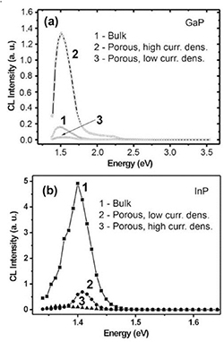
Figure 27. (a) CL spectra of bulk GaP (curve 1) and porous layers produced at current densities of 100 mA cm−2 (curve 2) and 1 mA cm−2 (curve 3). (b) CL spectra of bulk InP and porous layers produced at high current densities (curve 2) and low current densities (curve 3). Reproduced with permission from [162] © EDP Sciences, 2004.
Download figure:
Standard image High-resolution imageInvestigations of photoluminescence in porous InP structures prepared in a neutral NaCl electrolyte also showed a decrease of the luminescence intensity in the porous material as compared to that inherent to the bulk one [52]. However, the decrease is only by a factor of 3–4, as compared to orders of magnitude decrease in porous samples prepared in acidic electrolytes. Therefore, the decrease is not so significant in porous samples prepared in the neutral NaCl electrolyte, if the huge internal surface of the porous skeleton is taken into account. It was concluded on the basis of these observations that anodization in NaCl electrolytes leads to effective passivation of the porous sample surface as compared to anodization in acid electrolytes.
Similarly to the case of InP, the suppression of the near-band-edge (excitonic) emission was evidenced in other direct bandgap materials (CdS and CdSe) subjected to photoelectrochemical etching, which resulted in the formation of a porous fractal-type morphology [163]. Apart from the suppression of the excitonic emission, the emergence of dipper and broader PL band was observed in these materials after photoetching in acidic solution. A decrease by more than two orders of magnitude of the excitonic emission was also found in porous CdSe layers produced by photoelectrochemical etching in HCl aqueous solutions, these layers with uniform porosity being composed of pores with diameters of about 200 nm stretching perpendicularly to the initial surface of the sample [164]. The phenomenon of effectively inhibited luminescence was attributed to the enhanced surface recombination in the porous matrix characterized by high surface-to-volume ratio. A comparison of the effects of porosity on photoluminescence intensity in different materials is summarized in table 6.
Table 6. The effect of photoelectrochemical etching upon the luminescence efficiency of porous materials.
| Material | Ratio of the luminescence intensity in porous to bulk material | Ref. |
|---|---|---|
| GaP | 6 | [161, 162] |
| InP etched in acidic electrolyte | 10–2 | [162] |
| InP etched in neutral NaCl electrolyte | 0.3 | [52] |
| CdSe | 0.3x10⁻² | [164] |
| ZnSe pore size ~50 nm | 0.4 | [165] |
| ZnSe pore size ~ 500 nm | 2.3 | [165] |
Taking into account that GaP doped by nitrogen as well as GaP doped by zinc and oxygen are used in the development of yellow-green and red LEDs, respectively, some properties of porous GaP could be useful for the improvement of parameters of devices. However, this issue needs deep investigation to demonstrate that, when applied to specifically doped GaP, porosification has no adverse effects on characteristics of LEDs. On the other hand, surface passivation methods should be elaborated for such materials as InP, CdS, CdSe and others. From this point of view, porosification in neutral NaCl electrolyte is preferential, since it leads to surface passivation during electrochemical etching. However, the degree of passivation is still not enough, the luminescence from porous layers being less intense as compared to that from the bulk material.
As described in section 2, in contrast to the uniform porosity generated by photoelectrochemical etching, anodization of CdSe in the dark leads to the formation of porous layers exhibiting pronounced fluctuations in the spatial distribution of the density of pores, and to the formation of porous domains with a much higher density of pores as compared to other regions of the porous structure (see figure 2) [32]. These domains are formed due to nonuniform nucleation of pores at the initial surface of the sample, and due to peculiarities of further pore propagation underneath the sample surface. Especially strong scattering of light occurs in regions with high porosity, which ensures the formation of closed loop paths for the light through multiple light scattering. It was shown that the architecture of the porous network may generate a huge amount of closed loop paths, and the regions with high porosity play the role of ring microcavities for light, which may lead to the occurrence of lasing effect. Figure 28 illustrates the PL spectrum of porous CdSe regions exhibiting strong scattering of light (curve A), as compared with the luminescence from the bulk CdSe (curve B), and the porous sample with a uniform distribution of pores, fabricated under in situ illumination (curve C). The emergence of the broad band emission depicted by curve A exhibited a threshold behavior, namely the PL was totally quenched at the excitation power densities lower than 300 W cm−2, while the integrated emission intensity sharply increased with the excitation power density (Jex), in accordance with the relation IPL ∼ (Jex)5. This fascinating effect of the gain of luminescence was attributed to the amplification of the emission in ring microcavities inherent to porous CdSe areas characterized by strong light scattering, while the broadness of the spectral emission from these areas was attributed to statistical size distribution of ring microcavities occurring in the porous network. These observations pave the way to the design and fabrication of random lasers based on semiconductor materials.
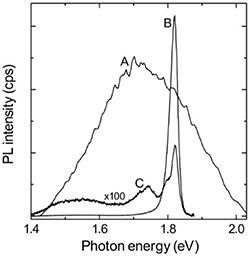
Figure 28. PL spectra of porous CdSe regions exhibiting strong scattering of light (curve A), bulk CdSe (curve B) and porous CdSe fabricated under in situ illumination (curve C). Excitation power density (W cm−2): curve A, 103; curves B and C, 3 × 10². Reproduced from [32]. © IOP Publishing Ltd. All rights reserved.
Download figure:
Standard image High-resolution imageAs concerns GaN, it was shown that the luminescence of porous GaN structures can be controlled by the conditions of photoelectrochemical etching in a 4.6 M HF aqueous solution, particularly by the duration of the etching process [41]. In all porous samples, the PL intensity is higher as compared to that inherent to the bulk material. Initially, the PL intensity increases with increasing the etching time up to 20 min, while afterwards, however, the PL intensity decreases with the etching time. Therefore, the sample etched for 20 min exhibits the highest peak intensity, which is an order of magnitude higher as compared to the bulk material. This effect was explained by the enhancement of light extraction efficiency in porous structures, due to the larger surface-to-volume ratio in the etched samples, which can increase the contact area between GaN and excitation light, while the sidewalls of porous GaN contribute to the light scattering to increase the number of emitted photons.
A similar phenomenon was observed in porous GaN fabricated by photoelectrochemical etching in 1-ethyl-3-methylimidazolium [EMIM] trifluoromethanesulfonate [OTF]-based ionic liquids [42]. In this case, it was found that the highest peak intensity (one order of magnitude higher as compared to the bulk material) is reached in samples etched for 1 min (figure 29).
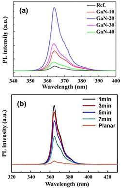
Figure 29. (a) PL spectra of the as-grown and GaN etched in 4.6 M HF aqueous solution for 10, 20, 30, and 40 min. Reprinted from [41], Copyright (2018), with permission from Elsevier. (b) PL spectra of the as-grown and GaN etched in [EMIM]-[OTF]-based ionic liquids for 1, 3, 5, and 7 min. Reprinted from [42], Copyright (2018), with permission from Elsevier.
Download figure:
Standard image High-resolution imageApart from that, a gradual blue shift of the PL peaks of the etched GaN was observed with increasing the etching time, as compared to that of the as-grown GaN, which was explained by the relaxation of compressive stress induced by etching [41]. It was shown that there exists an optimum pore structure assuring PL performance, which demonstrates that the fabricated porous GaN structures have great potential for a series of optical devices.
The PL investigations in various porous GaN samples also revealed the porosity-induced quenching of luminescence bands related to several structural defects induced by strains in bulk GaN. This quenching effect is related to the relaxation of strains in porous samples [166]. Apart from the relaxation of strains, porosification can also be used for preferential etching of dopant atoms (vacancies) near the semiconductor surface, as shown for n-CdSe samples. It was shown that the doping density can be reduced near the semiconductor surface by one order of magnitude, after photoetching [167, 168]. It was suggested that the photoetching of II–VI compounds can be useful for creating profile of donors which is desirable for optoelectronic devices [168].
In addition to the technological parameter of photoelectrochemical etching time duration, the current density during the etching process is another parameter which can be used for controlling the degree of porosity and the luminescence intensity in porous GaN samples. It was found that the photoluminescence intensity increases with the increase of the current density during the photoelectrochemical etching of GaN. The room temperature near band-edge PL peak intensity of porous samples has increased by more than one order of magnitude compared to that of the as-grown one, at an optimum current density [169, 170].
Therefore, the current density and the duration of photoelectrochemical etching are important technological parameters for the optimization of the luminescence intensity in porous GaN structures. However, the type of the electrolyte used also influences the luminescence intensity. A comparative study of the impact of the electrolyte on the properties and the behavior of GaN during the photoelectrochemical etching process performed with four different electrolytes revealed that the enhancement of the PL intensity of the porous GaN strongly depends on the electrolytes [171]. PL intensity is higher for samples etched in H2SO4:H2O2 and KOH as compared to samples etched in HF:HNO3 and in HF:C2H5OH. The PL intensity of samples etched in H2SO4:H2O2 was found to be higher by a factor of more than 20 as compared to that inherent to the bulk material [172].
The influence of the electrolyte used for porosification of GaN upon the luminescence efficiency is illustrated in table 7.
Table 7. The effect of photoelectrochemical etching of GaN in different electrolytes on the luminescence efficiency of the porous material.
| The GaN material | The electrolyte used | Ratio of the luminescence intensity in porous to bulk material | Ref. |
|---|---|---|---|
| HVPE-grown, Si-doped, electron conc. 4 × 1018 cm−3 | HF | 10 | [41] |
| HVPE-grown, Si-doped | EMIM-based ionic liquid | 9 | [42] |
| Unintentionally doped n-GaN, electron conc. 2.3 × 1017 cm−3 | KOH | 1.6 | [166] |
| MOCVD-grown, Si-doped, electron conc. 4 × 1018 cm−3 | HF-ethanol | 13 | [169] |
| MBE-grown, electron conc. 2 × 1019 cm−3 | HF-ethanol | 22 | [170] |
| MOCVD-grown, Si-doped, electron conc. 1 × 1017 cm−3 | HF-ethanol HF-HNO3 KOH H2SO4-H2O2 | 1.3 4.5 13.8 23.7 | [171] |
It can be seen from table 7 that the photoluminescence enhancement in porous GaN is even higher than that observed in porous GaP. As already mentioned in relation to the possibilities to use the enhanced luminescence properties of GaP for the development of LEDs, this issue also needs a systematic study in GaN, especially taking into account that GaN is a direct bandgap material, while investigation of the influence of porosification on its properties started much later as compared to GaP. In particular, it should be demonstrated that the enhancement of luminescence properties after porosification can also occur in high quality GaN used in LEDs. Nevertheless, even having no definite answer to this question currently, introducing porosity in semiconductors proved to be useful for the development of light emitting devices by employing other aspects of porosification, as described in section 5.
A detailed investigation of the optical properties of porous GaN films with different porosities revealed that the enhancement of excitonic emission in porous samples is related to the local concentration of the electric field at GaN nanoparticles and pores due to the depolarization effect, as well as to the efficient light extraction from the porous skeleton. The light extraction efficiency and the suppression of non-radiative recombination channels are promoted by the large surface of the air/semiconductor interface. It was suggested that introducing porosity is an efficient way to increase the emission efficiency of nanophotonic devices based on porous GaN [173].
The enhancement of PL intensity and strong release of stress was also observed in nanoporous AlGaN materials as compared to the as-grown films. It was proposed to use the optimized nanoporous AlGaN templates for the regrowth of nearly stress-free high quality n-AlGaN layers, which can be applied to heteroepitaxy of efficient AlGaN-based ultraviolet optoelectronics [174]. Moreover, electrochemical etching was shown to be an efficient tool for rapid fabrication of more complex multiple quantum well (MQW) structures with enhanced light extraction efficiency and significantly improved internal quantum efficiency which is due to the relaxation of strain in the MQWs embedded in the nanoporous n-GaN layers [56].
Another prospective application of nanoporous templates is related to the preparation of nanocomposite materials with desired optical properties.
Nanoporous GaN has been applied for infiltrating methylammonium lead bromide perovskite to make use of protective effect and confinement within the porous GaN template [154]. It was shown that the green photoluminescence of the perovskite is preserved after up to one year of storage under ambient conditions, while confinement within the porous GaN matrix results in a blueshift of the perovskite emission with decreasing pore size.
Porous GaP [150, 152, 175–178] and GaAs [151, 152, 178] templates have been widely used for the preparation of nanocomposite materials via impregnation processes with rare earth containing solutions followed by thermal treatment to optically activate the rare earth ions. Preparation of various nanocomposite phosphors with the composition and structure controlled by technological conditions has been demonstrated, and efficient optical activation of Er3+, Eu3+, and Tb3+ ions was observed as a result of PL and CL investigation. These composites were proposed for the design of multiphase random laser media as described in the next section.
4.2. Porosity induced enhancement of photoconductivity and memory effects
Apart from the significant improvement of luminescence properties induced by porosity, a strongly enhanced photoresponse was observed in n-GaP electrodes made porous by anodic etching [179, 180], especially when illuminated with sub-bandgap light, in the region of indirect optical transitions. It was suggested that light absorption by surface electronic levels is a source of sub-bandgap photocurrent, which also leads to a drastic increase in the quantum yield for light corresponding to the indirect optical transition. It was observed that the energy above which unit quantum yield is obtained dropped from more than 3.5 eV in bulk material down to less than 2.3 eV in the porous electrodes. The enhanced photoresponse was also explained by a more effective light absorption due to scattering in the porous layer. The effect of light absorption due to surface states that act similarly to dyes in dye-sensitized Gratzel-type solar cells was proposed to be used in the development of photovoltaic cells.
The enhancement and the shift of the spectral distribution of photosensitivity towards the long-wavelength region were also observed in direct bandgap porous GaAs [181] and InP [52] materials as compared to bulk ones (see figure 30(a)). The impact was explained by efficient light trapping and porous surface passivation, and it was found to increase the short circuit current in photovoltaic cells [181].
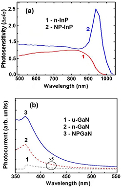
Figure 30. (a) Photosensitivity spectra of a bulk InP wafer (1), and a porous membrane (2) measured at room temperature. Reprinted from [52], Copyright (2010), with permission from Elsevier. (b) Photocurrent spectra measured from the undoped u-GaN (1), Si-doped n-GaN (2), and nanoporous NP-GaN (3) samples. The signal was normalized to the incident photon flux. Reprinted from [182], Copyright (2013), with permission from Elsevier.
Download figure:
Standard image High-resolution imageThe influence of the electrochemical etching upon the photosensitivity of porous materials is compared in table 8.
Table 8. The effect of electrochemical etching upon the photosensitivity of porous materials.
| Material | Ratio of the photosensitivity in porous to bulk material | Ref. |
|---|---|---|
| InP | 2.7 | [52] |
| GaP | 5 | [183] |
| GaAs | 6 | [181] |
| ZnTe | 1.3 | [82] |
The enhancement of photocurrent in nanoporous GaN (NP-GaN) made from Si-doped n-GaN as compared to the bulk n-GaN and undoped (u-GaN) is illustrated in figure 30(b) [182]. The photocurrent at the band gap wavelength (λ = 365 nm) in the NP GaN is larger by a factor of more than 60 as compared to the undoped GaN, and larger by a factor of more than 10 as compared to the n-GaN.
The enhancement of photocurrent has also been reported for a GaN photoelectrode obtained by photoelectrochemical etching in an environment-friendly etchant based on ionic liquids (figure 31(a)). The photocurrent of the porous electrode prepared by photoelectrochemical etching was two times higher as compared to the electrode produced by electrochemical etching, and six times higher as compared to the planar electrode [59].
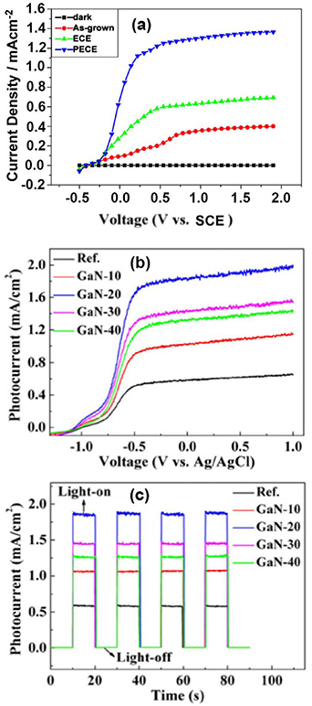
Figure 31. (a) Photocurrent response towards a series of potentials in 0.1 M HCl solution for a planar (as-grown) GaN electrode, and for porous electrodes fabricated by photoelectrochemical etching (PECE) and electrochemical etching (ECE). Reprinted from [59], Copyright (2016), with permission from Elsevier. (b) Photocurrent-voltage curves of the as-grown and GaN etched in 4.6 M HF aqueous solution during 10, 20, 30, and 40 min. (c) The photocurrent response. Reprinted from [41], Copyright (2018), with permission from Elsevier.
Download figure:
Standard image High-resolution imageIn good correlation with luminescence properties, which revealed a dependence of the photoluminescence intensity in porous GaN structures produced by photoelectrochemical etching in a 4.6 M HF aqueous solution upon the duration of the etching process (figure 29(a)), it was found that the photocurrent also increases by a factor of 3 with the increase of the etching time up to 20 min, while afterwards, it decreases with the etching time (figure 31(b)) [41]. The increase of the photocurrent in the porous sample etched during 20 min as compared to the as-grown one was explained by its larger surface-to-volume ratio, and the larger contact area between GaN and electrolyte, which results in a reduced aggregation of interfacial photogenerated carriers, thus avoiding the photocurrent crowding. The pore walls in the porous structure efficiently suppress the recombination of interfacial photogenerated carriers, while the increased charge separation efficiency leads to larger photocurrents in the etched GaN sample. The decrease of the photocurrent with the increase of the duration of the etching process above 20 min was explained by the increased optical reflectance and reduced optical absorption, due to changes in the porous morphology. Namely, the optical reflectance increases with the increase of the pore size, which was found to be larger in GaN-30 and GaN-40 samples. Figure 31(c) illustrates the photocurrent response.
Other phenomena enhanced by porosity are the long duration photoconductivity decay (LDPD) and persistent photoconductivity (PPC) [183, 184]. The investigation of the photocurrent built-up and decay in porous GaP and InP as a function of temperature and excitation light intensity suggested that these phenomena are determined by the porosity induced spatial potential barriers which hinder the recombination of photoexcited carriers. The pattern of the potential relief and the spatial potential barriers are controlled by the morphology and the porosity degree of the material which, in combinations with the presence of two components (fast and slow) in the PC decay, allows the elaboration of porous material based optoelectronic memory devices and switches [183].
All GaN samples (NP-GaN, n-GaN, and u-GaN) showed considerable PPC during the decay. However, it was concluded that the photoconduction was based on a different mechanism in the three types of materials [182]. Enhanced PPC with a longer relaxation time was observed in the NP-GaN as compared to n-GaN from which the nanoporous material was prepared. It was suggested that the PPC in NP-GaN is caused by surface states and by charge separation due to a strong electric field in the space charge region. This supposition was also confirmed by the increase of the yellow luminescence in NP-GaN, since previous investigations revealed a significant contribution of surface states to yellow luminescence. Band bending at the surface causes the formation of an energy barrier separating electrons and holes, and prohibiting the electron–hole recombination effectively, which results in a strong PPC effect. The higher activation barrier in nanoporous GaN resulted in a long lifetime of the photogenerated carriers, which was supposed to be beneficial for renewable energy devices such as solar cells and solar fuel devices. Therefore, the observed PPC in porous semiconductors is beneficial for the development of solar cells, optoelectronic memory devices and switches, but it could be detrimental for the development of photodetectors with fast photoresponse.
The problem of producing porous GaN with enhanced ultraviolet photoconductivity, but with reduced PPC, was solved by employing Pt-assisted electroless etching [185]. The photoresponse of porous GaN prepared from highly doped GaN (n > 1018 cm−3) showed a 15 times enhanced magnitude and faster decay of persistent photoconductivity as compared to the initial bulk crystalline GaN. The observed changes in photoconductivity have been explained in terms of a space charge model. It was suggested that the improved properties, i.e. enhanced photoresponse and faster PPC decay, make porous GaN a promising candidate for applications in UV photodetection and chemical sensing.
Similarly to the photoluminescence properties, the photoconductivity also depends on the chemical nature of the electrolyte used for electrochemical etching. Table 9 illustrates the enhancement of photoconductivity as a result of photoelectrochemical etching of various GaN materials in different electrolytes.
Table 9. The effect of photoelectrochemical etching of GaN in different electrolytes upon the photoconductivity enhancement.
| The GaN material | The electrolyte used | Ratio of the photo-conductivity in porous to bulk material | Ref. |
|---|---|---|---|
| HVPE-grown, Si-doped, electron conc. 4 × 1018 cm−3 | HF | 3.2 | [41] |
| Si-doped GaN, electron conc. 2.5 × 1018 cm−3 | Oxalic acid | 11 | [182] |
| HVPE-grown, Si-doped, electron conc. 4.8 × 1018 cm−3 | [BMIM]ClO4 ionic liquid | 3.5 | [59] |
| Si-doped GaN, electron conc. 1 × 1018 cm−3 | Pt assisted electroless etching in CH3OH-HF-H2O2 | 15 | [185] |
| MOCVD-grown undoped | KOH | 5.5 | [132] |
It can be seen from a comparison of data from tables 8 and 9 that higher photoconductivity enhancement is reached in porous GaN electrochemically etched in appropriate electrolytes as compared to other porous semiconductors.
The enhanced photoconductive properties of porous semiconductors are explored in the development of photodetectors, as described in section 5.
Apart from producing porous GaN materials, possibilities to fabricate arrays of GaN nanomembranes (15 nm thick) sustained by a network of pillars formed by GaN nanowires were demonstrated through the application of surface charge lithography (ion beam-writing of surface negative charge) followed by photoelectrochemical etching of MOCVD-grown GaN layers [186]. The fabricated arrays of nanomembranes exhibited memristive behavior due to the migration of the negatively-charged deep traps, which form in the volume of the membrane during the fabrication process, towards the unoccupied surface states of the suspended membranes. The time constant of the migration process was found to be of the order of tens of seconds and to vary with the current or voltage sweep. It was shown that single crystalline GaN nanomembranes arranged in simple networks consisting of parallel memristors are able to perform basic learning mechanisms such as habituation, dishabituation, and to memorize the learned responses to various electrical stimuli [187]. Such artificial learning mechanisms are analogous to non-associative learning processes which are identical in simple animals and human beings.
4.3. Optical phonon engineering by porosification
Introducing porosity in semiconductors is a versatile tool for a controlled modification of the phonon spectrum that is for phonon engineering. First of all, Froehlich type vibrational modes [188] are expected to occur in spontaneous Raman scattering from polar materials with the introduction of porosity, due to the enhancement of surface-to-volume ratio [189–193]. Different models have been applied for the theoretical explanation of the behavior of Froehlich modes in terms of the Maxwell-Garnett effective-medium expressions for the dielectric function based on the assumption that the structure can be described as built up from spheres [194]: the Bruggeman [195], the Sheng [196], and the Spanier-Herman models [197]. The properties of the Froehlich modes strongly depend on the morphology (i.e. symmetry, structural geometry, effective size, etc) and on the properties of the constituents of a composite material [198]. The vibration properties of porous materials are better interpreted using a 2D effective dielectric function [198, 199]. It was shown that the Froehlich modes are split into LO and TO components (FLO and FTO) in a porous medium, and their frequencies should be given by the maxima of Im[ eff(ω)] and Im[−1/eff(ω)], where eff(ω) is the dielectric function obtained from an effective medium expression which takes into account the degree of porosity (1 − c) and the morphology of the pores. C is the relative volume fraction of the semiconducting skeleton.
Figure 32(a) shows the mode frequencies for porous GaP as a function of the relative volume fraction c, calculated assuming pores filled with air [198]. The experimentally measured LO-FLO and LO-FTO splittings for three GaP porous samples are also indicated by dots in figure 32(a), and the Raman scattering spectrum measured at 10 K from a porous GaP sample with c = 0.55 is illustrated in figure 32(b) [200]. The good agreement between the experimental and calculated frequency values was considered to be a strong argument in favor of the Froehlich nature of the experimentally observed F1 and F2 modes. The temperature and pressure dependence of Raman scattering in porous gallium phosphide was investigated in details [200–202].
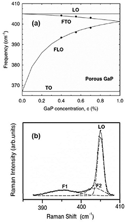
Figure 32. (a) Calculated frequencies of TO-phonon, LO-phonon and Froehlich modes as a function of the relative GaP concentration in porous GaP (dots refer to experimental data measured for three porous GaP samples with c-concentration of 0.40; 0.55; and 0.70). (b) Decomposition of the Raman spectra in the region of LO-phonon scattering at 10 K, from a porous GaP sample with c = 0.55. Reproduced from [200]. © IOP Publishing Ltd. All rights reserved.
Download figure:
Standard image High-resolution imageHowever, splitting of the Froehlich modes is observed in porous materials only at low temperatures, while usually only one Froehlich mode is observed at room temperature. On the other hand, other types of modes are observed at room temperature in both bulk and porous material, when the porous material is prepared on highly doped semiconductor, the so-called phonon–plasmon coupled (LOPC) modes. Two coupled modes L+ and L− arise in bulk materials. The L− is situated below the TO frequency, while the L+ mode is above the LO frequency, and these modes depend on the free-carrier concentration and on the carrier mobility. In addition to the L+ and L− coupled LOPC modes of the bulk material, coupled Froehlich–plasmon modes (F–T+, F–T−, F–L+ and F–L−) appear in the porous structures [198]. The L+ mode in the bulk material and the emergence of the Froehlich F mode are illustrated in figure 33(a) for a (111) GaP sample with free electron concentration of 2 × 1018 cm−3. According to the selection rules for a (111)-oriented surface, both the TO-phonon and LO-phonon modes are allowed in GaP. However, the inherent to undoped material pure LO-phonon is no longer observed in the doped bulk material due to the interaction of lattice vibrations with the free carrier plasma. Apart from that, the L– mode cannot be observed in GaP due to strong damping caused by the low mobility of the free carriers [192]. Note that both the L+ and L− modes are observed in highly doped GaAs, due to the high electron mobility inherent to this semiconductor. The LOPC mode of the doped bulk GaP substrate is no longer observed in the porous GaP sample. A strong peak of the LO-phonon is observed instead, along with the Froehlich F-mode. The occurrence of the unscreened LO-mode in the porous sample was interpreted in terms of the depleted from free carriers surface layer surrounding the pores, which is huge in the porous sample as compared to the bulk material [192].

Figure 33. (a) Raman spectra of (111) GaP measured at T = 300 K (F denotes the Froehlich mode, and L + is the LOPC mode). (b) Raman spectra of bulk and porous (100) GaAs measured at T = 77 K (L + and L– are the LOPC modes, while F-L + denotes the Froehlich-plasmon coupled mode. Reproduced from [198]. © IOP Publishing Ltd. All rights reserved.
Download figure:
Standard image High-resolution imageAs mentioned above, both the L+ and L− modes are observed in the bulk and porous GaAs, due to the high electron mobility as seen in figure 33(b). Diffuse scattering of the incident light inside the porous structures gives rise to the observation of strong TO-phonon mode, which is forbidden for the bulk material. The observation of the weak forbidden TO phonon in the bulk (100) sample is related to the crystal imperfection and/or to possible deviations from the true backscattering geometry. Additionally, Froehlich-plasmon coupled mode F-L+ is observed in the porous GaAs sample as discussed above.
In contrast to the bulk material, porous GaP layers were also shown to exhibit LOPC modes at low temperatures [202]. The occurrence of LOPC modes at low temperatures was explained taking into account that the porous GaP skeleton consists of both depleted surface layers surrounding the pores and conductive regions. The free electrons in these conductive regions were shown to be subjected to spatial confinement which increased with the decrease of temperature. The analysis of Raman scattering from the LOPC modes along with the data of electrical characterization and thermally stimulated conductivity indicated the formation of high conductivity regions embedded in a low conductivity porous GaP matrix at temperatures lower than 160 K.
Similarly to porous III–V semiconductors, the emergence of surface-related Froehlich modes was also observed in II–VI porous materials. Figure 34(a) illustrates the emergence of Froehlich modes in a porous ZnSe layer with cylindrical pores oriented perpendicularly to the sample surface, along with the TO, LO, and L+ modes observed in the bulk sample [203, 204]. The other bands observed in spectra represent two-phonon excitations as described elsewhere [205]. It was observed experimentally that the Froehlich mode is slightly shifted to lower frequencies for a longer wavelength. These observations were explained on the basis of the analysis of dispersion curves for surface-related modes, since their frequencies depend on the wavevector q measured along the cylindrical interface between a semiconductor with a dielectric function 2(ω) and a medium with a dielectric constant 1, i.e. their frequencies depend on cylinder radius r [204]. The calculated dispersion curves are shown in figure 34(b). The surface modes of the infinite planar surface are obtained in the limit of r → ∞.

Figure 34. (a) Raman spectrum of porous and bulk ZnSe samples measured at T = 300 K in the region of the optical phonons (the numbers correspond to two-phonon peaks). (b) Calculated dispersion of the Froehlich mode in ZnSe for cylindrical surfaces as a function of the radius r for different excitation wavelengths. Reproduced with permission from [204]. Reproduced from [204]. © IOP Publishing Ltd. All rights reserved.
Download figure:
Standard image High-resolution imageTherefore, porous semiconductors along with colloidal nanoparticles are unique materials from the point of view of the presence of Froehlich-type surface vibrational modes, which provide wide possibilities for phonon engineering. Note that surface vibrational modes have an impact on numerous physical quantities: adhesion, capillary force, crystal growth, the Casimir effect, etc [206].
Apart from exploring phonon engineering, Raman scattering is widely used to investigate the lattice integrity, and stress relaxation in porous semiconductors. Particularly, by using Raman scattering spectroscopy, it was shown that porous GaN obtained by photoelectrochemical etching (PECE) with ionic liquid as the etchant has better lattice integrity than that obtained by electrochemical etching (ECE) [59]. The data presented in figure 35 demonstrate that the Raman scattering spectrum of the PECE GaN is identical to the spectrum of the bulk as-grown sample. This observation indicates on the preservation of the lattice integrity in the PECE sample. At the same time, the spectrum of the ECE sample shows two additional peaks related to A1(TO) and E1(TO) phonons. It was suggested that the observed spectrum is indicative of the mixing of A1(LO) and E1(TO) modes, which occurs when the scattered radiation is not strictly parallel or perpendicular to the optical axis, i.e. the spectrum is indicative of the presence of lattice defects in the horizontal and vertical directions of the ECE sample.
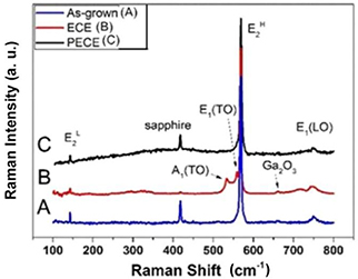
Figure 35. Raman spectra of as-grown planar and porous GaN prepared by ECE and PECE. Reprinted from [59], Copyright (2016), with permission from Elsevier.
Download figure:
Standard image High-resolution imageThe spectral position of the E2 (high) mode in GaN is used to estimate the relaxation of stress in porous layers as compared to the initial stressed bulk material. A relaxation of compressive stress of 0.13 GPa was estimated from the red shift of the E2 (high) mode in the porous GaN sample produced by PECE in a H2SO4:H2O2 electrolyte at 5 mA cm−2 current density [172]. It was shown that the relaxation of stress depends on the current density through the sample in the PECE process, as well as on the duration of the etching process. The stress was found to decrease by 0.25 GPa in the sample etched in a HF:C2H5OH electrolyte at the current density of 5 mA cm−2, while it is by 0.51 GPa for the sample etched at 20 mA cm−2 [169]. The compressive stress relaxation was shown to be improved by a longer duration of the etching process in a 4.6 M HF aqueous solution [41].
The relaxation of stress was also found to depend on the electrolyte composition used for porosification (table 10). The stress was relaxed by 0.25 GPa upon PECE in KOH and HF:HNO3 electrolytes, while it was by only 0.13 GPa upon PECE in HF:C2H5OH and H2SO4:H2O2 [171]. If this data is compared with those described above with reference to the influence of the electrolyte composition on the luminescence properties, it can be deduced that etching in a KOH electrolyte is beneficial for both the relaxation of stress and the enhancement of luminescence, while etching in the H2SO4:H2O2 leads to high luminescence intensity, but to a weaker relaxation of stress. In contrast, etching in the HF:HNO3 electrolyteresults in an effective relaxation of stress, but in a lower luminescence intensity.
Table 10. The relaxation of compressive stress in porous GaN layers deduced from the shift of the E2 (high) mode in Raman spectra.
| The GaN material | The electrolyte used | Shift of the E2 (high) peak (cm−1) | Stress relax. (GPa) | Ref. |
|---|---|---|---|---|
| HVPE-grown, Si-doped, electron conc. 4 × 1018 cm−3 | HF | 1.1 | 0.26 | [41] |
| Unintentionally doped n-GaN, electron conc. 2.3 × 1017 cm−3 | KOH | 2.1 | 0.50 | [166] |
| MOCVD-grown, Si-doped, electron conc. 4 × 1018 cm−3 | HF-ethanol | 2.1 | 0.50 | [169] |
| MBE-grown, electron conc. 2 × 1019 cm−3 | HF-ethanol | 1.7 | 0.41 | [170] |
| MOCVD-grown, Si-doped, electron conc. 1 × 1017 cm−3 | HF-ethanol HF-HNO3 KOH H2SO4-H2O2 | 0.53 1.06 1.06 0.53 | 0.13 0.25 0.25 0.13 | [171] |
| MOCVD-grown, Si-doped, electron conc. 5 × 1018 cm−3 | HF Porous layer on the substrate Detached porous membrane | 0.6 3.0 | 0.14 0.71 | [207] |
It can be seen from table 10 that a significant relaxation of stress occurs in GaN layers deposited on substrates as a result of electrochemical porosification in various electrolytes, as deduced from the redshift of the E2 (high) Raman mode, using the calibration constant of 4.2 cm−1 GPa−1. A total relaxation of stress, which amounts 0.71 GPa, was measured in a porous GaN membrane detached from the substrate [207]. The position of the E2 (high) Raman peak in the porous membranes perfectly corresponds to the respective position in the bulk unstressed GaN material.
Apart from GaN materials with different porosities, the relaxation of compressive stress via introducing porosity was demonstrated by Raman scattering investigations in more complex multiple quantum well (MQW) structures based on GaN-related materials subjected to UV-assisted EC etching [56]. The relaxation of stress was shown to result in enhanced light emission from GaN-based LEDs thin films with InGaN/GaN MQWs, due to improved internal quantum efficiency.
4.4. Enhanced nonlinear optical properties: second harmonic generation and terahertz emission
In addition to improving linear optical, luminescence and photoelectrical properties, making semiconductor material nanoporous by EC and PEC etching is a powerful tool for enhancing their nonlinear optical properties. Porous materials are actually composite materials constituted from two components: semiconducting skeleton and pores filled with air. It was found in an early study that the effective third-order susceptibility of a composite optical material formed of sub-wavelength-thick layers of titanium dioxide and a conjugated polymer can substantially exceed those of the materials from which it is constructed [208]. Among porous materials, enhancement of nonlinear optical properties was first demonstrated in GaP [209–211] and InP [212, 213]. It was demonstrated that both second harmonic generation (SHG) and terahertz (THZ) emission are increased in porous materials as compared to their bulk counterparts. Several things are important for second harmonic generation: (i) porous sample optical homogeneity to avoid strong light scattering; (ii) high value of the second order nonlinear optical coefficient; (iii) large third order electric field fluctuations; and (iv) birefringence to ensure phase matching.
Figure 36 compares the rotational dependence of the second harmonic intensity for a porous optically homogeneous GaP membrane and for an inhomogeneous one. The rotational dependence for an optically homogeneous porous GaP (111) membrane possessing triangular-prism-like pores reflects perfectly the crystallographic features of (111)-oriented GaP demonstrating the high crystalline quality of the porous skeleton. The relatively small dimensions of both pores and the skeleton entities (50 ÷ 100 nm) as compared to the wavelength of the electromagnetic radiation (1064 nm) make the porous medium optically homogeneous in spite of a statistical distribution of pores. On the contrary, the optically inhomogeneous GaP membrane reflects no crystallographic features as a consequence of strong diffuse scattering.
Figure 36. SH intensity induced by a 1064 nm polarized pump beam at normal incidence as a function of the azimuthal rotation angle of the optically homogeneous (solid squares) and inhomogeneous (solid triangles) porous GaP membranes measured in parallel polarization. The solid line is a fit. [211] John Wiley & Sons. Copyright © 2003 WILEY-VCH Verlag GmbH & Co. KGaA, Weinheim.
Download figure:
Standard image High-resolution imageAs concerns the nonlinear coefficients, it is known that they are large for III–V compounds. For instance, bulk GaAs possesses a second order nonlinear optical coefficient which is several orders of magnitude higher than that of KDP, ADP and other materials used in upconversion [214].
As concerns the electric field fluctuations, it was shown that noncylindrical pores (i.e. triangular prism-like pores in the GaP (111) membrane) can result in large third order fluctuations which strongly intensify the nonlinear optical response [209, 211]. Figure 37(a) demonstrates that, under identical conditions, the porous GaP membranes with triangular prism-like pores exhibit a SHG efficiency two orders of magnitude higher than that of the bulk material [210]. In spite of the electric field screening in the semiconductor, the third order field fluctuations responsible for the SHG are very large in case of pores with sharp edges. It was also suggested that, taking into account existing theories, an important role in the SHG enhancement may be attributed to the material percolation which is also responsible for the mechanical stability and good thermal conductivity of porous membranes.
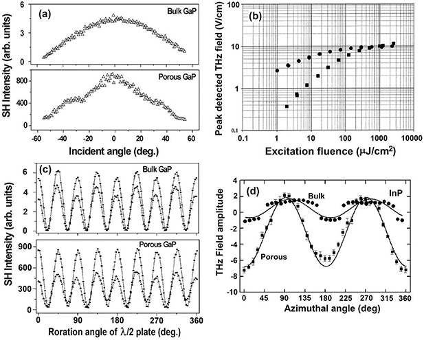
Figure 37. (a) Measured s-polarized SH intensity as a function of the incident angle of the s-polarized fundamental beam for bulk (111)-oriented GaP and porous GaP. Reproduced with permission from [210]. (b) Peak detected THz field as a function of pump fluence for porous (filled circles) and bulk (filled squares) InP (111) samples. Reprinted from [213], with the permission of AIP Publishing. (c) Measured s-polarized SH intensity as a function of the rotation angle of the half-wave plate for bulk and porous GaP at two angles of incidence of the pump beam: normal incidence porous (squares) and 30° (triangles). [210] John Wiley & Sons. © 2000 WILEY-VCH Verlag Berlin GmbH, Fed. Rep. of Germany. (d) Azimuthal dependence of the p-polarized THz field amplitude in reflection from the porous (squares) and bulk (circles) InP (100) samples under p-polarized excitation. Reprinted with permission from [212], Copyright (2005) by the American Physical Society.
Download figure:
Standard image High-resolution imageFigure 37(c) shows the fundamental polarization dependence of the s-polarized SH intensities for bulk and porous GaP at two different angles of incidence of the pump beam. It can be noticed that the porous membrane exhibits as strong nonlinear optical anisotropy as the bulk GaP, and no isotropic contribution induced by the multiple scattering of light in the porous network is observed, which demonstrates again the optical homogeneity of the membrane. The analysis of these data suggested that the studied membranes fulfil the phase matching conditions, provided that the fundamental and SH beams propagate in directions that are nearly perpendicular to the pores [210]. It was shown that the phase matching angle is a function of the GaP concentration in the porous medium [211].
Similarly to second harmonic generation, introducing porosity is also expected to enhance the related phenomenon of optical rectification (OR), which should in turn lead to the enhanced emission of pulsed THz radiation from porous surfaces. A significant enhancement of THz emission was demonstrated from porous InP surfaces under the excitation with 120 fs pulses of 800 nm radiation from a Ti:Sapphire amplified laser system [212, 213]. Figure 37(b) shows that the peak THz field saturates at a high excitation fluence from both bulk and porous InP, however, the emission from the porous InP (111) membrane is approximately 10 times as large as that from the bulk InP at lower excitation fluences (2 µJ cm−2). It should be noted that an order of magnitude increased radiated field amounts to a relative power increase of approximately two orders of magnitude.
As concerns the mechanisms of THz emission from semiconductor surfaces, there are contributions from several mechanisms, including photocarrier effects and nonlinear optical processes. Particularly, it was shown for InP that photocarrier acceleration in the surface depletion field dominates at room temperatures and low-excitation fluence, whereas bulk OR and photocarrier diffusion dominate at higher fluences, with the crossover in mechanisms occurring at fluences between 0.1–10 mJ cm−2 [213]. Investigation of the azimuthal dependence of the s-polarized and p-polarized THz field amplitude in reflection from the porous (squares) and bulk (circles) InP (100) samples under p-polarized excitation was carried out to estimate which process is being enhanced (figure 37(d)). It was found that the azimuthal dependence of the THz field in the p-p geometry is well fitted to the form of ETHz = a cos(2φ) + b, i.e. there is an angularly independent contribution to the radiated THz field, which is indicative of some photocarrier effects. However, investigations in the p-s geometry revealed that the s-polarized THz field is nonzero, and has the expected twofold rotational symmetry associated with a second-order nonlinear response from (100)-oriented InP. Apart from that, the angularly independent contribution to the s-polarized THz field is less than 10%. These results indicate that the s-polarized THz emission is primarily due to optical rectification.
Therefore, porosity-based technological approaches prove to be very important for elaborating new nonlinear optical elements ready to be integrated in optoelectronic circuits. The formation of pores leads to symmetry breaking and to the porosity-induced artificial birefringence. In particular, pores parallel to the <111> direction in III–V compounds change the cubic crystal symmetry (point group Td) to the uniaxial trigonal one (point group C3v). The investigation of porosity-induced birefringence in GaP membranes using a method based on the analysis of beats in transmittance spectra and angular dependence of optical spectra revealed a birefringence as high as (ne − no) = 0.25 in a porous GaP membrane with the degree of porosity close to 40% [214]. As mentioned above, the porosity-induced artificial birefringence opens the possibility to meet the phase matching conditions for the second harmonic generation in III–V materials. The lack of birefringence in bulk III–V semiconductors with cubic structure is a fundamental obstacle in making use of their advantageous second order optical coefficients, as seen in table 11.
Table 11. Second-order optical coefficients of nonlinear-optical materials.
| Material | Birefringence,
| Coefficient | Value at 1.064 µm (pm V−1) | Ref. |
|---|---|---|---|---|
| Quartz | 0.009 | d11 | 0.30 | [215] |
| KDP | 0.034 | d36 | 0.39 | [215] |
| ADP | 0.039 | d36 | 0.47 | [215] |
| KTP | 0.092 | d33 d31 | 14.6 3.7 | [215] |
| LiNbO3 | 0.076 | d33 d31 | 25.2 4.4 | [215] |
| KNbO3 | 0.14 | d33 d31 | 19.6 10.8 | [215] |
| LiIO3 | 0.14 | d31 | 4.2 | [216] |
| AgGaS2 | 0.053 | d36 | 22 | [217] |
| Bulk GaP | No birefringence | d36 | 70.6 | [215] |
| Por. GaP | 0.25 (at 40% porosity) | SHG efficiency | ~100 increase as compared to the bulk | [209, 214] |
| Bulk InP | No birefringence | dSHG | 300 (at 10.6 µm) | [218] |
| Por. InP | Adjusted by porosity | SHG efficiency | ~ 30 increase as compared to the bulk | [212] |
| Bulk GaAs | No birefringence | d36 | 170 | [215] |
| Por. GaAs | Adjusted by porosity | SHG efficiency | not explored |
The analysis of data in table 11 clearly demonstrates the prospects of porous III–V materials for nonlinear-optical applications.
Apart from that, new nonlinear optical media can be created just by filling in the pores in porous III–V compounds with other materials. In this case, the semiconductor skeleton can be designed to provide phase matching while the material filling the pores will contribute mainly to the SHG. It was suggested that porous III–V compounds as phase-matching matrices are much more promising than elementary semiconductors due to their larger band gap and their more pronounced anisotropy when subjected to electrochemical etching [211].
The observation of increased THz emission from porous samples is also of importance to the THz community as application areas for pulsed THz radiation grow. In particular, emitters with improved efficiency are needed for THz imaging [212].
5. Applications of porous semiconductor compounds
5.1. Surface enhanced Raman scattering
In addition to exploring phonon engineering and using Raman scattering for estimating the quality and stress in the prepared porous materials, porous matrices represent a versatile platform for developing surface enhanced Raman scattering substrates. Actually, the porous semiconductor matrices, in conjunction with metallic nanoparticles deposits, represent a component of metal-dielectric nanostructured materials which are regarded as a class of nanocomposites with great application potential in photonics and optoelectronics. Metal nanostructures can exhibit strong local resonances of light-induced electron plasma oscillations. Due to such resonances, irradiated light is absorbed rather than reflected and the electromagnetic field intensity close to the surface of the nanostructures can be strongly enhanced. These electromagnetic fields lead to fascinating enhancement of optical characteristics, the surface-enhanced resonant Raman scattering (SERS) being among them [219]. Over the last few decades, SERS spectroscopy has demonstrated its power as an ultra-sensitive and non-destructive analytical tool in various fields, including electrochemistry, environmental analysis and biochemical science.
The electromagnetic enhancement mechanism of SERS involves an enhanced electric field present at a noble metal surface that couples to and enhances the efficiency of the Raman modes of nearby molecules. This field is caused by locally confined surface plasmons in the metal, meaning that for a noble metal surface to be SERS-active, it must have nanoscale features to create the large local optical fields required.
The efficacy of SERS substrates is typically assessed by their enhancement factor (EF), which is the increase in the Raman signal in the SERS experiment over an unenhanced experiment. Values of the EF range from 104 to 1014 depending on the substrate used, a value of 106–108 being considered typical.
Among porous semiconductors, GaN is the most frequently used material for the preparation of SERS substrates, and Au and Ag deposits are preferential metal inclusions. Porous GaN (PGaN) templates are prepared by various technological procedures as described in the previous sections of this work. Metal-assisted PEC etching and metal-assisted electroless etching technique ensures obtaining of a wide variety of 2D and 3D morphologies suitable for the preparation of SERS substrates. High values of the EF were demonstrated with SERS substrates prepared by depositing Au or Ag on PGaN templates generated by a Pt-assisted electroless etching technique [220]. The Au or Ag inclusions were deposited by a solution-based electroless deposition, as shown in figure 38(a). As can be seen in the SEM images, the morphology of the deposited Au is dominated by spheroidal Au structures that rest on the surface and are attached in the pores. The SEM investigation performed in cross-section demonstrated the deposition of Au nanoparticles to a significant depth (>1 µm) below the outer surface. The SERS spectrum of MGITC recorded with the excitation wavelength of 752.5 nm in such a substrate with Au as metal is shown in figure 38(b). It was found that the highest overall SERS response, with an enhancement factor relative to normal Raman spectroscopy of 108, was obtained with Ag deposition. It was suggested that the increase in EF relative to typical SERS-active substrates is assigned partly to the large surface area inherent to the PGaN-Ag structures, and partly to the specific morphology of the metal-nanopore composite structure.

Figure 38. (a) Plan-view SEM image of a PGaN substrate with an electrolessly deposited Au film. (b) SERS spectrum of MGITC. Reprinted with permission from [220]. Copyright (2005) American Chemical Society. (c) SEM image of the AgNPs/GaN NF substrate. (d) SERS spectra of 10–6 M R6G adsorbed on different AgNPs/GaN substrates. Reprinted from [221], Copyright (2017), with permission from Elsevier. (e) SEM images of photo-etched GaN bunches of nanopillars covered by as-sputtered Au-Cu alloy. (f) SERS spectra of 4-MBA recorded on the same platform covered by Au-Cu alloy with/without large pits/nanopilars. Reprinted with permission from [222]. Copyright (2016) American Chemical Society. The spectra shown in (b), (d), and (f) were measured on substrates imaged in (a), (c), and (e), respectively.
Download figure:
Standard image High-resolution imageA similar enhancement was demonstrated for the Rhodamine 6 G (R6 G) with 3D metal-semiconductor nanostructures designed by in situ electrodeposition of AuNPs, or in situ photodeposition of AgNPs on gallium nitride nanoflowers (NF) supports fabricate by metal-assisted PEC etching of single crystalline GaN [221] (figures 38(c) and (d)). It was found that metal NPs/GaN NFs substrates ensures higher EF as compared to GaN NFs without metal nanoparticles as well as compared to metal NPs deposited on planar GaN and porous GaN templates. EF of SERS for AuNPs/GaN NFs and AgNPs/GaN NFs were 2 × 10⁷, and 6 × 10⁷, while the corresponding detection limits of R6G were 10–8 and 10–10 M, respectively. It was suggested that 3D substrates are more suitable for SERS compared to 2D substrates, since 3D substrates have more 'hot spots' which can generate greater enhancement, and 3D substrates can provide a larger surface area, which can interact with more target molecules. The performance of such substrates for biological applications was also demonstrated by the detection of bovine serum albumin (BSA), which indicates their good biocompatibility and prospects for SERS biosensors.
Even lower detection limits, as low as ~1016 M of R6G, approaching single-molecule detection, was demonstrated with ultrasensitive SERS substrates fabricated by electrodepositing Au nanoparticles with the average sizes of ~20 nm onto porous GaN. Such a performance was attributed to the preferable sizes of Au NPs with high plasmonic activity, lots of nano-gaps between Au NPs, and perfect synergistic effect with porous structure [223].
Apart from Au and Ag metals, it was shown that SERS can be realized with Au-Cu thin film deposited on photo-etched (nanostructured) templates in the form of GaN bunches of nanopillars [222] (figure 38(e)). Such substrates have been tested using pyridine and 4-mercaptobenzoic acid (4-MBA) (figure 38(f)). A comparative study of depositing Au-Cu thin films on three types of GaN templates (templates with nanopillars, templates with large etched pits, and templates with both etched pits and nanopillars) was performed, which revealed that the best SERS substrates are those with both etched pits and nanopillars (figure 38(f)). The EF for the three types of substrates was found to be 1 × 10⁵, 3 × 10⁵, and 5 × 10⁵, respectively. The effect of dealloying after the Au-Cu thin film deposition was investigated with the purpose of producing stable SERS-active platforms. It was demonstrated that dealloying of deposited Au-Cu films, which results in the increase of the nanoporosity of the Au-Cu films and the decrease of the Cu percentage at the surface of the alloyed layer, gives very stable SERS substrates.
Table 12 compares the data for SERS with various substrates.
Table 12. SERS EF and detection limit for substrates with different material systems.
| Material system | Enhancement factor (EF) | Detection limit | Ref. |
|---|---|---|---|
| The typical value of the EF taken as reference | 106 | — | [224] |
| GaN bunches of nanopillars covered with Au-Cu thin film | 5 × 10⁵ | — | [222] |
| AgNP/PGaN | 108 | — | [220] |
| AgNPs/GaN NF | 6 × 10⁷ | 10–10 M for R6G | [221] |
| AuNPs/GaN NF | 2 × 10⁷ | 10–8 M for R6G | [221] |
| AuNP/PGaN | 108 | 10–16 M for R6G | [223] |
The analysis of data in table 12 shows that the EF for substrates covered with Au-Cu thin film is lower than the typical value of 106. However, it should be taken into consideration that the cost of such substrates is lower than those using pure Au or Ag films. The other substrates demonstrate EF up to 108.
5.2. Energy storage
Nanostructures made their debut in photovoltaics in 1991 with the invention of dye sensitized solar cells (DSSC) by Michael Grätzel [225]. This incorporates a layer of nanoporous TiO2 (formed by high temperature sintering of nanoparticles) that is sensitized with a Ruthenium dye and contacted by an iodide containing electrolyte. However, the high temperature sintering step in the case of TiO2 nanostructures brings disadvantages from several points of view, such as increased costs, difficulties with using flexible plastic substrates, etc. Electrochemical nanostructuring of semiconductor substrates as well as electrochemical deposition of nanoporous films represent low-temperature technological approaches.
Another advantage of porous structures produced by electrochemical etching, similarly to ZnO nanorod structures produced by electrochemical deposition, as compared to mesoporous nanoparticulate films, relies on larger voids inherent to their morphology. These peculiarities provide better conditions for filling these voids with solid hole-transporting material (HTM), which is important in developing solid-state DSSC. For solid-state DSSCs, to effectively fill thick nanoparticle-based mesoporous TiO2 films with HTMs remains challenging [226].
Solar-to-electrical energy conversion efficiency of the DSSC with electrodeposited ZnO electrode, liquid electrolyte and D149 dye amounts to 5.6% [227]. Similar efficiency of 5.65% was achieved in a solid-state DSSC based on TiO2 coated ZnO nanowire arrays with spiro-OMeTAD as the solid-state HTM [226].
The photoetching of semiconductor substrates affects the photovoltaic performance of semiconductors by increasing the collection efficiency of photogenerated carriers, which results in improved photocurrents [228]. It was shown that photoetching of CdS (CdSe) surfaces produces a porous fractal-type morphology with superior photovoltaic properties [163]. The photoelectrochemical etching was found to improve the output characteristics of CdSe-polysulfide photoelectrochemical cells with both single-crystal and polycrystalline CdSe [229]. An increase in shortcircuit current (SCC) was observed for single-crystal CdSe, while both the SCC and the fill factor were improved in polycrystalline CdSe. The improvement was explained by the decreased reflectivity of the surface and by the removal of near-surface recombination centers during the photoelectrochemical etching.
Figure 39 illustrates the scheme of the charge separation process at the donor:acceptor interface of a DSSC based on the electrochemically nanostructured CdS surface. At step (1), light produces excitons by the photoexcitation of dye (D∗); at step (2), the excitons will migrate to the CdS/dye interface, dissociate, and inject electrons into the conduction band of the CdS semiconductor, leaving holes (D+) in the dye; at step (3), the dye is regenerated by accepting electrons from the reduced state of the redox couple (RE), producing the oxidized state of the redox couple (OX) in the electrolyte; at step (4), the electrolyte is regenerated via OX accepting electrons from the counter electrode and producing RE; at step (5) the injecting electrons will recombine by donating electrons to D+; and at step (6), the injected electrons recombine by donating electrons to OX. Therefore, the full cycle is closed. In order to obtain an efficient DSSC device, it is very important to have a fast injection process of electrons from the excited dye molecules to the conduction band of the CdS, and a fast translation from the conduction band of CdS to the FTO electrode.
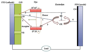
Figure 39. (a) Structure and operating principle of CdS/dye-sensitized solar cells: (1) photoexcitation; (2) electron excitation; (3) dye regeneration; (4) electrolyte regeneration; (5) recombination by D+; (6) recombination by OX. Reprinted from [221], Copyright (2017), with permission from Elsevier.
Download figure:
Standard image High-resolution imageThe use of solid solutions provides even more possibilities for improving the DSSC efficiency, due to possibilities to model the scheme of the charge separation process. Photoelectrochemical solar cells (PECs) with solar-to-electrical conversion efficiency of up to 8% were demonstrated on CdSe0.65Te0.35 electrodes [230].
Table 13 compares the data for several DSSCs prepared on PEC etched CdSeTe solid solutions and electrochemically deposited ZnO structures.
Table 13. Comparison of DSSC prepared on PEC etched CdSeTe solid solutions and electrochemically deposited ZnO structures.
| Type of solar cell | Electrolyte used | Solar-to-electrical conversion efficiency | Ref. |
|---|---|---|---|
| DSSC with nanocrystalline TiO2 film electrode | Liquid electrolyte | 12,3 | [232] |
| DSSC with electrodeposited ZnO electrode | Liquid electrolyte | 5.6% | [227] |
| DSSC based on TiO2 coated ZnO nanowire arrays | Spiro-OMeTAD as the solid-state HTM | 5.65% | [226] |
| DSSC with sintered nanoparticle-based mesoporous TiO2 photoelectrode | Spiro-MeOTAD as the solid-state HTM | 7.2% | [233] |
| PECs with photoetched CdSe0.65Te0.35 photoelectrode | Polysulphide | 8% | [230] |
It can be seen from table 13 that solar cell efficiencies higher than 12% can be obtained with DSSC based on nanocrystalline TiO2 electrode and liquid electrolyte. However, this type of material is not well suitable for all-solid-state DSSC. The maximum efficiencies reached with solid-state DSSC do not exceed 8%. Similar efficiencies were obtained with PECs based on photoetched ternary CdSTe compounds. Taking into account that the design of such solar cells was not optimized both in terms of solid solution composition and photoetching parameters, it can be expected that higher solar cell efficiencies are feasible.
Photoelectrochemical solar cells were also tested with a porous GaAs photoelectrode, a carbon auxiliary electrode and colloidal aqueous solution of Na2SiO3 [181]. The study showed that introduction of porosity in the photoelectrode leads to the increase of the photosensitivity in the long-wavelength region near the band gap of GaAs, and leads to the increase of the short-circuit current by a factor of two, which corresponds to the output power increase by a factor of four.
A recent study demonstrated that porous GaN crystal membranes are good potential electrode materials for energy storage devices [39]. The cell based on these membranes manifested ultrahigh power density (45 mW cm−2), and the fabricated supercapacitors manifested excellent electrochemical characterization (99% capacitance retention after 10 000 cycles). A specific capacitance of more than 23 mF cm−2 at the current density of 0.5 mA cm−2 has been demonstrated with single crystal gallium nitride mesoporous membrane prepared through an electrochemical etching process [234].
Table 14 compares the data for supercapacitors prepared on various materials.
Table 14. Parameters of supercapacitors prepared on various materials.
| Type of material | Power density | Specific capacitance | Cycle stability | Ref. |
|---|---|---|---|---|
| Porous GaN crystal membranes | 45 mW cm−2 at current density of 10 mA cm−2 | 21 mF cm−2 at current density of 0.1 mA cm−2 | 99% capacitance retention after 104 cycles | [39] |
| GaN mesoporous membrane | 38 mW cm−2 at 10 mA cm−2 | 23 mF cm−2 at 0.5 mA cm−2 | 96% after 5 × 10⁴ cycles | [234] |
| Si nanowires grown in 3 µm alumina templates | 16 mW cm−2 at 0.5 mA cm2 | 16.5 mF cm−2 at 0.5 mA cm2 | 99% after 3 × 10⁵ cycles | [235] |
| Si nanowires coated with TiO2 | — | 3.5 mF cm−2 at 0.1 mA cm−2 | 75.7% after 103 cycles | [236] |
| Hierarchical mushroom-like CoNi2S4 arrays | — | 5.7 mF cm−2 at 20 mA cm−2 | 81% after 103 cycles | [237] |
| Nitrogen Doped SiC nanowires | 72 mW cm−2 at 30 mA/cm2 | 4.8 mF cm−2 at 30 mA cm−2 | 98% after 104 cycles | [238] |
| Hydrogenated TiO2 Nanotubes | 17.5 mW/cm2 | 3.3 mF cm−2 at 0.02 mA cm−2 | 97% after 104 cycles | [239] |
The analysis of data in table 14 shows that the supercapacitors based on porous GaN membranes demonstrate better energy storage capacities in terms of power density and specific capacitance at lower current density, as compared to other materials. For instance, the parameters of supercapacitors based on Si nanowires grown in alumina templates are better than those of the devices based on Si nanowires prepared by metal-assisted chemical etching and coated with TiO2. At the same time, the parameters of the devices developed on porous GaN membranes are better as compared to those of supercapacitors based on Si nanowires grown in alumina templates.
Nanoporous GaN materials are regarded as very promising nanostructures for solar powered hydrogen generation, as they provides a number of advantages due to enhanced surface-to-volume ratio and reduced carrier travelling distance, which ensures the participation of energetic electrons/holes in both the oxygen-evolution half-reaction and the hydrogen-evolution half-reaction before their recombination. Two types of GaN based photoelectrodes with either horizontally aligned or vertically aligned nanopores have been fabricated by means of electrochemical etching [240]. Detailed solar powered hydrogen generation experiments including applied bias photon-to-current efficiency (ABPE) and incident photon-to-current efficiency (IPCE) demonstrated a significant enhancement in photocurrent density compared to their planar counterpart. The prepared photoelectrodes demonstrated an up to 5-fold enhancement in ABPE and IPCE in comparison with their planar counterpart. Stable hydrogen generation was observed at a zero bias potential versus the counter-electrode with GaN nanomaterials [241].
5.3. Photocatalytic applications, water splitting
Apart from hydrogen production via water splitting, photocatalysis is widely used in environmental remediation. Porous material offer many advantages for these applications due to their enhanced photocatalytic properties related to their increased surface-to-volume ratio. As a consequence of the increased surface-to-volume ratio, the reaction areas as well as the light absorption are largely increased and the charge carriers are effectively separated. After porosification, the migration distance of photogenerated carriers toward the semiconductor/solution interface is reduced, the recombination of the photogenerated carriers is suppressed, and the photocurrent is significantly increased.
The mechanisms of the photocatalytic activity depend on the composition of the porous photoelectrode or composite material prepared on the basis of porous structures, as well as on the bandgap energetic alignment with the redox potentials. Figure 40 schematically illustrates the mechanism for photocatalytic process with several porous and composite materials. For a nanoporous GaN photoelectrode, the process of photodegradation of dyes can be roughly divided into four stages [242] (figure 40(a)). At stage (I), photoexcitation in the nanopores occurs, at which electron-hole pairs are created by UV light illumination, provided the photon energy is greater than the GaN bandgap energy. At this stage, the catalyst is transformed into the photoexcited state. At stage (II), the electron-hole pairs are separated and subsequently transferred to their sites on the interface of GaN nanopores. In parallel with stage (II), stage (III) occurs, at which a fraction of photogenerated electrons and holes radiatively or nonradiatively recombine, or are trapped by the defects on the internal surface of GaN nanopores. At stage (IV), the redox reaction occurs, at which the adsorbed water and the dissolved oxygen are involved to ·OH radicals which are strong and nonselective oxidizing agents for organic pollutants. Finally, the dye molecules are oxidized and decomposed by the ·OH radicals.
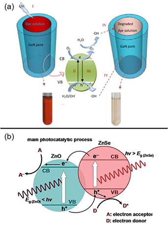
Figure 40. (a) Schematic illustrating the mechanism for photocatalytic process in GaN nanopores: (I) photoexcitation in the nanopores, (II) charge separation and transportation, (III) charge recombination in parallel to stage II, and (IV) photoassisted redox reaction. Reprinted from [242], Copyright (2015), with permission from Elsevier. (b) Energy band structures of a region of the ZnO/ZnSe nanocomposite and the main photocatalytic process of the Orange-II decomposition. Reproduced from [243] with permission of The Royal Society of Chemistry.
Download figure:
Standard image High-resolution imageFigure 40(b) illustrates how the main photocatalytic process of dye decomposition is governed by the energy band structures of a porous ZnO/ZnSe nanocomposite [243]. The main photocatalytic processes of the synthesized nanostructures were driven by photo-excitation of the semiconductor (ZnO or ZnSe) under the absorption of light with the quantum energy equal to or exceeding the band gap energy. The formation of a diffusion potential is induced by the staggered valence and conduction bands of ZnSe component of the composite material with respect to those of the ZnO component. This diffusion potential is an electromotive force for the electron injection, which transfers the electrons to the conduction band of ZnO, while the holes remained in the ZnSe valence band. Therefore, charge separation of the electron–hole pair occurs before recombination. As a result of separation, holes in ZnSe directly oxidized dye molecules adhering to the surfaces of ZnSe nanoparticles. The exposed ZnO crystalline phase was also suggested to play a role in dye degradation by means of the reaction of electrons at the ZnO surface with oxygen, which could accept electrons to form a superoxide radical anion (O2 ·). The formed superoxide radical anions were suggested to further form hydroxyl radicals, which degraded the dye molecules [243]. It was shown that the porous ZnO–ZnSe nanocomposites have much higher visible light photocatalytic activities than the porous ZnO or the ZnSe nanostructures, and it was suggested that such composite materials may find use as solar energy conversion materials.
It was shown that the nanoporous GaN exhibited much better photocatalytic activity for the degradation of the 4BS dye as compared to both the plane GaN thin films and the porous Si wafers, because GaN is efficient not only for dye reduction, but also for dye oxidation (see table 15). It was also found that the nanoporous GaN has excellent stability to photodegrade organic dye as compared to porous Si under basic conditions. Taking into account that the bandgap of GaN can be tuned in the visible-light region by alloying with InN, it was suggested that the nanoporous GaN is a prospective material for photodegradation systems with concentrated solar light.
Table 15. Comparison of organic dye photodegradation properties of porous GaN and porous Si.
| Material | Dye oxidation/dye reduction | Change in the surface morphology after dye photodegradation | Photodegradation of the cromophoric structure of the organic dye |
|---|---|---|---|
| Porous Si | No/yes | Yes | 33% |
| Porous GaN | Yes/yes | No | 57% |
Porous GaN structures prepared by a lateral anodic etching process in HNO3 solution in combination with a laser scribing (LS) process to expose the side walls of n-GaN film demonstrated much better water splitting properties as compared to the as-grown GaN film [130]. The laterally porous photoanode nearly showed a 3.4 times enhancement of self-driven photocurrent compared with the as-grown GaN film. An even higher increase of the saturation photocurrent during the water splitting by a factor of ~4.5 was achieved with a composite porous GaN structure with both well-ordered lateral and vertical holes designed and fabricated based on the laterally porous GaN [244]. Investigation of the mechanism for the enhancement of the water splitting performance using the FDTD method revealed that the well-ordered vertical holes play a double role in opening the embedded pore channels to electrolyte at both sides, which reduces the migration distance of the gas bubbles during the water splitting reactions, and in modulating the light field, which results in trapping most of the incident light into the nanoholes. Thus, the electric fields localized in the lateral pores can increase dramatically as a result of the strong optical coupling. These results demonstrate large prospects of implementing porous GaN photoelectrodes for the high-efficient solar water splitting.
5.4. Photodetectors, sensors for environmental monitoring
The enhancement of photoconductivity by porosity described in the previous section indicates on the applicability of porous semiconductors in the development of photodetectors, while the enhanced photocatalytic properties are in relations with their suitability for the development of chemical sensors. Photodetectors have been reported on the basis of several porous semiconductors and composite materials. Figure 41 demonstrates prototype devices elaborated on the basis of bulk and porous GaN in conjunction with a poly(3-hexilthiophene) P3HT polymer [245]. Both types of devices exhibit obvious rectifying characteristics and photosensitivity. However, the rectification ratio at the applied bias of 2 V was found to be higher by a factor of 27 for the device fabricated with porous GaN in the dark, and higher by a factor of 54 under the UV illumination, as compared to the device fabricated with bulk GaN. The photosensitive properties of the device with porous GaN were also better as compared to the device with bulk GaN: the Ion/Ioff ratio of 6.7 against 1.7.
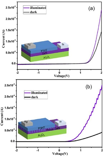
Figure 41. I–V characteristics of prototype devices in dark and under illumination: (a) Ag/P3HT/GaN/In; (b) Ag/P3HT/PGaN/In. PGaN was prepared after etching for 15 min. The insets are corresponding device configurations. Reprinted from [245], Copyright (2014), with permission from Elsevier.
Download figure:
Standard image High-resolution imageHigh-detectivity ultraviolet metal-semiconductor-metal (MSM) photodetectors with a value of the specific detectivity up to 5.3 × 10¹⁴ Jones under UV illumination have been demonstrated on the basis of laterally mesoporous GaN [246]. The high specific detectivity was attributed to the trapping of photo-generated holes at the mesoporous GaN/metal contact interface, which lowers the Schottky barrier height, thus causing a large internal gain. The photodetector was demonstrated to be very sensitive to photons with wavelength λ < 350 nm. The selective detection of the photodetector to UV light was demonstrated by the large UV/visible rejection ratio, which is defined as the ratio between the photoresponse at λ = 350 nm and λ = 400 nm, and was found to be ~100 and ~400 at V = 1 V and V = 0.5 V, respectively. Note that the photodetectors based on non-mesoporous GaN, fabricated as reference samples, showed practically no measurable photo-response.
Figure 42(a) shows the photocurrent and the specific detectivity D* of a photodetector based on mesoporous GaN for incident UV (λ = 340 nm) light of power P. The value of D* decreases with increasing power, a maximum specific detectivity D* = 5.3 × 10¹⁴ Jones being measured at P ~ 0.11 μW. The nonlinear relationship between the specific detectivity and the light power can be described well by a simple power law, i.e. I ∝ Pθ, where the parameter θ is a measure of the trapping of the photo-generated carriers, with larger θ corresponding to a weaker trapping. The relaxation of photocurrent in figure 42(b) shows that the rise and decay times are around 20 s and 60 s, respectively. It was shown that the relaxation time can be significantly reduced by depositing a 5 nm thick H2O2 passivation layer on the top surface of the mesoporous GaN. However, the specific detectivity is reduced by a factor of 50 in such a case, and the parameter θ is increased to 0.66, indicating the weakening of the trapping effect as a result of mesoporous surface passivation. Therefore, one can conclude that the high detectivity along with the simple fabrication process make these laterally mesoporous GaN photodetectors of great potential for applications that require selective detection of weak optical signals in the UV range.
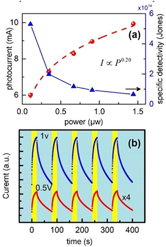
Figure 42. (a) Power-dependence of the photocurrent and specific detectivity for the mesoporous GaN photodetector. (b) Time-dependence of the current for the mesoporous GaN photodetector. Reproduced from [246] with permission of The Royal Society of Chemistry.
Download figure:
Standard image High-resolution imageTable 16 compares the performances of various UV photodetectors.
Table 16. Performance comparison between different UV PDs.
| Photodetector structure | Switch ratio | Photo-responsivity (mA W−1) | Specific detectivity (J) | Ref. |
|---|---|---|---|---|
| MoS2/GaN | ~105 | 187 | 2.34 × 10¹³ |
|
| Ga2O3/GaN | 152 | 54.5 | 1.23 × 10¹¹ |
|
| CH3NH3PbI3/GaN | 5 x 10³ | 198 | 7.96 × 10¹² |
|
| GaN/Si NP pilar array | ~104 | 29.4 | — |
|
| n-GZO NRs/Por-GaN | ~105 | 230 | 2.32 × 10¹² |
|
| CoPc/Por-GaN | ~105 | 588 | 4.8 × 10¹³ |
|
| MSM on Por-GaN | ~105 | ~107 | 5.3 × 10¹⁴ | [246] |
| MSM on ZnO/Ag/ZnO/PET | ~103 | ~102 | — | [247] |
| MSM on ZnO thin film | ~103 | 27 × 103 | 8.5 × 10¹³ | [248] |
*Ref. [249] and refs therein.
It can be seen from table 16 that the photoresponsivity and the specific detectivity of the heterojunction photodetector developed on CoPc and porous GaN are better by at least a factor of around 3 than those of devices based on bulk GaN. The parameters of metal-semiconductor-metal (MSM) photodetectors based on porous GaN are orders of magnitude better than those of devices based on ZnO films. Note that data related to photodetectors based on heterojunctions and those based on MSM structures should be analyzed separately, due to different mechanisms of operation. Particularly, the maximum values of photoresponsivity of MSM detectors with mesoporous GaN are much higher as compared to values characteristic to heterojunction photodetectors. Photoresponsivities up to 10 kA W−1 are attained with such photodetectors, due to a large internal gain related to the trapping of photo-generated holes at the mesoporous GaN/metal contact interface, as mentioned above. A product of the gain and quantum efficiency up to around 105 has been reached [246].
The applications of porous semiconductors in the development of gas sensors have been reviewed with a main focus on porous Si [250]. The interest to porous semiconductors as prospective materials for chemical sensor applications became even more pronounced in the last few years. Figure 43 summarizes chemical sensor behavior of some porous semiconductor materials. The application of porous GaN electrodes as Ag(I) trace detector is illustrated in figures 43(a) and (b). It was shown that porous GaN electrodes can detect lower concentration of Ag(I) compared to traditional planar electrodes [251]. Under the optimum conditions, porous GaN electrode showed a linear voltammetric response in the Ag(I) concentration range from 1 to 100 ppb with the detection limit of 0.5 ppb.
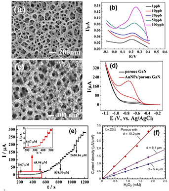
Figure 43. (a) SEM images of porous GaN. (b) Square-wave anodic stripping voltammetric determinations (SWASVs) of porous GaN electrode in acetate buffer solution containing 1, 10, 20, 50, 100 ppb Ag(I). Reprinted from [251], Copyright (2017), with permission from Elsevier. (c) SEM image of the AuNPs/porous GaN electrode. (d) Cyclic volammetric curves (CVs) of the porous GaN and AuNPs/porous GaN electrodes in 0.1 M PBS buffer containing 1 mM H2O2. Reprinted from [252], Copyright (2017), with permission from Elsevier. (e) Amperometric response curves for the addition of different concentrations of NaNO2 for the Pd-Pt/PGaN electrode in a 0.1 M PBS solution. Reproduced from [253]. CC BY 4.0. (f) Calibration plots of anodic currents versus concentration of H2O2 for porous InP samples with various pore depths (d). Solid lines indicate fitting curves obtained by least squares approximation. Reproduced from [254]. © IOP Publishing Ltd. All rights reserved.
Download figure:
Standard image High-resolution imageFigure 43(c) and (d) presents a non-enzymatic hydrogen peroxide (H2O2) sensor fabricated by electrodeposition of gold nanoparticles (AuNPs) onto porous GaN electrode obtained by photoelectrochemical etching of planar GaN [252]. The AuNPs/porous GaN electrode exhibited good electrocatalytic activity toward the reduction of H2O2 and performed as amperometric sensor for the detection of H2O2, demonstrating linear amperometric responses for H2O2 in the concentration range from 10 to 100 μM with the sensitivity of nearly 300 μA mM−1 and a limit of detection of 2 μM at a signal-to-noise ratio of 3. The cyclic voltammetric curves (CVs) display a current response of 220 µA for the AuNPs/porous GaN as compared to the 25 μA response of the porous GaN electrode without gold nanoparticles. These observations indicate that AuNPs play a major role in the electrochemical reduction of H2O2 in the sensor. It was shown that the AuNPs/porous GaN electrode exhibits good repeatability, reproducibility, selectivity and long-term stability for H2O2 detection. The detection limit of this sensor approaches that of a more complex sensor structure recently demonstrated on reduced graphene oxide (Pt/ZnFe2O4/rGO), used to modify the glassy carbon electrode [255].
The operation of a nitrite sensor fabricated by electrochemical deposition of palladium and platinum (Pd-Pt) nanocomposites on porous gallium nitride (PGaN) is demonstrated in figure 6(e). The sensor shows a detection limit lower than 1 µM, linear ampere response and high sensitivity of up to 150 µA mM–1 for nitrite, due to abundant electrocatalytic sites [253]. The sensor also showed good enough dynamic characteristics, indicated by the timely increase response towards every addition of NaNO2, and the steady state amperometric response attained in less than 3 s.
Another hydrogen peroxide (H2O2) sensor was demonstrated on the basis of porous InP nanostructures prepared by anodization in a HCl-HNO3 electrolyte [254]. All electrodes exhibit good linearity between the current signal and H2O2 concentration in a range from 0 to 2 mM (figure 43(f)). The highest current sensitivities for detecting H2O2 around 1.7 µA/mMcm2 was obtained on a sample with a pore depth d = 10.2 µm. The electrocatalytic activity of porous InP nanostructures functionalized by enzymatic molecules has been additionally investigated for application to amperometric biochemical sensors. A glucose oxidase (GOD) membrane was electrodeposited onto InP porous nanostructures to obtain amperometric glucose sensors [256]. Porous InP membranes with deposited Au nanoparticles were also shown to exhibit sensitivity to H2 and CO gases [52].
A hydrogen gas sensor on the basis of Pd Schottky contact on porous n-GaN was prepared by a low cost photoelectrochemical etching method [172]. This sensor exhibited a significant change of current upon exposure to different flow rates of 2% H2 in N2 gas as compared to the standard Pd/GaN sensor prepared on the as-grown GaN sample. The response increased exponentially with hydrogen flow rate for both sensors, but the Pd/porous GaN was found to be more sensitive to hydrogen than that based on the as-grown GaN (7 times more sensitive at a flow rate of 150 sccm). Apart from that, the response and recovery times were reduced for the Pd/porous GaN sensor as compared to the standard one (figure 44(a)).
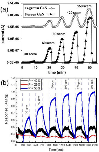
Figure 44. (a) The on–off currents of the porous GaN gas sensors operating at room temperature for a constant voltage of 1 V exposed to different hydrogen flow rates. Reprinted from [172], Copyright (2012), with permission from Elsevier. (b) Effect of porosity on H2 detection at room temperature versus time. Reprinted with permission from [257]. Copyright (2019) American Chemical Society.
Download figure:
Standard image High-resolution imageA detection limit of H2 at the level of few ppm was demonstrated at room temperature with a sulfur-treated, platinum (Pt) decorated porous GaN [257]. It was found that the sensing response of the gas sensor increases with the increase in porosity (figure 44(b)).
The performance of H2 gas sensors on the basis of porous GaN is compared in table 17 with that of sensors demonstrated on various ZnO nanostructures. The response of sensors was determined as (Ra − Rg)/Ra, where Ra and Rg are the electrical resistivity of the sensor in the presence of air atmosphere and hydrogen gas, respectively.
Table 17. Room-temperature H2 gas sensing performances of conductometric sensors based on porous GaN and ZnO nanostructures.
| Material system | H2 concentration (ppm) | Response | Ref. |
|---|---|---|---|
| Porous GaN 58% porosity | 30 | 0.50 | [257] |
| Hydrothermal ZnO nanorods | 500 | 0.52 |
|
| Microwaveassisted chemical solution ZnO nanorods | 1000 | 0.75 |
|
| ZnO nanoline prepared by soft e-beam lithography | 100 | 0.19 |
|
| ZnO:Pt | 1000 | 0.65 |
|
| ZnO:Mg | 100 | 0.36 |
|
| ZnO:La | 1000 | 0.51 |
|
*Ref. [258] and refs therein.
It can be seen from table 17 that none of ZnO based sensors demonstrate a better response at room temperature to H2 concentration lower than 100 ppm than those prepared on porous GaN. Moreover, the response of sensors based on porous GaN to 30 ppm of hydrogen is comparable with that of other sensors to 500 ppm or 1000 ppm hydrogen concentration.
A GaN-based two-sensor array for methane detection in an ethanol environment was fabricated by PEC etching of GaN layers in various solutions [259]. It was found that etching in a KOH solution results in a pyramidal morphology of the layer which exhibits a high sensitivity to methane gas, whereas etching in a H3PO4-based solution leads to the formation of individual nanoneedles with a high sensitivity to alcohol vapors. The gas sensitivity of GaN structures with different morphologies was investigated as a function of temperature and the cross sensitivity to humidity.
The sensitivity to humidity has been demonstrated with electrochemically made porous GaAs [260] and with a ZnO/porous GaN heterojunction [261]. The response of the metal/porous GaAs structure to the adsorption of water was attributed to the decrease in the bulk resistivity and potential barrier height formed at the Ag/PGaAs interface. The formation of a thin oxide layer was also observed on the surface of porous GaAs, which plays a dual role by increasing the ability to adsorb water molecules and by preventing the surface from degradation. Porous GaAs has an advantage of being more stable against degradation by water vapor as compared to porous silicon. Figure 45(a) shows the reaction of the sensor upon the exposure to water vapors, and the good recovery after introducing the air. It was shown that a full recovery of the initial signal can be achieved by a short heating of the sensor.
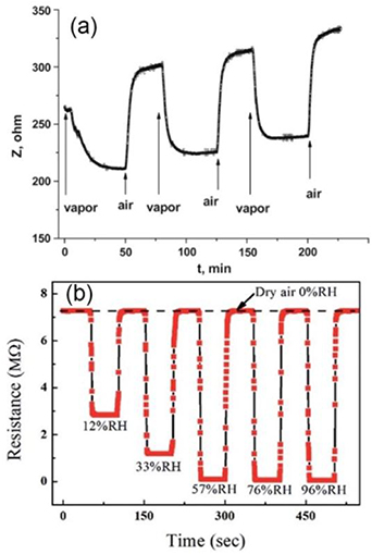
Figure 45. (a) Dynamic response signal of a Ag/PGaAs sensor on supplying of three cycles of saturated vapors of water at pumping through the bubbler at frequency 2 MHz. Reproduced from [260]. CC BY 3.0. (b) The dynamic humidity sensing behavior of the ZnO/PGaN based device. Reproduced from [261]. CC BY 3.0.
Download figure:
Standard image High-resolution imageThe ZnO/PGaN heterojunction [261] displays excellent diode properties and transport capability which contributes to enhanced electron transfer, high sensitivity and quick response/recovery time (7 s/13 s) under relative humidity levels in the range of 12%–96% RH. The sensitivities are 1.6; 5.2; 80.4; 123.6 and 161.0 at 12; 33; 57; 76 and 96% RH, respectively (figure 45(b)).
A comparison of the ZnO/PGaN performance with previous humidity sensors demonstrates better parameters in terms of response/recovery time with nearly the same measuring range and sensitivity [table 1 in 261].
5.5. Light emitting devices
The improved luminescence properties, in combination with possibilities to configure various optical cavities offered by electrochemical etching, open new prospects for implementing porous semiconductors in light emitting devices. Optical cavities can be produced on the basis of selective etching of GaN. It was shown that two regimes of etching with different etching characteristics can occur depending on the doping concentration and applied voltage, i.e. nanoporous and electropolishing [262], which provide tools for fabrication of novel optical and microelectromechanical-system devices. GaN microdisks and distributed Bragg reflectors were fabricated by this technology (figure 46(a)). Stimulated emission of GaN microdisk was observed under pulsed optical pumping (figure 46(b)). Optical modes with the linewidths much less than that inherent to the near bandedge emission (~5 nm) are clearly observed from the optical microcavity with pumping higher than the threshold. The spacing between the optical modes agrees well with whispering gallery mode (WGM) lasing. The linewidth is less than 1 nm, similarly to the WGM modes observed from high quality ZnO microrods [263] and ZnO microdiscs [264], indicating the quality factor higher than 500. However, the quality factor of the cavity can be significantly improved, since the roughness (~10 nm) of the microdisk sidewall was not optimized.
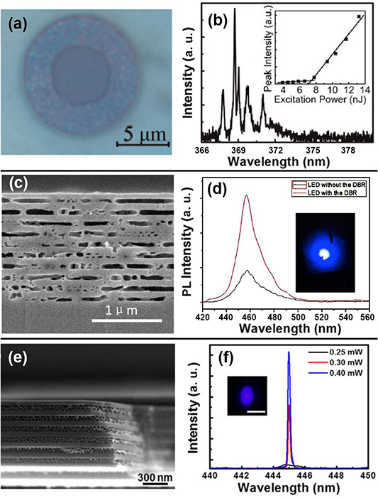
Figure 46. (a) Optical microscope image of the GaN microdisk with a nanoporous layer. (b) Light emission spectrum from an optically-pumped GaN disk after threshold. The inset shows the emission intensity versus excitation power. [262] John Wiley & Sons. Copyright © 2010 WILEY-VCH Verlag GmbH & Co. KGaA, Weinheim. (c) Cross-sectional SEM images of the NP-GaN DBRs structure produce by electrochemical etching of an undoped GaN/n-type GaN periodic structure. (d) Room temperature PL spectra of the LED structures grown with and without the NP-GaN DBRs structure under the excitation with 405 nm wavelength. The inset shows light emission of the LED with the NP-GaN DBR by current injection. Reprinted from [265], Copyright (2018), with permission from Elsevier. (e) Cross-sectional SEM image of a GaN/NP-GaN DBR structure used as bottom mirror. (f) Output spectra at different excitation powers (below, at and above threshold) originated from an optically pumped micro-cavity with a GaN/NP-GaN bottom DBR and a dielectric top DBR. Inset is far field laser spot from optical pumping of the micro-cavity (scale bar is 5 mm). Reprinted with permission from [266]. Copyright (2015) American Chemical Society.
Download figure:
Standard image High-resolution imageAnother light emitting device was demonstrated on a wafer-scale distributed Bragg reflector (DBR) structure consisting of lattice-matched polar (0001) GaN and nanoporous GaN layers fabricated by electrochemical etching of an undoped GaN/n-type GaN periodic structure (figure 46(c)). InGaN-based light emitting diodes (LEDs) were regrown on the DBR templates [265]. The photoluminescence intensity of the LED structure produced on the etched template was found to be four times higher than for a standard LED (figure 46(d)).
A similar InGaN LED structure was grown on a DBR structure produced by doping-selective electrochemical etching process of a 12-period Si-heavily doped GaN/undoped GaN stack structure [267]. High electroluminescence emission intensity and line-width narrowing effect were measured in this DBR-LED compared with the non-treated LED structure. Additionally, resonant cavity effect was observed in the InGaN LED with bottom nanoporous-DBR and top GaN/air interface.
Apart from Si-doped GaN/undoped GaN stack structure, n+-AlGaN/undoped-AlGaN stack structures with different Al contents were used for the preparation of porous DBR reflectors by means of doping-selective electrochemical etching in GaN based UV LED structure [268, 269]. Reflectivity higher than 90% was achieved with such DBR reflectors at the working UV wavelengths. InGaN/GaN MQWs were replaced by GaN/AlGaN MQW active layers in such types of UV LED structures.
Vertical light emitting diodes with an active InGaN/GaN multiple quantum wells (MQWs) structure were also fabricated via a process designed to slice and separate the produced LED devices [270]. The process included electrochemical anodization to create nanoporous (NP) GaN of designed porosity profiles. The NP GaN has undergone shape transformation into a largely voided morphology during the overgrowth of the MQWs LED structures, therefore enabling large-area separation of the LED structures after appropriate wafer bonding. Finally, the blue emitting GaN LEDs were transferred to silicon substrates with vertical configuration by this unique process. Therefore, a versatile separation of LED layers without the aid of energetic laser raster, ion implantation, or the embedding of esoteric sacrificial layers was proposed. A similar lift-off method was applied to fabricate GaN vertical LEDs which were separated from the sapphire substrate and transferred to a Mo substrate [271].
To achieve laser action with such types of InGaN/GaN MQWs, a more complex structure consisting of three elements has been proposed [266]. By using possibilities to control the pore morphology of GaN from macro- to meso- and micro-Porous via the doping and electrochemical etching bias, optical engineering of a DBR with a record reflectance of (R > 99.5%) was demonstrated (figure 46(e)). This DBR was used as a bottom mirror for a more complex laser structure composed of three elements: (i) the bottom DBR mirror; (ii) a planar InGaN microcavity for optical pumping constructed from 10 In0.15Ga0.85 N (3 nm)/GaN (8 nm) quantum wells designed for luminescence wavelength (λPL = 450 nm); and (iii) a top dielectric mirror constructed from 12 pairs of dielectric SiO2/TiO2 layers. Single mode lasing at 445 nm with 0.17 nm linewidth was achieved above the threshold with such a complex laser structure (figure 46(f)). Quality factors of resonators comparable to those of high quality ZnO cavities have been reached with microcavities employing porous layers (table 18).
Table 18. Quality factors of microcavities produced with GaN and ZnO structures.
| Material | Resonator quality factor | Ref. |
|---|---|---|
| ZnO microrod | 400 | [263] |
| ZnO microdisc | 640 | [264] |
| GaN microdisc | >500 | [262] |
| GaN/Por-GaN microcavity with two DBR | 2600 | [266] |
| ZnO microrods | 2600 | [272] |
So, porosification of GaN by conductivity based selective electrochemical etching provides conditions for preparation of nanoporous GaN layers with controlled morphology and porosity, i.e. with decreased in a controlled manner refractive index, at the same time the crystallinity of the material being preserved. As a result, conditions are provided for replacing the AlGaN cladding layers used for two decades in the development of InGaN laser diodes. These new technologies based on porous layers preparation overcame the two basic limitations of AlGaN cladding layers, namely the epitaxial (strain) and optical (index) limitations. It was shown that compared to Al0.1Ga0.9GaN cladding, which has a refractive index contrast (Δn) ~0.04 to GaN, the Δn of NP-GaN to GaN can be engineered to be over 0.4 without inducing any tensile strain [273]. The high Δn value offered a broad tunability of the confinement factor (Γ) and the modal gain in edge emitting InGaN laser diodes as compared to the state of the art ones. It was found that the increase of the Γ leads to a more than two-fold reduction of the lasing threshold under optical pumping.
Apart from producing classical optical cavity resonators, electrochemical etching proved to be suitable for the development of random laser media, since the physical mechanism of optical confinement in such media is based on the formation of ring microcavities in a micrometer-scale random medium due to the strong scattering of the light. Random laser media based on porous semiconductors provide some advantages as compared to traditional powders, nanocrystallite clusters, and disordered organic materials [274–276], since they are suitable for integration with other optical or electronic functions. Electrochemical porosification provides instruments for preparation of light scatterers of different shapes, morphologies and sizes by combining different regimes of semiconductor material dissolution resulting in crystallographically oriented or current line oriented pores as described in the previous sections. Even more opportunities are provided in this sense by the fabrication of two-phase composite nanostructures based on porous semiconductor matrices, assuring the highest contrast of the refractive index and the optimum scattering properties.
Random lasing emission was demonstrated from the microporous surface of a Cr2+:ZnSe crystal [277]. A random lasing emission with a center wavelength of 2350 nm and laser-like threshold of 0.3 mJ/pulse was observed under 1750 nm excitation of Nd:YAG (355 nm) pumped optical parametric oscillator (figure 47(a)). The random lasing behavior based on microporous surface of Cr2+:ZnSe crystal was found to occur for a wide pump wavelengths ranging from 1500 nm to 1950 nm, which is in accordance with the optical absorption characteristics of Cr2+:ZnSe crystal. A series of composite materials prepared on the basis of porous semiconductor GaP, GaAs, and Al2O3 templates doped with rare earth elements and transition metals have been analyzed from the point of view of random lasing action [178]. As described in section 3, a series of composite materials containing Ga2O3, GaPO4, ErPO4, EuPO4, ErAsO4 and EuAsO4 nanophases are formed depending on the technological conditions applied. It was suggested that each of the considered composite materials has specific advantages and disadvantages from the point of view of the inset of laser action. The rare earth ions incorporated in the prepared composites, which represent a quasi-four level laser medium, were suggested to be much more efficient than the three level laser medium of Cr3+ ions. On the other hand, the efficiency of incorporating the rare earth ions into the matrices of Ga2O3, GaPO4 or Al2O3 is low due to their large radii, in contrast to Cr3+ ions. From this point of view, it was concluded that the best choice is doping with Ti3+ ions, for instance in porous Al2O3 annealed at high temperatures.
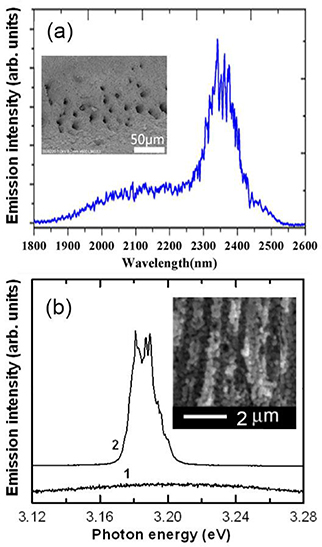
Figure 47. (a) Emission spectra of microporous surface of Cr2+:ZnSe crystals with 1700 nm pump wavelength and 1.6 mJ/pulse pump energy. The inset shows the SEM micrograph of pump area. Reprinted from [277], with the permission of AIP Publishing. (b) Emission spectrum of a porous ZnO sample measured with the excitation power density of 1.2 MW cm−2 (1) and 5.7 MW cm−2 (2). The inset shows the SEM micrograph of a porous ZnO sample produced by annealing of a ZnSe template. [178] John Wiley & Sons. Copyright © 2009 WILEY-VCH Verlag GmbH & Co. KGaA, Weinheim.
Download figure:
Standard image High-resolution imageApart from doping with rare earth elements and transition metals, making use of laser media with intrinsic optical gain properties based on near-bandgap electronic effects in semiconductors (exciton-exciton scattering or electron-hole plasma), is another way to realize stimulated emission [153, 178]. This approach was demonstrated by transforming a porous ZnSe template, preliminarily prepared by electrochemical treatment of a ZnSe single crystal, into a porous ZnO medium via a procedure of thermal treatment (see figure 26, and the inset in figure 47(b)). Random laser action was observed in such a medium with a threshold of 5 MW cm−2 at room temperature under the excitation by nsec laser pulses from a third harmonic Nd:YAG laser (figure 47(b)).
5.6. Photonic engineering: waveguides and Bragg reflectors
As seen from the above analysis, waveguides and Bragg reflectors are among key elements in porosity-based photonic engineering. Particularly, they are important for the development of LEDs [265–269, 273], while their areas of applications are much broader.
A waveguide was prepared with nanoporous GaN as the cladding layer underneath the GaN core layer [273]. The NP-GaN cladding layer was produced by electrochemical etching conducted by applying an anodic bias on the sample in an acidic electrolyte. Strong transverse waveguiding was achieved with such NP-GaN as the cladding layer underneath the GaN core layer with three InGaN quantum wells (3 × 3.5 nm) and air as the top cladding layer. The modal gain investigation of the waveguide by means of the variable stripe length (VSL) method revealed net modal gains of 32.7, 46.0, and 70.6 cm−1, for three samples with a confinement factor (Γ) of 4%, 6%, and 9%, respectively, with pumping at 1.07 MW cm−2. The material loss α of the entire waveguide, including both the absorption from GaN waveguide layers and the optical scattering loss due to the nanoporous n+-GaN cladding was estimated to be lower than 1 cm−1 at the wavelength of 430 nm, which is indicative of the great promise of using NP-GaN as a low-loss epitaxial medium for III-nitride photonic engineering.
Possibilities to excite guided wave modes into porous GaN have been demonstrated via the control of the refractive index of GaN films and its birefringence by adjusting the pore sizes and film density [278]. The electrochemical etching process was optimized in order to get porosities from 0 to 40%. Guided wave modes were systematically investigated by prism coupling.
Waveguides were also produced by engineering the morphology of porous structures in n-InP [279, 280]. As described in section 3, lithographic patterning of the sample surface before anodic etching modifies considerably the electric field distribution which, in turn, defines the direction of pore growth inside the specimen. Waveguides were produced by introducing current-line oriented pores which grow in radial directions from nucleation layers defined by lithographic patterning (see figure 18(b)). At the same time, it was shown that switching from curro to crysto pores results in the formation of Bragg-like structures by alternating high refractive index with low refractive index porous layers [31]. Porous superlattices consisting of a stack of alternating two layers with various morphologies and porosities suitable for photonic applications have been produced by periodically changing the applied current or potential in acidic solutions [280].
DBRs with peak reflectance greater than 98% at 450 nm with a stopband width of 72 nm have been fabricated by electrochemical etching on free-standing nonpolar m-plane GaN substrates consisting of alternating pairs of undoped and highly n-type-doped GaN layers [281]. It was found that the bias voltage controls the average pore diameter, while the pore density is primarily determined by the doping concentration. The volume average theory (VAT) was applied to the digitized SEM images to determine the index of refraction and porosity for samples etched with different bias voltages. The deduced porosity and index of refraction are presented in figure 48. The data have been verified with a semi-empirical approach using the transmission matrix method (TMM) applied for fitting the measured reflectance spectra. It was shown that the nanoporous DBRs maintain the polarization of a polarized source upon reflection. Such kinds of DBRs are destined to the development of polarization-pinned nonpolar VCSELs with higher output power.
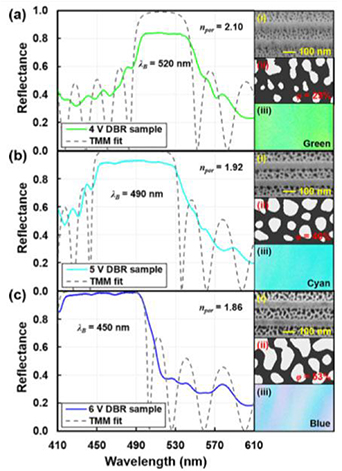
Figure 48. Reflectance spectra of the nanoporous DBRs fabricated using three different bias voltages (a) 4 V (green), (b) 5 V (cyan), and (c) 6 V (blue) and TMM fits using VAT (dashed curves). The side images show the (i) magnified SEM cross-section images, (ii) VAT digitized images, and (iii) top-down microscope images of the corresponding DBR samples. Reprinted from [281], with the permission of AIP Publishing.
Download figure:
Standard image High-resolution imageApart from high reflectivity and low absorption of DBRs, good conductivity is highly desirable for many device applications. The wafer-scale fabrication of non-polar GaN/mesoporous GaN DBRs exhibiting high peak reflectivity (>96%) across the entire visible spectrum, wide spectral stop-band widths (full-width at half-maximum >80 nm), good material quality and electrical conductivity have been demonstrated by a facile one-step electrochemical etching method without any extra processing steps [142].
While most of the DBRs have been fabricated on alternating n-GaN and nondoped GaN layers prepared by MOCVD [142, 265–269, 273, 281], DBRs structures have also been demonstrated on GaN bulk substrates grown by HVPE [135]. It was shown that HVPE-grown GaN bulk substrates are intrinsically suitable for producing multilayer porous structures (MPS), without any additional technological procedures for growing layers with controlled conductivity, as in the case of MOCVD growth of GaN. As described in section 3, the HVPE-grown GaN wafers were found to consist of domains with a 3D modulation of electrical conductivity formed due to peculiarities of the HVPE growth which involves generation of pits and their overgrowth [44]. These domains are constituted of sheets with alternating conductivity, which are suitable for producing MPS during the anodization (see figure 22(a)). The composition of electrolytes, their concentration and the anodization potential applied during electrochemical etching were among technological parameters optimized for designing MPS suitable for Bragg reflector applications. A comparative study of electrochemical processes for the preparation of MPS was performed on HVPE and MOCVD-grown GaN [134]. The feasibility of the produced structures for the design of Bragg reflectors or other photonic elements has been demonstrated by micro-reflectivity measurements accompanied by transfer matrix analysis and simulations by a method developed for calculation of optical reflection spectra.
The parameters of light emitting and other optoelectronic and photonic devices are to a large extent determined by the reflectivity of the used DBR. Table 19 compares the reflectivities of various DBR.
Table 19. Reflectivity of various DBR.
| Material system | Peak BDR reflectivity (%) | Ref. |
|---|---|---|
| 12 pairs Nanoporous GaN/undoped GaN | 97.1 | [267] |
| 10 pairs Nanoporous GaN/undoped GaN | 99.5 | [266] |
| 15 pairs Nanoporous GaN/undoped GaN | 98.7 | [281] |
| 10 pairs Mesoporous GaN/undoped GaN | 96 | [142] |
| 12 pairs Por-AlGaN/undoped AlGaN | 93 | [269] |
| 5 pairs Nanoporous TiO2/dense TiO2 | 95.1 | [282] |
| 29 pairs AlN/GaN | 99.4 | [283] |
| 8 pairs Ta2O5/SiO2 | 99 | [283] |
| 40 pairs AlGaN/GaN | 91.6 | [284] |
| 40 pairs AlInN/GaN | 99.7 | [285] |
| 6 pairs SiO2/HfO2 | 97 | [286] |
| 25 pairs GaAs/AlGaAs | 97.3 | [287] |
| Double–8 periodsTiO2/SiO2 | 95.1 | [288] |
| 20 pairs ZnTe/ZnSe | 98 | [289] |
| 25 pairs AlGaN/Ag | 90 | [290] |
| 50 pairs AlGaN/Ag | 99 | [290] |
The analysis of data in table 19 shows that reflectivity higher than 99% is reached with DBR based on nanoporous GaN, while similar reflectivity with epitaxial layers of other material systems are achieved with much larger number of pairs. Apart from that, epitaxial layers are usually grown by costly MBE equipment.
Development of optical elements capable to focus the electromagnetic radiation is an important issue to achieve integration in optoelectronic and photonic circuits. Photonic crystal structures made from porous dielectrics provide instruments for developing various lenses, including the ones with super-resolution [291], while electrochemical etching of semiconductors can ensure conditions for the formation of photonic crystals structures, as demonstrated by the preparation of a single crystal of nanopores [144]. Good focusing effect was proved with a photonic crystal concave lens made of porous dielectric, working both in the long wavelength limit where n> 1 and in the spectral regions characterized by negative refractive index [292].
Even more opportunities for designing photonic crystal lenses are provided by metalizing the porous semiconductor structures [57]. The focusing properties of flat lenses assembled from metallized porous structures or by clusters of metallized ZnSe and TiO2 nanotubes were studied by calculating the transmitted through the lens the electromagnetic power T=(E/E0)2, where E is the electric field amplitude of the radiation passed through the lens, and E0 is the electric field amplitude without the lens [57, 293, 294].
It was revealed that the focusing properties of a photonic flat lens assembled from clusters of metalized ZnSe nanotubes with the inner diameter of 40 nm and the wall thickness of 20 nm with a design illustrated in figure 49(b) are better than those of a similar lens made of a porous ZnSe slab with regular arrangement of pores with the diameter of 40 nm and the wall thickness of 40 nm (figure 49(a)), both the pores and the nanotubes being metallized with a 6 nm thick Ag film. It was found that the photonic properties of metalized porous and nanotube structures are determined by both the arrangement of nanopores or nanotubes and their geometrical parameters. By decreasing the diameter of pores or the inner diameter of nanotubes by a factor of 2, the function of the photonic slab can be changed from a focusing lens (figures 49(a) and (b)) to a beam splitter (figures 49(c) and (d)).

Figure 49. (a) Electric field intensity map of a cross-sectional view of the 2D source-image system at the photon energy of 1.48 eV when imaging by a triangular-lattice photonic crystal flat lens consisting of metallized ZnSe pores with the diameter of 40 nm. (b) The same, but for a slab assembled from clusters of metalized ZnSe nanotubes with the inner diameter of 40 nm. (c) Electric field intensity map of a cross-sectional view of the 2D source-image system at the photon energy of 1.45 eV when imaging by a photonic slab with pore diameter of 22 nm. (d) The same, but for a slab assembled from clusters of metalized ZnSe nanotubes with the inner diameter of 22 nm. (e) Electric field intensity map of a cross-sectional view of the 2D source-image system at the photon energy of 1.39 eV when imaging by a photonic slab assembled from metalized titania nanotubes arranged in a triangular-lattice. (f) The same, but for a slab assembled from clusters of metalized titania nanotubes arranged in a superlattice.
Download figure:
Standard image High-resolution image
For comparison, figures 49(e) and (f) present the calculated imaging properties of photonic slabs assembled from metalized titania nanotubes arranged in a triangular-lattice or in a superlattice of nanotube clusters, respectively. The calculations were performed for titania nanotubes with the inner diameter of 80 nm and the wall thickness of 40 nm covered by a 12 nm thick Ag film. It can be seen that the sample with regular arrangement of titania nanotubes focuses the radiation similarly to the flat lens made of porous ZnSe with the triangular-lattice arrangement of pores, but the focus is at a larger distance from the lens, while the sample with clusters of titania nanotubes arranged in a superlattice demonstrates clear superlensing effect, i.e. S/λ2 < 1, where S is the surface of the focal spot and λ is the radiation wavelength (~0.9 μm).
The performed analysis demonstrates that the photonic properties of porous structures can be modeled by tailoring the arrangement of pores into clusters. However, the preparation of porous structures with such morphologies is more complicated from the technological point of view.
Templated fabrication of metal nanotubes by electrochemical pulsed deposition of Pt in InP and ZnSe porous layers with pore diameters from 40 to 400 nm was reported [57]. Ordered two-dimensional hexagonal arrays of pores were produced in n-InP crystalline substrates, and a uniform distribution of pores was realized in n-ZnSe substrates. Apart from fabrication of porous structures with pores directed perpendicularly to the template surface, the possibility to fabricate arrays of pores and networks of embedded metal nanotubes oriented parallel to the top surface of the template was demonstrated.
Two-dimensional metallo-semiconductor networks have also been fabricated by pulsed electrochemical deposition of Pt inside porous GaP membranes with parallel pores possessing diameters in the micrometer and sub-micrometer ranges, which are suitable for photonic and optoelectronic applications [125, 126].
Suspended ~15-nm thick GaN membranes nanoperforated in an ordered fashion have been fabricated using direct writing of negative charges by a focused ion beam and subsequent photoelectrochemical etching of GaN free-standing templates [295]. It was shown that the nanoperforated GaN membranes exhibiting a triangular lattice arrangement of holes with a diameter of 150 nm represent an intermediate case between 2D and 3D photonic crystals. The occurrence of two types of modes (surface and bulk modes) was found in such membranes and the prospects of their incorporation in photonic and optoelectronic integrated circuits were discussed. The technologies applied for the fabrication of photonic crystal structures based on GaN nanomemranes and their prospects for applications in photonic devices, sensors, microoptoelectromechanical and nanoelectromechanical systems, taking into account advantageous piezoelectric, optical, and mechanical properties of GaN and related III–V nitride materials, have been highlighted in a separate review [296].
While most of the ordered semiconductor nanostructures prepared by electrochemical etching are based on self-organization processes or on using surface charge lithography (as in the case of GaN nanostructures [295, 297]), hexagonal close-packed 2D photonic crystals were formed by electrochemical growth of CdSe through the interstitial spaces between polymer nano/micro sphere templates [298]. In such a case, the confocal voids containing photonic crystals can be made either interconnected or well separated, with high uniformity. It was suggested that the prepared 2D photonic crystals open wide opportunities for waveguide applications as distributed photonic scatterers, as well as active photonic elements obtained by filling the produced structures with optically sensitive materials.
6. Conclusions and outlook
The performed analysis demonstrates that the top-down approach of electrochemical nanostructuring of compound semiconductors has been gaining momentum over the last few decades. Possibilities for the fabrication of porous III–V and II–VI compound structures were developed. It turns out that some new types of pores and new physical properties are inherent to porous semiconductor compounds as compared to porous Si and Ge. Moreover, new mechanisms of the pore growth evidenced in III–V semiconductors, as a feedback, were later on brought to light in porous Si too, at a closer look.
A most prominent feature of pore growth in semiconductor compounds is related to complex processes of self-organization, which results in ordered arrangements of pores. These features, alongside the variety of compositions of semiconductor compounds, ensure large possibilities for the fabrication of ordered porous structures of different dimensionality without the use of costly lithography. On the other hand, the electrochemical formation of porous structures may be considered as a first step towards obtaining a large variety of other structures, such as nanowalls, nanoribbons, nanomembranes, nanowires, nanotubes, etc, within the same cost-effective electrochemical routs. Nevertheless, there is still plenty of room for investigating and understanding in more detail the complex system dynamics behind current oscillations in the process of pore growth, to keep under better control the self-organization processes that would ensure fabrication of porous structures with the needed design. Particularly, not all the possibilities to control the growth of ordered structures by means of external modulation of amplitudes, frequencies, and time sequences were explored in both galvanostatic and potentiostatic modes of electrochemical etching.
It remains to be understood why no crystallographically oriented pores are generated in II–VI compounds and solid solutions, while they have the same sphalerite crystal structures as the III–V compounds. Actually, these issues were analyzed just in terms of iconicity differences. It should also be elucidated why no current oriented pores grow in GaAs. In spite of the fact that the metal-assisted electrochemical etching is a cost-effective and versatile tool for the preparation of porous structures, its exploration is still in the primary phase.
As such, the top-down approach of nanostructuring is less expensive, versatile and not requiring sophisticated technologies and costly equipment, as compared to the bottom-up approach. Even more prospects for application are provided by a combination of the two approaches for the preparation of composite materials, when the porous templates are prepared by top-down electrochemical etching, while the second constituent of the nanocomposite material is introduced inside the porous template by the bottom-up electrochemical deposition. In this sense, not all the possibilities have been exploited for the plasmonic applications by depositing metal nanodots into porous semiconductor compound templates, or for photonic applications when the metallic nanodot arrays are assembled into nanotubes inside the template.
The doping of porous semiconductor templates with rare earths, transition metals and other elements, as well as the preparation of multiphase nanocomposites for random laser applications was just demonstrated experimentally, but no exploited. This is another wide field for exploration. Particularly, it is expected that the incorporation of some degree of order into an active random laser medium would reduce the random laser threshold. The combination of random lasing with photonic bandgap effects is also an important field for exploration. Some possibilities to control the degree of order in a porous semiconductor template have already been demonstrated, as discussed in the review.
Wide prospects for photonic applications would be opened by developing technologies for assembling locally configured porous clusters and their ordered arrangement on a large scale, as suggested by numerical calculations. However, this is a more complicated task as compared to reaching just ordered arrangement of pores, and more efforts of cross-disciplinary research are needed, combining semiconductor physics, electrochemistry, stochastic physics/chemistry, electrodynamic theory and the electromagnetic theory of light, nonlinear and quantum optics, etc.
Though the analysis in this review was restricted to electrochemical pore etching, it is not the only technique to produce porous materials. The combination of electrochemical technologies with other techniques, particularly with thermal deformation of pores and selective area sublimation, which have gained momentum over the last few years, could be an interesting approach for enlarging the technological tools for the preparation of nanostructured semiconductor compounds.
As concerns the variety of semiconductor compound compositions, in a temporal frame, since the year of 2000, electrochemical nanostructuring of III–V (InP, GaAs, and GaP) compounds was most intensively investigated. Later on, II–VI compounds and GaN started to be more actively involved, and an explosion in publications devoted to porous GaN has occurred during the last few years. In this regard, attention should be paid in the next few years to enlarging the variety of compositions via a more intensive exploration of III-Nitride compounds, solid solutions, and possibly diamond related materials, if the problem with the control of conductivity of these materials is solved.
Concerning applications, optical phononic engineering was explored in porous GaP, InP, GaAs and ZnSe compounds, while surface enhanced Raman scattering was mostly demonstrated in platforms of porous GaN with metal inclusions. Nonlinear optical properties were explored for second harmonic generation and THz emission in porous GaP and InP. The problem of phase matching for second harmonic generation in isotropic materials can be solved by porosity induced artificial birefringence. These findings open wide prospects for making use of high values of the second order nonlinear optical coefficients of III–V compounds, which are several orders of magnitude higher than those of KDP, ADP and other materials traditionally used in upconversion. Photodetectors and sensors for environmental monitoring were demonstrated on porous GaN, InP and GaAs. Prospects for implementing in energy storage and photocatalytic applications were disclosed in the case of porous CdS, CdSe, ZnSe, GaAs, ZnO and GaN compounds.
While waveguides and photonic crystals based on single crystals of pores have been demonstrated in porous InP and GaP, mostly porous GaN structures were practically implemented in concrete photonic engineering applications. The most impressive of them are based on Bragg reflector structures. Nevertheless, porous GaN and related materials have a great potential for a wider implementation in structures and superstructures for hybrid photonic, quantum photonic, optoelectronic, optomechanic, piezoelectric microelectromechanical (MEMS) and piezo/acoustophotonic devices, by making use of advanced electrical, photonic, piezoelectric and mechanical properties of GaN and related materials.
However, to reach these goals, the problem of producing bulk GaN crystals with high homogeneity and uniformity of electrical properties should be solved. Nowadays, HVPE growth appears to be the best choice among the three main technologies used for GaN bulk crystal growth: HVPE, sodium flux and ammonothermal growth. Note that achieving a highly uniform conductivity throughout the bulk GaN is still challenging, since the formation of V-shaped defects or pits leads to the generation of extended inhomogeneities upon subsequent overgrowth, as discussed in this review. Overcoming this challenge would open new opportunities for the exploration and exploitation of self-organized processes occurring in GaN subjected to electrochemical or photoelectrochemical etching.
Acknowledgments
The authors acknowledge financial support from the Ministry of Education, Culture and Research of Moldova under the Grant #20.80009.5007.20. This work has received partial funding from the Horizon-2020 Spreading Excellence and Widening Participation research and innovation programme of the European Union under the grant #810652 (NanoMedTwin project). Eduard Monaico acknowledges support from the Alexander von Humboldt Foundation.