
Abstract
In this work, we have studied the multi-photon excited photoluminescence from metal nanoclusters (NCs) of Au, Ag and Pt embedded in Al2O3 matrix by ion implantation. The thermal annealing process allows to obtain a system composed of larger plasmonic metal nanoparticles (NPs) surrounded by photoluminescent ultra-small metal NCs. By exciting at 1064 nm, visible emission, ranging from 450 to 800 nm, was detected. The second and fourth-order nature of the multiphoton process was verified in a power-dependent study measured for each sample below the damage threshold. Experiments show that Au and Ag NCs exhibit a four-fold enhanced multiphoton excited photoluminescence with respect to that observed for Pt NCs, which can be explained as a result of a plasmon-mediated near-field process that is of less intensity for Pt NPs. These findings provide new opportunities to combine plasmonic nanoparticles and photoluminescent nanoclusters inside a robust inorganic matrix to improve their optical properties. Plasmon-enhanced multiphoton excited photoluminescence from metal nanoclusters may find potential application as ultrasmall fluorophores in multiphoton sensing, and in the development of solar cells with highly efficient energy conversion modules.
Export citation and abstract BibTeX RIS

Original content from this work may be used under the terms of the Creative Commons Attribution 4.0 licence. Any further distribution of this work must maintain attribution to the author(s) and the title of the work, journal citation and DOI.
1. Introduction
Plasmonic metal nanoparticles (NPs) have been intensively investigated in the last decades for a variety of technological applications in developing optical nanoscale devices [1], sensing platforms [2], light harvesting [3], second harmonic generation [4], metal-enhanced fluorescence [5, 6], among others. The plasmonic properties arise from the collective excitation of conduction electrons within the conduction band of noble metal NPs, known as localized surface plasmon resonance (LSPR). Plasmonic NPs have been found to lead a significantly near-field electromagnetic confinement in small volumes near the metal NPs [7]. In particular, these effects have been implemented to improve the photoluminescence (PL) emission from chromophores and quantum emitters [8, 9]. Apart from the extensive research on the enhancement of conventional one-photon excited PL, in the last decade, there exists a great interest in studying two-photon excitation PL enhanced by metal NPs [10–13]. This is an emission process that can take place when an emitter absorbs two photons of low energy simultaneously and emits a photon of high energy. This process can occur with two, three, four, or more photons, in which case, it is called multi-photon excited photoluminescence (MPEPL). The most common experiments involving multiphoton absorption are the excitation of emitters at infrared wavelengths and the subsequent emission at visible wavelengths. These phenomena have found promising applications in bio-imaging and bio-sensing thanks to the easy penetration of near infrared wavelengths into biological tissues and low photodamage under low-intensity laser radiation, and also in the development of photovoltaic solar cells with better efficiency at infrared solar radiation [14–18].
Even though MPEPL is most observed in chromophores, earth rare ions, and semiconductor quantum dots (QDs), a weak multi-photon induced luminescence has been also observed in larger plasmonic Ag NPs fabricated by lithography, where the physical mechanism is still unclear because the silver oxide plays an important role in the observed phenomena [19].
On the other hand, ultra-small metal nanoclusters (NCs) have emerged as a new kind of nanomaterials that have new optical properties different from those found in larger plasmonic NPs. Metal NCs do not have the quasi-continuum electronic density of states needed to support LSPR, and then the typical optical absorption peak signature does not appear in their absorbance spectra. Instead, metal NCs can absorb and emit light by PL, with their spectral characteristics depending on their size and composition, like it occurs for semiconductor QDs [20–22]. Size tunability properties due to quantum confinements make metal NCs advantageous over rare earth doped dielectrics [23]. Additionally, it has been shown that the size of the metallic cluster could be of few atoms (less than 0.5nm) up to 2 nm, a smaller size as compared with typical semiconductor QDs, but with low efficiency of about 1%–10%. The ultra-small size of the metal NCs, however, enables further miniaturization in solid-state photonic devices platforms compared to QDs. Moreover, metal NCs exhibits high photostability under high-power laser irradiation, providing photostable emission properties. This is in contrast to the photobleaching and blinking phenomena observed in QDs [24, 25].
Metal NCs are well characterized under one-photon excitation, but they also present nonlinear optical absorption properties such as multi-photon optical absorption, that could lead to MPEPL [26]. Recent works have reported that two-photon excited PL from QDs can be enhanced by coupling them to Au plasmonic nanostructures [12]. On the other hand, there is also a report on the observation of two-photon excited 25-times enhanced PL from colloidal Au NCs coupled to Au plasmonic nanorods [27].
With these motivations, in this work we have studied the MPEPL from Au, Ag, and Pt NCs surrounded by Au, Ag, and Pt plasmonic NPs, respectively, all embedded in sapphire matrices by ion implantation. The ion implantation technique enables the fabrication of a nanocomposite material consisting of metal nanoparticles embedded in a solid-state matrix, thereby enhancing nanocomposite's photostability and resistance to physical and chemical external damage. Some advantages of ion implanted nanoparticles, with respect to nanoparticles deposited by dewetting or chemical deposition, are their highly homogenous distribution and mechanical superiority regarding that their localization is inside of the matrix instead of over the surface. Additionally, this technique allows precise control over the elemental composition of the implanted ions, thus minimizing any detrimental effects caused by impurity atoms [28]. Another fundamental advantage of ion implantation is the versatility to couple nanoparticles in the same substrate by a well-controlled regulation of the deep of implantation. On the contrary, the cost could be signaled as a disadvantage. However, ion implantation is compatible with complementary metal-oxide-semiconductor technology. Then linear and nonlinear optical properties exhibited by the embedded nanoparticles can be directly applied in solid-state integrated photonics and optoelectronics devices for various applications such as signal processing, optical modulation, ultrafast optical switching, plasmon photovoltaic technologies, and sensing in the infrared wavelengths [29–32].
Following the implantation of metal ions into the sapphire matrix, thermal annealing promotes the nucleation and growth of the nanoparticles inside the sapphire matrix. The consequent nanocomposite consists therefore of both larger plasmonic NPs and ultra-small metal NCs embedded in the same implanted region. Since Pt NPs have a weak plasmonic response in the UV, then a very weak plasmon coupling, as compared with the one observed for Au and Ag nanoparticles, seems to be responsible for the experimental observations here reported. Power-dependent PL experiments, together with simultaneously nonlinear transmission measurements, were used to corroborate the multi-photonic process involved in the physical mechanism that explains the main experimental findings.
2. Experimental
Noble metals ions (Au, Pt, Ag) were implanted in fused silica (Suprasil 300) and sapphire (single crystal  -Al2O3) matrices of ultra-high purity by ion implantation (3 MV Tandem Pelletron facility at Instituto de Física, UNAM). Au, Ag, and Pt NCs inside silica or sapphire matrices were nucleated after ion implantation at 2 MeV and ions fluences of ∼
 as measured by Rutherford backscattering spectrometry (RBS). Table 1 summarizes the main results of RBS analysis for each sample. The chosen ion implantation fluencies are enough to produce a doped layer which stay above the supersaturation condition. According to the data in table 1, the atomic concentration can be estimated and ranged from
  ions cm−3, which is of the same order of magnitude for all the samples studied in this work. After the metal ions were implanted into the silica and sapphire matrices, the samples were thermal annealed at temperatures high enough to promote the mobility of the ions inside the matrix, and the consequent nucleation and growth of the nanoparticles. Au and Pt silica implanted samples were thermal annealed at 500 °C and 600 °C under a reducing atmosphere (RA) compound of 50%H2 + 50%N2 to nucleate ultra-small Pt and Au NCs inside silica matrices, respectively. These samples are labeled as Au-Sil and Pt-Sil. These temperatures for annealing were chosen to induce Au or Pt clustering, to recover the matrix from radiation damage, and also to passivate the irradiation-induced defect state in the silica matrix [33, 34]. Such annealing conditions have been optimized to obtain the highest photoluminescence for Au and Pt clusters. For the metal ions implanted in sapphire, the samples were thermal annealed under RA at 950 °C for 90 min for samples with Au and Ag ions, and at 1050 °C for the case of Pt ions. These samples are named as Au-Sap, Ag-Sap, and Pt-Sap. These thermal annealing conditions were chosen to produce a larger plasmonic response of the nanocomposite. Additionally, annealing temperature above 800 °C allows the passivation of optically active defects and the damage recovery induced by the ion implantation in sapphire [35]. The mobility of metal ions in sapphire is very high so the nucleation as a function of temperature and time starts immediately, and growth and ripening take place simultaneously. This results in the formation of ultra-small non-plasmonic NCs as well as very large plasmonic NPs. These broad size distribution inside sapphire matrices have been observed and studied before [36], and corroborated by our group using transmission electron microscopy (TEM) and optical studies [35]. The atomic concentration measured by RBS does not change after thermal annealing, then the estimated volume fraction of the NCs formed inside the silica samples is about 1.4%, and for NPs and NCs in sapphire is about 1.5%–2%.
Table 1. Ion implanted distribution in sapphire and silica: peak of depth under the substrate surface ( ) and their FWHM.
| Sapphire | Silica | |||
|---|---|---|---|---|
| Implanted Ions |
 (nm)
(nm)
|
 (nm)
(nm)
|
 (nm)
(nm)
|
 (nm)
(nm)
|
| Pt | 335 | 186 | 580 | 280 |
| Au | 329 | 187 | 570 | 282 |
| Ag | 520 | 251 | ||
Vertically polarized fundamental (1064 nm) and third-harmonic (355 nm) wavelengths from a 26 ps EKSPLA PL2231–50-SH/TH Nd:YAG pulsed laser System, with a repetition rate of 10 Hz (University Laboratory of Optics at Surfaces (Laboratorio Universitario de Óptica de Superficies) at Instituto de Física UNAM (LOS-UNAM), were used as pulsed excitation sources to perform single- and multi-photon PL measurements. The low frequency repetition rate and picosecond ultrafast laser pulses used in this work avoid possible effects of temperature rising on the PL emission from embedded metal NCs. Figure 1 shows the optical setup used in PL experiments and nonlinear transmission in input–output configuration. We use an Ocean Optics USB2000+ spectrophotometer previously wavelength-calibrated. Wavelength calibration was also checked by using a Deuterium–Tungsten Halogen Lamp DH-2000-BAL (Ocean Optics), and the varying output laser emission from an Optical Parametric Generator (PG401/SH-EKSPLA) through UV and visible wavelengths. Excitation with 355 nm laser pulses was performed below the ablation threshold of silica and sapphire matrices: ∼ 500 mJ cm−2 and ∼
 700 mJ cm−2, respectively. For 1064 nm laser pulses, the ablation threshold was of the order of 1.5–2.0 J cm−2 in single-shot irradiation mode. Single-photon excitation was performed by focusing a 355 nm spot laser of 3 mm of diameter, at normal incidence, and pulse energies of about 40–150
  J, i.e. irradiances up to 81 MW cm−2. High power excitation experiments at 355 nm were conducted for irradiances up to ∼
 10 GW cm−2. MPEPL experiments at 1064 nm were performed by using irradiances up to ∼
 GW cm−2. The nonlinear transmission of the metal NPs in sapphire was simultaneously measured by recording the input and output energy at various incident laser pulse energies, as it is also shown in figure 1. Optical absorption measurements were performed with a Varian Cary Spectrophotometer (Cary 5000). TEM micrographs in silica samples were obtained by using a FEI Tecnai F30 transmission electron microscope (FEG-TEM 300 kV) in Bright Field Mode. Microscopy observations of sapphire samples were obtained using 200 kV JEOL2010 FastTem FEG microscope in HAADF mode (Z-contrast). In both cases, TEM observations were carried out at a minimum resolution close to 1 nm. To prepare the samples for microscopy, they were mechanically polished from the side opposite to the ion implantation, in the direction normal to the sample surface, until a thickness of a few micrometers was achieved. In order to make the sample transparent to the electron beam, a Precision ion polishing system (PIPS) from Gatan company was employed to further thin the sample from the implantation side, resulting in a final thickness of less than 100 nm.
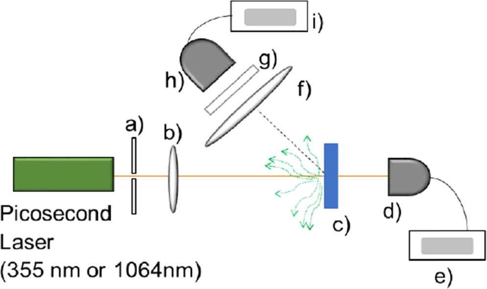
Figure 1. Optical setup to measure single and multi-photon excitation PL, and simultaneously the nonlinear optical transmission of the incident laser beam. (a) Aperture to collimate the laser beam. (b) Convex lens with a focal lens of 700 mm. (c) Sample mounted in an XYZ micrometric precision mounting. (d) High-power energy detector, and (e) its control. (f) Plano-convex lens with a focal length of 60 mm and a diameter of 25 mm. (g) Long (400 nm cut-off, 10LWF-400-B, Newport) or short (950 nm cut-off, 10SWP-950-B, Newport)-wave pass filter to block the scattering signal from the incident picosecond laser beam (355 nm or 1064 nm). (h) Optical fiber connected to a (i) spectrophotometer Ocean Optics USB2000+, which was used to collect the PL signal with an integration time of 1 s.
Download figure:
Standard image High-resolution image3. Results and discussion
Figure 2 shows a micrograph with Pt NCs in silica (Pt-Sil sample) with an average size of 1–3 nm. The experimental optical absorption for this sample is shown in figure 2(b), where the numerical fit, according to Mie theory, indicates an average size of about 1.8 nm. Numerical Mie calculations were performed using a plasma frequency size correction that can describe the vanishing resonance optical absorption of ultra-small metal nanoparticles [34]. The PL spectra from this sample, when excited at 355 nm or 1064 nm, are also shown in figure 2(b). As it is evident from this figure, the Pt-NCs in silica can emit light when excited at 355 nm, but not under excitation at 1064 nm. This PL emission from Pt NCs embedded in silica and sapphire has been observed before in previous works for low and high power laser excitation at 355 nm [21, 37]. The PL spectra of both Pt-NCs and Au-NCs have a broadband emission from 400 to 700 nm range, but the PL peaks are 532 nm and 547 nm respectively, i.e. the PL spectrum from Au-NCs is slightly redshifted. This broadband emission can be consequence of a broad size distribution of NCs inside the silica matrix [21, 27]. PL spectra of Pt and Au-Sil samples were also registered without using cut-off filters in the optical setup, and no PL emission is observed below 370 nm as it can be observed from the gray curve in figures 2(b) and (c). It is important to point out that the observed PL emission from the Au and Pt-Sil samples does not come from induced photo-active defect-states in silica after ion implantation. Structural photo-active defects-state induced in silica exhibit optical absorption bands near 250 nm, and they cannot be excited for excitation wavelength above 300 nm, as we have reported before [34]. The excitation wavelengths (355 nm or 1064 nm) used in this work are significantly distant from these optical absorption bands. Furthermore, as mentioned in the Experimental section, the thermal annealing above 500 °C under RA allows for a complete defect passivation.

Figure 2. (a) TEM micrograph in Bright Field Mode of Pt NCs embedded in silica by ion implantation (sample Pt-Sil). Absorbance and PL emission from (b) Pt-Sil and (c) Au-Sil samples. PL was measured after laser excitation at 355 and 1064 nm. The irradiances used in these experiments was of 20 MW cm−2 for excitation at 355 nm. For excitation at 1064 nm, irradiances ranged from 0.1 to 80 GW cm−2. Gray curves in (b) and (c) were taken without using the long wave pass filter in the optical setup.
Download figure:
Standard image High-resolution imagePt NCs behave as a quantum emitter for sizes below 2 nm. At this ultra-small size, the metal cluster cannot support plasmon resonance, typical of larger metal nanoparticles, because the electronic levels of these NCs become discrete. However, the metal NCs can absorb and emit light through the HOMO–LUMO orbitals that open an optical gap inside them. In figure 2(c), it is shown the PL emission from Au NCs in silica (sample Au-Sil) at 355 nm. The optical absorption spectrum does not exhibit any plasmon resonances, and the numerical fit shows that the mean size of the Au NCs is about 0.5 nm, small enough to have a discretized energy level, becoming thus a quantum emitter. Similarly, as for the case of Pt-Sil sample, no PL emission is observed when Au-Sil sample is excited at 1064 nm.
When exciting at larger wavelengths, such as 1064 nm, the photon energy is not enough to promote electrons through the HOMO–LUMO gaps of the NCs, then PL cannot be observed. However, at higher irradiances, it could be possible to observe PL emission at this larger wavelength by multi-photon absorption. Nonetheless, for the Pt-Sil and Au-Sil samples studied in this work, it was not possible to observe PL emission when excited at 1064 nm, even at irradiances as high as 80 GW cm−2. These results will be considered and tentatively explained below when the influence of the presence of NPs is considered.
Figure 3 shows the optical absorption of Pt, Au, and Ag-Sap samples. The absorption curves were numerically fitted by using the Mie theory, and the inset figure in each part shows the size distribution used to simulate the nanoparticle size distribution nucleated inside the sapphire matrices [34, 38]. We use the capability of MieLab software [38] in order to fit the proposed size distribution to the measured optical absorption spectra measured for each sample. For the Pt-Sap sample, the size distribution ranged from 1 to 6 nm, and the surface plasmon intensities in the UV peaked at about 280 nm. For the case of Au-Sap sample, the nanoparticle size distribution is broader, ranging from 1 to 40 nm, and the surface plasmon resonance is peaked at about 580 nm. Instead, Ag-Sap sample shows a size distribution ranged from 20 to 50 nm, with the presence of a large quantity of small NCs. The absorption band related to the LSPR of Ag-Sap sample is peaked at about 480 nm, being the most intense as compared to the LSPR measured for Pt-Sap and Au-Sap samples. Figures 4(a) and (b) show representative TEM micrographs of a sample with Au in Sapphire prepared under similar conditions as used in this work for the samples Au-Sap. As it can be appreciated, larger plasmonic Au NPs with sizes ranged from 4 to 40 nm in diameter simultaneously coexisted and are spatially overlapped with ultra-small Au NCs with sizes less than 2 nm, as shown in figures 4(a), (b) and the histogram from figure 4(c). On the other hand, figures 4(d) and (e) also show representative TEM micrographs of a sample with Ag nanoparticles synthesized under similar conditions as used in this work for the sample Ag-Sap. As it can be seen in figure 4(f), these samples show a wide size distribution of Ag nanoparticles ranged from 1.5 to 80 nm in diameter. These broader size distributions in sapphire samples have been corroborated in our previous works by TEM studies and optical analysis [21, 35], and it is consistent with the optical absorption spectra in figure 3 and its numerical fitting by Mie numerical calculations. TEM studies in figure 4 show that metal NCs are randomly distributed among larger plasmonic NPs. We can roughly estimate the volume density of NCs and NPs in sapphire samples by using atomic concentration and range measured by RBS and assuming a mean diameter for NCs and NPs according to TEM results. From Mie numerical calculation and TEM studies in figure 4 we can assume a NCs mean diameter of 2 nm, a mean diameter of 15 nm for Ag NPs, and 8 nm for Au and Pt NPs in sapphire. The estimated mean density for Pt, Ag, and Au NCs in sapphire is about  NCs
NCs  which corresponds to an inter-cluster mean distance of ∼
 nm. The estimated mean density for Au, Pt NPs in sapphire is about
  NPs
NPs  which corresponds to an inter-particle mean distance of ∼
 nm. While for Ag NPs in sapphire the estimated mean density is
  and a mean inter-particles distance of ∼
 70 nm. These rough estimations reveal that there could be randomly located several metallic NCs surrounding plasmonic NPs.
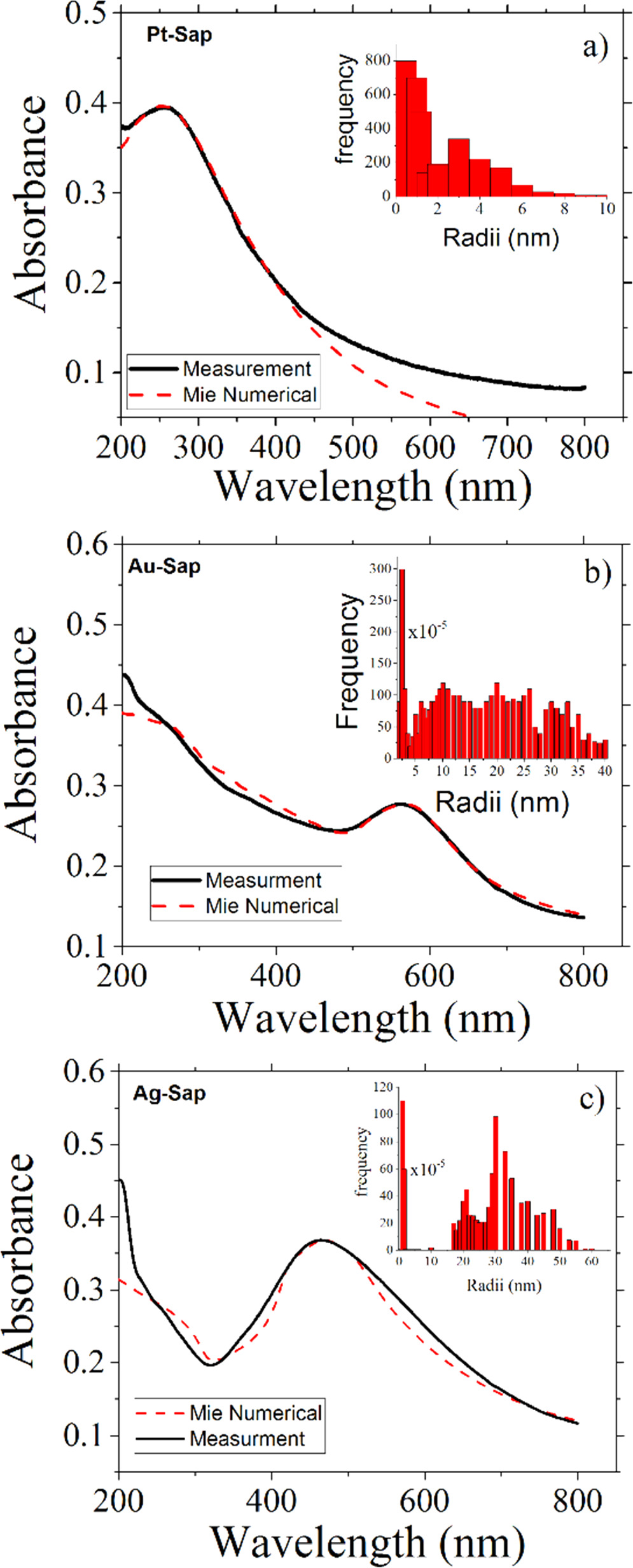
Figure 3. Absorbance of Pt, Au, and Ag nanoparticles embedded in sapphire by ion implantation (Continuous black curves). The red-dotted curves show the numerical fit performed by using Mie-type calculations. The insets show the nanoparticle size distribution used in each numerical simulation.
Download figure:
Standard image High-resolution image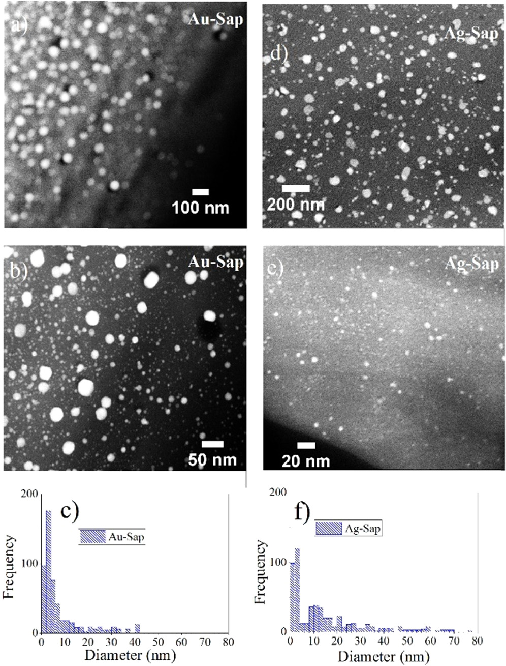
Figure 4. TEM micrographs in figures (a) and (b) were taken from a sample implanted with 2.5 × 10¹⁶ Au cm−2 and annealed at 1000 °C under RA. Images (d) and (e) were taken for a sample implanted with Ag in sapphire with 3 × 10¹⁶ Ag cm−2 and annealed at 1100 °C under RA. In both cases, TEM studies confirm the presence of Au and Ag nanoparticles and also reveal a wide size distribution, with larger NPs and ultra-small NCs of Au or Ag embedded in sapphire by ion implantation. Histograms shown in figures (c) and (d) show the size distribution obtained from TEM images of Au and Ag nanostructures, respectively.
Download figure:
Standard image High-resolution imageThe presence of ultra-small clusters gives rise to PL emission when the samples are excited at 355 nm, as it can be seen in figures 5(a) and (b). It is important to point out that this PL emission does not originate from optically active defect state in sapphire. Defect states in sapphire have been extensively studied, and most of them exhibit optical absorption band below 330 nm [35, 39]. In particular, the  color center has an absorption band at 361 nm, but its PL emission occurs at 380 nm [40], which falls outside the range of the observed PL emission from the samples studied in this work.

Figure 5. (a) PL spectra of Pt, Au, and Ag-Sap samples under excitation at 355 nm at low irradiances (20 MW cm−2) but without using the long wave pass filter in the optical setup. (b), (c) PL spectra of Pt, Au, and Ag-Sap samples under excitation at 355 nm at low and high fluence excitations (20 MW cm−2 and 10 GW cm−2, respectively). (c) PL spectra of Pt, Au, and Ag-Sap samples under excitation at 1064 nm and fluence of 61 GW cm−2. The cut-off due to the long wave pass filter is marked in each graph.
Download figure:
Standard image High-resolution imageThe PL spectra of sapphire samples can be seen in figure 5(a). This figure also shows the harmonic signal generated by the grating when the excitation laser enters into the spectrophotometer. The PL emission spectra in figure 5(b) show the PL signal from sapphire samples but filtering the harmonic signal. PL emission can be seen for both low (20 MW cm−2, figure 5(b) and high irradiances (10 GW cm−2, figure 5(c) at 355 nm excitation wavelength. At low irradiances the PL emission from Pt, Ag, and Au in sapphire can also be seen by the naked eye, as we reported before [21], but the PL of the sample with Pt has a lower intensity compared to that from Au and Ag samples. However, as laser excitation intensity at 355 nm increases, the PL from these samples exhibits superlinear PL dynamics, where the PL integrated intensity increases quadratically with the pump laser fluence [21]. Consequently, as it can be seen from figure 5(c), PL intensities are similar for all the metal NCs in sapphire, at higher power excitation of about 10 GW cm−2.
Comparing the PL emission from Au and Pt-Sil samples in figures 2 and 5 for Au and Pt-Sap samples, we observe that the PL spectra for Au and Pt-sap samples in figure 5 fall within the same spectral range (450–800 nm). Some differences in width, peaks, and intensities can be appreciated when comparing these results in both figures. However, it must be taken into account that the metal NCs in sapphire have different optical absorption properties, as shown in figure 3. These optical absorption properties result from the presence of larger metal NPs in sapphire samples. It indicates that the nucleation and growth processes under thermal annealing in sapphire are very different from those in the silica samples, leading to a different size distribution of both NCs and NPs. The difference in size distribution of NCs can modify the spectral width and intensities. Different NCs size distributions can explain the slight differences in PL emission properties, and for sizes above 2 nm the metal NCs does not emit light [21]. Additionally, as it is well known the presence of larger plasmonic NPs in sapphire can dramatically change the PL properties of the PL emitters as well.
In order to study the multi-photon absorption and PL excitations at infrared wavelengths, high laser irradiance was used, but at an excitation wavelength of 1064 nm (IR) with picosecond laser pulses. We considered that temperature rise by multi-pulse irradiation in NPs can promote peak shift, broadening or damping of the excited plasmon resonances [41]. However, ultrashort picosecond laser pulses in single shot pulse excitation can avoid these heating effects. The PL spectra measured in this case are shown in figure 6. Figure 6(a) shows the PL emission from sapphire samples under excitation at 1064 nm but without using the short wave pass filter in the optical setup, and the harmonic signal generated by the excitation laser entering into the spectrophotometer grating can be detected by the optical system. As it can be seen in figure 6(a), the PL spectra of all the samples is ranged from 400 to 850 nm. In figure 6(b) the laser is filtered by using a short-wave pass filter and the cut-off is marked in the graph. In contrast with the excitation at UV (355 nm) wavelength, at IR excitation, the PL intensity of the Pt-Sap sample is much less intense as compared to that from Ag-Sap and Au-Sap samples. The threshold irradiance from which it was possible to observe a PL emission at IR excitation wavelength was of 2, 5, and 40 GW cm−2 for Ag, Au, and Pt-Sap samples, respectively.

Figure 6. (a) PL spectra of Pt, Au, and Ag-Sap sample under excitation at 1064 nm and fluence of 61 GW cm−2 without using short wave pass filter. (b) PL spectra of Pt, Au, and Ag-Sap sample filtering the laser excitation at 1064 nm to avoid the harmonic signals.
Download figure:
Standard image High-resolution imageIn figure 5(c) all the samples exhibit a narrow peak at 690 nm after excitation at 355 nm. These peaks cannot originate from the laser system because the experimental setup has a long wave pass filter at 400 nm to avoid any reflection or scattering from the laser entering the spectrophotometer. A similar peak at 794 nm appears in figure 5(c), but only in the Ag-sap sample at an excitation wavelength of 1064 nm. These narrow peaks are likely a result of nonlinear plasmonic optical phenomena, as they manifest only under high-power excitation above 10 GW cm−2, and exclusively in the sapphire samples containing larger plasmonic NPs [21]. Similar optical effects can be observed in semiconductors QDs, and it is known as emission from exciton, or biexciton state for the case of two electron–hole pair generated inside NCs under high power excitation [42]. Transient excitonic responses have been observed in Ag surfaces and clusters [43]. However, further experimental studies are needed to precisely determine the physical origin of these narrow peaks in our samples, such as transient absorption spectroscopy or time-resolved experiments.
To know the excitation dynamics of the PL signal excited at 1064 nm, PL measurements as a function of the incidence energy excitation, below the ablation threshold measured for each sample (60–80 GW cm−2) at infrared (1064 nm) picosecond laser pulses, were performed. In figure 7(a) Log–Log plot of the PL intensity versus the incidence energy of the excitation picosecond laser pulses at 1064 nm is shown.
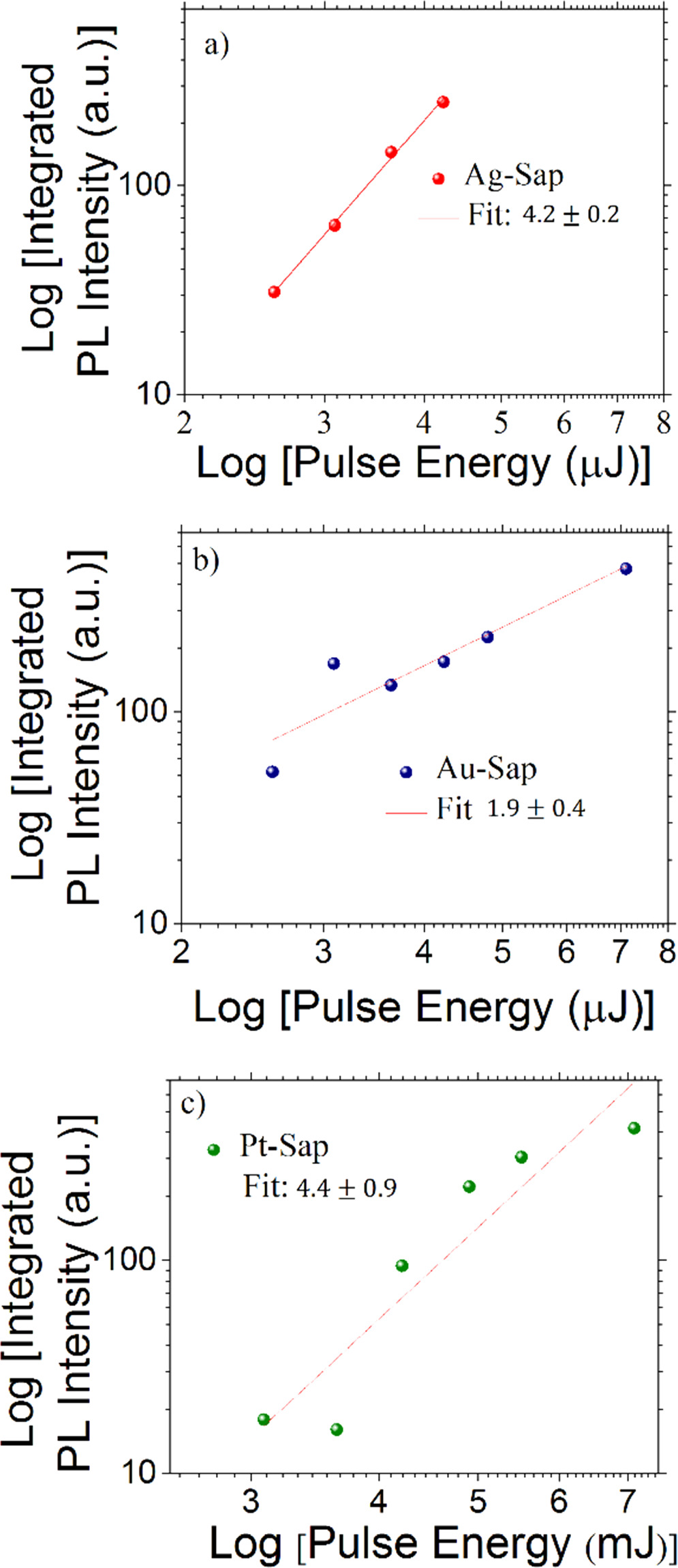
Figure 7. Power dependent PL integrated intensity from Ag, Au, and Pt-Sap samples excited with picosecond laser pulses (1064 nm).
Download figure:
Standard image High-resolution imageThe linear fitting in each case indicates the nature of the power dependence of the multi-photon absorption effect that gives rise to the PL emission in each sample. For the case of the Pt and Ag-Sap samples, the fitting is nearly 4, which means that we are observing an induced four-photon excitation PL process. Multiphoton photon excitation is a nonlinear process that scales with the two, three, or fourth power of the laser intensity for the simple case of single beam incidence. Particularly, in a multi-photon regime, a four-photon excitation process can also be described by a perturbative scaling proportional to the fourth power of the laser intensity [44, 45]. Instead, two-photon excitation PL occurs for the case of Au-Sap sample, as it is corroborated in the fitting in figure 7(b). These multi-photon absorption mechanisms were corroborated by executing simultaneously nonlinear transmission measurements, whose results can be seen in figure 8. At lower irradiances, the transmittances increase until reaching a maximum from which the transmittance monotonically decreases at higher pump power excitation due to a multi-photon absorption process. The nonlinear optical absorption (NLA) coefficient  can be estimated by adjusting the increase in transmittance and can be described by the following equation:

where  and
and  are the incident and transmitted irradiances, respectively.
  is the low irradiance absorption coefficient, and
  where
where  is the actual samples thickness. The linear absorption coefficient
  at 1064 nm was determined by using the laser pulses at low irradiances
  200 MW cm−2. The transmittance is defined as
  Equation (1) can be linearized in terms of
  so that the slope of the graph
  is equal to
  Then from the slope of the linear fitting in figure 8, the
  coefficient for each sample can be inferred. For Ag and Au-Sap, respective large values for
  1454 and 1170 cm GW−1, could be obtained. Instead, for Pt-Sap sample,
  is just 742 cm GW−1. Multiphoton absorption in NPs is originated when the probability that more than one photon should be absorbed by a single nucleus of absorption in a media. A lower value of
  means that for Pt samples it is needed a higher pump irradiance to observe multiphoton absorption process and consequently increase the probability of observing visible PL from Pt-Sap samples. The energy threshold from which a multiphoton absorption could be observed, is similar for each sample: 8.4, 5.7, and 6.7 GW cm−2 for Pt, Ag, and Au-Sap samples, respectively.

Figure 8. Picosecond nonlinear transmission at 1064 nm.
Download figure:
Standard image High-resolution imageIn table 2, the main results obtained in this work are summarized. The total power PL emission for the samples was estimated from the results in figures 2 and 4, considering the integrated PL intensity. As discussed above, laser excitation with picosecond laser pulses at 355 nm and 1064 nm can induce single-photon excitation (SPE) and multiphoton excitation (MPE) photoluminescence, respectively. The threshold energy to observe multiphoton optical absorption (NLA) and MPEPL is also tabulated in table 2.
Table 2. Data of total power PL emission for single-photon excitation (SPE) at 355 nm and MPE at 1064 nm,  NLA coefficient under infrared (1064 nm) picosecond excitations, and threshold irradiances for MPEPL and NLA.
| Sample | LSPR (Peak) (nm) | SPE power emission (nW) | MPE power emission (nW) | Threshold irradiance for MPE (GW cm−2) |
 (cm/GW) (cm/GW) | Threshold irradiance for NLA (GW cm−2) |
|---|---|---|---|---|---|---|
| Pt-Sil | nil | 3 a | nil | — | 21 [46] | 45 [46] |
| Au-Sil | nil | 2.9 a | nil | — | — | — |
| Pt-Sap | 255 | 23 b | 1 c | 40 | 742 | 8.4 |
| Au-Sap | 560 | 37 b | 3.8 c | 5 | 1170 | 6.7 |
| Ag-Sap | 460 | 36 b | 3.8 c | 2 | 1454 | 5.7 |
a Total power emitted for the same average laser excitation power of 1 mW. b Total power emitted for the same average laser excitation power of 44 mW. c Total power emitted for the same average laser excitation power of 180 mW. Cells space with '–' means that this quantity was not measured in this work.
As it can be seen in table 2, the power PL emission induced by MPE at 1064 nm of the Au and Ag-Sap samples is almost four times larger than that measured for the Pt-Sap sample. However, this PL intensity is 10 times lower than observed in the same samples, but under SPE by using an incident laser power four times lower.
On the other hand, for the case of Ag and Au-Sap samples, the threshold irradiance for NLA is a little bit higher than that measured for the MPEPL, and this slight difference can be attributed to the larger sensitivity of PL experiments. For the case of Pt-Sap sample, the differences for these threshold irradiances are much larger. These results suggest that even though the multi-photon absorption occurs in the sample with Pt nanoparticles at low power excitation, these phenomena do not activate the PL emission from the Pt NCs. However, at higher irradiance (>40 GW cm−2) the multi-photon PL emission could be observed.
Pt-Sil coefficient  values in table 2 were taken from our previous works in similarly prepared samples [46]. From the data in table 2, differences in the nonlinear response of the same metals in different matrices and different noble metals can be attributed to their electromagnetic contribution not only inside, but outside of the NPs. Remarkably, the stronger nonlinear optical absorption corresponds to the sample with an absorption peak closer to the double wavelength of excitation; it can be inferred that a two-photon absorption resonance occurs in the experiment. In this respect, the third-order nonlinear optical susceptibility
  responsible for nonlinear optical interactions of absorption can be considered to be a function of a detuning of frequency ω, related to the LSPR of the different NPs, and this detuning can be represented as Δ = ω − ω21 involved in the following expression [47]:

where  is the number of atoms per unit volume in the system,
  represents the Planck constant, and the atomic dipole moment is m. The magnitude
  is associated with the population loss through radiative and non-radiative processes of the upper quantum level of excitation. The magnitude 1/T2 is employed to describe the dynamics of the system by the rate of polarization loss for the off-diagonal matrix elements. The imaginary part of
  exclusively associated with nonlinear optical absorption, can be simplified to a magnitude in the limit of large detunings, i.e. ΔT2 ≫ 1,

It is evident that NPs with different peaks in their absorption band of their LSPR correspond to different detuning of an optical frequency in interaction. In figure 9 is depicted the enhancement of the multi-photon interactions associated with a change expected for different detuning.

Figure 9. Imaginary part of the third-order nonlinear optical susceptibility versus detuning of the frequency of the interactions studied.
Download figure:
Standard image High-resolution imageThe physical mechanism to explain all the experimental observations is related to the presence of LSPR excitation coupled to NCs emitters in the sapphire matrix. For the Au and Pt-Sil samples there are no larger plasmonic NPs, as revealed the TEM and Mie numerical analysis in figure 2. Then the plasmonic coupling does not occur in those samples and does not exhibit multi-photon excitation PL at picosecond infrared excitation wavelength (1064 nm). In contrast, Au, Ag, and Pt-Sap samples are composed of both photoluminescent metal NCs and larger plasmonic NPs. It is well known that the presence of larger plasmonic NPs near the vicinity of nano-emitters can modify their emission properties such as PL intensity, decay lifetime, spectral properties [6, 48], and also their nonlinear optical properties such as Second Harmonic Generation [4] and Third-Order Nonlinear responses [49] through modifications of nonlinear optical refractive index and nonlinear optical absorption coefficients.
Ag, Au, and Pt-Sap samples are composed of both plasmonic NPs and emitting metal NCs. Both kinds of nanoparticles can interact with the incoming high-power laser excitation independently. For example, two-photon absorption exhibited by Au and Ag NPs should correspond to a particular resonance of the system as it has been pointed out by previous works [50]. Figure 10 shows the optical absorption and PL spectra of the Ag, Au, and Pt-Sap samples with a scheme to explain the optical transition that could take place in the studied samples. From the experimental results, it can be assumed that the incident laser light at infrared wavelengths (1064 nm) cannot excite plasmonic NPs neither metal NCs at low power excitations. However, at higher pump excitations at 1064 nm it is possible to excite surface plasmons by multi-photon absorptions of plasmonic NPs excited out of plasmonic resonances [26, 51]. Multi-photon excitation is a nonlinear phenomenon that can be observed under high power excitation and also depends on the size of the NPs, being more probably for larger NPs with larger plasmonic response. In figure 8 we see that the  nonlinear absorption coefficient is larger for the Au and Ag-sap compared to Pt-sap sample which has a lower plasmon response. For the case of Au and Ag-Sap samples, we have larger NPs up to 40 or 70 nm of diameter as it can be observed by TEM results in figure 4. Additionally, for these samples the LSPR peaked at 560 and 460 nm, respectively. This means that LSPR can be excited by two-photon absorption from the high-power incident laser. Two-photon excitation may occur at 532 nm, as it is indicated by the vertical green arrow in figure 10(a). On the other hand, Pt-Sap has a LSPR peaked in the UV at 255 nm, then a four-photon absorption (yellow vertical arrow in figure 10(a) would be needed to excite plasmons in Pt NPs under high-power excitation at 1064 nm. However, three and four photon absorption processes are much less probably to occur than two-photon absorption.

Figure 10. (a) Partially overlapping between optical absorption and PL wavelengths emission of Pt, Ag, and Au nanoparticles. The incident infrared laser (1064 nm) can excite plasmons on Ag, Au, and Pt NPs by two or four-photon absorption. Simultaneously, the incoming laser light can excite Au, Ag, and Pt NCs by two or four-photon optical absorption. (b) Scheme showing the optical interaction process that occurs between metal NPs and NCs inside sapphire matrices studied in this work. Both excitation and emission transition rates of the metal NCs can be enhanced by optical coupling with plasmon NPs, leading to enhanced multi-photon PL.
Download figure:
Standard image High-resolution image
On the other hand, metal NCs inside the nanocomposites can absorb light from the incoming laser at 1064 nm. In order to excite the metal NCs, and the consequent emission by PL, it is necessary to promote electrons through the HOMO–LUMO optical gap of the metal NCs. If the samples are excited with a laser wavelength at 1064 nm, it would be needed that metal NCs can absorb two- or three-photons simultaneously in order to excite them. Multi-photon excitation of metal NCs is related to a nonlinear process involving the absorption of two or more photons and occurs as a consequence of a resonance effect of the multiphoton interactions but can be influenced by the presence of plasmonic NPs. For the case of Pt and Au-Sil samples, without larger plasmonic metal NPs, no PL signal was observed when excited even at higher-power laser at 1064 nm. However, the metal NCs in the sapphire matrix embedded with also larger plasmonic NPs, show a significant PL signal under high-power excitation at 1064 nm. This indicates that the presence of plasmonic NPs influences the optical emission properties of the metal NCs under infrared excitations, by affecting even their optical absorption properties.
The presence of a metallic surface near an optical emitter can modify the electromagnetic density of states around the metal NCs,  According to the Fermi golden rule, this can modify the probability of emission per unit time [52]. It is well known that the presence of plasmonic NPs can modify both emission and excitation decay rates of nano-emitters. Then, the emission rate has two factors, one of them is related to the enhanced near field around the plasmonic nanoparticles,
  with
with  the electric field around the nanoparticles and
  the incident laser intensities. This factor modifies the excitation rate of the metal NCs. The other factor is related to the de-excitation channels of the NCs. The presence of the plasmonic NPs may introduce a new de-excitation channel. The emission from NCs can be assisted by the new de-excitation channels that increase the probability of de-excitation and enhance the total radiative transition rate of the NCs. Plasmonic NPs can also change the quantum efficiency,
  by modifying the radiative and non-radiative rate of the metal NCs,
  Then, the total factor that improves the PL efficiency of the nano emitter is given by [53]:

The excitation factor,  must be evaluated at the excitation wavelength, while the emission factor,
  must be evaluated at the emission wavelength. Both factors can be simultaneously much larger than unity. The excitation factor that must be evaluated at 1064 nm is probably low because it depends on multiphoton absorption from the incoming infrared laser. However, its influence can not be discarded because the size of the NPs in sapphire is very large. The emission factor must be evaluated at the emission wavelength, and in this case, we can see in figure 10 that the PL spectra of the nano-emitter overlap with the LSPR of the plasmonic NPs. This is especially the case for samples Ag and Au-sap, as it can be seen from figure 10(a), and it could explain why the PL emission is larger in these samples compared to the Pt-Sap sample. Additionally, the Pt NPs have a weak plasmonic response with a LSPR peak at UV wavelength, far from the emission wavelengths of Pt NCs. Additionally, Pt-Sap sample has the lower nonlinear absorption coefficient, as compared to Au and Ag-sap samples, which means that the near-field excitation is of less intensity as compared to that for Ag or Au-Sap samples.
4. Conclusions
We have studied multi-photon PL excitation of Ag, Au and Pt NCs coupled to plasmonic NPs, both embedded in sapphire matrices by ion implantation. Multi-photon excitation experiments with infrared (1064 nm) picosecond laser revealed that the samples with Ag and Au nanoparticles present a significant PL emission at visible wavelengths (peaked at ∼ 600 nm). In contrast, Pt samples exhibit a ten-fold less intense PL emission when excited under the same laser irradiation, even at irradiances up to 60 GW cm−2, but below the ablation threshold of the samples. Power-dependent measurements show that the multi-photon PL excitation is a two-photon excitation process for the case of Au samples, and of four-photon excitation in the case of Ag and Pt samples. Simultaneously, the measured nonlinear optical transmission also shows that nonlinear absorption coefficient,
  is larger for Au (1170 cm GW−1) and Ag (1454 cm GW−1) NPs in sapphire, than that measured for Pt samples (742 cm GW−1). In this work, the PL spectra of Au and Ag metallic nano-emitters (450–750 nm) overlapped with the LSPR of the Au and Ag plasmonic nanoparticles (520–620 nm and 380–590 nm). The experimental observations are according to what it is expected due to plasmonic coupling between plasmonic NPs and nano-emitters, and it can explain the multi-photonic process that takes place when the samples are excited at IR. Therefore, the PL power emitted by Au and Ag-Sap samples is fourfold enhanced as compared to that for the Pt-Sap sample. The ultra-small metallic clusters (1–2 nm), and their multi-photon photoluminescence excitation properties, have the potential to be implemented in nanoscale infrared sensing, nonlinear nanodevices operating at infrared wavelength and they can also be considered to implement solar cells emitter photovoltaics device to improve the harvesting solar energy at infrared wavelengths.
Acknowledgments
We acknowledge to Universidad Nacional Autónoma de México, Instituto Politécnico Nacional and CONAHCyT for the support to this research work. This research was partially funded by PAPIIT-UNAM IN104223, ECOS-Nord CONACyT-Anuies 315658 and PAPIIT-UNAM IN112022. JARE thanks sabbatical funding from PASPA-UNAM, CONAHCyT and University of Sherbrooke. The authors wish to acknowledge the technical assistance of Gerardo Daniel Rayo López. We wish to acknowledge to FJ Jaimes for running the accelerator and JG Morales for his assistance during the sample preparation.
Data availability statement
All data that support the findings of this study are included within the article (and any supplementary files).