

Abstract
Among two-dimensional (2D) transition metal dichalcogenides (TMDs), MoTe2 is predestined for phase-engineering applications due to the small difference in free energy between the semiconducting H-phase and metallic 1T'-phase. At the same time, the complete picture of the phase evolution originating from point defects in single-layer of semiconducting H-MoTe2 via Mo6Te6 nanowires to cubic molybdenum has not yet been reported so far, and it is the topic of the present study. The occurring phase transformations in single-layer H-MoTe2 were initiated by 40–80 kV electrons in the spherical and chromatic aberration-corrected high-resolution transmission electron microscope and/or when subjected to high temperatures. We analyse the damage cross-section at voltages between 40 kV and 80 kV and relate the results to previously published values for other TMDs. Then we demonstrate that electron beam irradiation offers a route to locally transform freestanding single-layer H-MoTe2 into one-dimensional (1D) Mo6Te6 nanowires. Combining the experimental data with the results of first-principles calculations, we explain the transformations in MoTe2 single-layers and Mo6Te6 nanowires by an interplay of electron-beam-induced energy transfer, atom ejection, and oxygen absorption. Further, the effects emerging from electron irradiation are compared with those produced by in situ annealing in a vacuum until pure molybdenum crystals are obtained at temperatures of about 1000 °C. A detailed understanding of high-temperature solid-to-solid phase transformation in the 2D limit can provide insights into the applicability of this material for future device fabrication.
Export citation and abstract BibTeX RIS

Original content from this work may be used under the terms of the Creative Commons Attribution 4.0 licence. Any further distribution of this work must maintain attribution to the author(s) and the title of the work, journal citation and DOI.
1. Introduction
Hexagonal molybdenum ditelluride (H-MoTe2) is a semiconductor that exhibits a transition from an indirect to a direct band gap in bulk (0.88 eV) and single-layer (1.10 eV), respectively [1, 2], making the material a promising candidate for developing electronic [3], spintronic [4, 5], and optical devices [6]. Furthermore, MoTe2 can exist in different phases, in which a phase transformation between the semiconducting hexagonal (H) to the metallic monoclinic (distorted octahedral or T') phase structure can be achieved rather easily [7, 8]. The H to T' phase transition for growing MoTe2 occurs under thermodynamic equilibrium conditions at temperatures between 400 °C and 800 °C and depends on the concentration of Te atoms in the system [9]. Calculations predict that externally applied mechanical strain can be used to force the hexagonal MoTe2 to transfer into the 1T'-phase [10]. Possible routes for the aforementioned transition were suggested for MoTe2 and other transition metal dichalcogenides (TMDs): for instance, making the structure chalcogen-deficient by laser [8] or electron irradiation [11, 12] or bending the substrate [13], using an atom force microscope in the case of MoS2 [14], and the contributions of different factors to the transformation were also theoretically analysed [15].
For applications in high-temperature devices, it is essential to understand and control the changes in the material caused by the applied thermal energy. Control of structural changes is particularly necessary if the materials undergo phase transformation or decomposition within the applied temperature range. In addition, studying the thermal behaviour of TMDs in high vacuum conditions is essential due to their high sensitivity to oxygen. It has been demonstrated that annealing in the air or even in a vacuum pressure of 100 Pa leads to the oxidation of few-layer H-MoTe2 [16, 17].
When studied under appropriate vacuum conditions (e.g. > 10−6 mbar for MoS2) [18], it has already been shown for several Mo-based TMDs that the H-phase not only transforms into the 1T'-phase, but the formation of one-dimensional (1D) wires is also possible upon annealing [19]. These flexible wires, also known as nanowires (NW), are of the formula M6X6 [M ≙ Mo, W; X ≙ S, Se, Te] and can show metallic character [18, 20–22]. Furthermore, in most phase diagrams, the 1D phase is not predicted or included [9, 23–25]. Regarding nanowire fabrication, it has been shown that different methods can be used, for instance, by setting a low chalcogenide flux during growth on various substrates. Thus, pure 1D materials or only partially transformed materials can be grown [26–30]. Hui Zhu et al 2017 presented that annealing of H-MoTe2 to ∼500 °C leads to metallic Mo6Te6-NWs in a layering system of 15–20 layers [19]. Such NWs can form multiple junctions due to their flexible nature. Thus, they can rotate, bend or kink [31]. Furthermore, the intriguing electronic properties of the NWs enable their broad applicability as battery materials [32–34], in high-mobility devices [18, 35], as interconnections in 2D devices [31], and in superior supercapacitors [28].
For the analysis of the temperature-dependent transformations in freestanding 2D hexagonal MoTe2, aberration-corrected (AC) high-resolution (HR) transmission electron microscopy (TEM) is an indispensable technique, offering the possibility to characterize transformations at the atomic level in real-time. In addition, the ratio between Mo and Te in the atomically thin TMD layer can be controlled by the electrons of the TEM [36, 37]. Elastic (knock-on) or inelastic (radiolysis) channels of damage formation, along with their combination [38], cause a deficiency of chalcogenide atoms in MoTe2, which leads to the in situ formation of isolated defects with a variety of different properties [39–41]. Thus, a high concentration of Mo atoms in the atomically thin layer can form 4|4P mirror twin boundaries (MTBs) [39, 42–44]. Further, studies on MoSe2 and MoS2 have shown that different freestanding NWs can be grown into single-layers in (S)TEM when large holes are induced in the 2D layers under the influence of the e−-beam [21, 31, 45, 46].
However, to protect 2D materials against electron beam-induced damage, encapsulating TMDs between graphene is an appropriate method as it reduces not only the elastic but also the inelastic damage contributions that can occur during TEM imaging [47]. This is possible due to the electric [48, 49] and thermal conduction [50] of graphene, as well as the strong intralayer covalent bonding (mechanical strength) [51].
Our previous works [40, 47] have laid the foundation for understanding the electron-specimen interaction in single-layer MoTe2. However, questions remain, such as: (i) how does the rate of Te atom sputtering change under electrons with different energies? (ii) What happens with the single-layer MoTe2 under electron irradiation after the decomposition of the layer structure, and can the electron-specimen interaction be suppressed? (iii) How does annealing change the morphology of a single-layer of MoTe2, and how are its effects different from those of electron beam irradiation?
In this work, by slowly increasing the annealing temperature from room temperature up to 1000 °C in a high vacuum (10−7 mbar), the structural evolution from freestanding layered hexagonal (H)-MoTe2 via one-dimensional Mo6Te6 nanowires to isolated molybdenum was observed. Furthermore, this paradigm makes it possible to compare the influence of electron-specimen interaction with those of annealing in TEM. In doing so, we provide a comprehensive view of the differences between simultaneously or separately using electron beam modification and annealing of single-layer H-MoTe2 layers. Moreover, the solid-to-solid transformation in single-layer MoTe2 is studied in encapsulated graphene heterostructures, and the suppression of structural damage by the different stimuli is confirmed. Combining the experimental data with the results of first-principles calculations, we explain the transformations in MoTe2 single-layers and Mo6Te6 nanowires by an interplay of electron-beam-induced energy transfer, atom ejection, and oxygen absorption.
2. Method
2.1. Sample preparation
MoTe2 crystals were prepared by mechanical exfoliation using a Nitto wafer tape [52, 53]. After applying the flakes to a silicon/silicon dioxide wafer, covered first with Polyvinyl alcohol (PVA) and second with Polymethyl methacrylate (PMMA) (see figure 1(a)), suitable flakes were identified in the optical microscope. Subsequently, the chosen crystal and the PMMA layer were detached from the SiO2-polymer wafer by scratching a circle into both polymers with the crystal located in the centre. Further, a drop of distilled water is dropped outside the circle toughing the scratch. After a few seconds, the underlying PVA layer is dissolved by the water drop, and thus, the PMMA layer is floating on the water drop. In the next step, the PMMA layer with the MoTe2 crystal on top can be fished out by a metal stamp. Next, the PMMA layer was stamped onto a ThermoFisher micro-electro-mechanical system (MEMS)-chip [54], shown in figure 1(b) (note: isopropyl alcohol can help to bring the PMMA layer in contact with the chip surface). The accuracy of measurement for the temperature of the used chips is specified as 4%. To dissolve the PMMA layer, a drop of acetone was dropped on the chip while the metal stamp was still attached to the polymer membrane and the chip. After dissolving the polymer layer, the stamp was removed, and the chip was gently, but carefully washed first in acetone and then in distilled water to remove PMMA residuals. Graphene-encapsulated MoTe2 was prepared by transferring three separate flakes to a TEM grid by iterative mechanical exfoliation [55]. For thermal annealing of graphene-encapsulated H-MoTe2 on a Quantifoil grid, a side entry Double Tilt Heating Holder Model 652-Ta (Gatan Inc.) was used. The sample was heated at 850 °C for 20 min in a vacuum of the order of 10−4 mbar and analysed subsequently at room temperature.

Figure 1. Illustration of the sample preparation of H-MoTe2 on a MEMS chip. In (a), a Si/SiO2 wafer is first spin-coated with PVA to cover the SiO2, then with PMMA on the PVA. The PMMA layer is removed from the underlying PVA layer and stamped in (b) onto the MEMS chip. (c) Shows the final setup in TEM with the MoTe2 sitting on top of the silicon nitride membrane of the heating coil.
Download figure:
Standard image High-resolution image2.2. TEM conditions
The high-resolution TEM images were acquired at the Cc/Cs-corrected Sub-Ångström low-voltage electron microscope (SALVE) operated at 80 kV [56]. Measured values for Cc and Cs were in the range of −5 to −15 μm. The vacuum in the column of the TEM was ∼2·10−7 mbar. Dose rates in the range of 105
 were used for the high-resolution images, and the images were recorded on a 4k × 4k CMOS camera with exposure times of 0.25–1 s. Spatially-resolved EELS with an energy resolution of 0.6 eV, as well as STEM HAADF and corresponding EDX elemental maps, were used to confirm the composition of NWs by Mo and Te with a ratio of 1:1 of Mo and Te (for a detailed analysis, see supporting information (SI)). All STEM HAADF and EDX experiments were conducted at the Talos F200X G2 STEM instrument at 80 kV.
2.3. Computational methods
The density functional theory calculations have been performed using the Perdew−Burke−Ernzerhof (PBE) generalized gradient approximation (GGA) exchange–correlation functional as implemented in VASP code [57, 58]. Formation enthalpies have been calculated using an energy cutoff of 400 eV, typically 12 k-points in each periodic direction (one k-point in all other directions), and a force convergence criterion of <0.01 eV Å−1. van-der-Waals interactions are considered by the DFT-D3 method by Grimme with Becke–Johnson damping function [59].
2.4. Convolutional neural network and data analysis
For the automatic identification of isolated Te defects in HRTEM images of single-layer H-MoTe2, an adapted version of a convolutional neural network (CNN) was used, as presented in [60]. Further, the implementation is based on the deep-learning API Keras [61]. CNNs are trained to label the different atomic species and positions (i.e. Mo and Te columns) as well as to detect vacancies (i.e. single and double Te vacancies). For each atomic species and vacancy type, an individual network was trained. The training input data were simulated HRTEM images. In addition, for each HRTEM training image, the target output data was a separate label for each vacancy type and atomic species, which resembles a heat map with peaks around the target positions (i.e. positions of the target atomic species or vacancies). The target positions (i.e. atom positions and vacancies) were extracted and counted from the output label of each trained network for the simulated and experimental images. To account for drifts during the acquisition of image series, a phase correlation algorithm [62] was used to align the individual images. Areas in the images containing surface contamination were identified via FFT filtering and masked so that data from only 'clean' areas were considered for the determination of the damage cross-sections. The applied dose rates were determined from the experimentally acquired images by the combination of the known acquisition times, the average counted electrons in the images, and the known conversion rate of the utilized CMOS camera. Further details on the CNN application paradigm and the histograms of the experimentally determined damage cross-sections are presented in the SI.
The colouring of the raw HRTEM image of the graphene-encapsulated MoTe2 shown in figure 5(c) was carried out with the free software ImageJ using lookup tables (LUTs).
3. Results and discussion
3.1. Electron-beam-driven structure evolution of single-layer MoTe2
Figure 2(a) shows a colour coated 60 kV Cc/Cs-corrected HRTEM image of single-layer H-MoTe2. As for MoS2 [55] and MoSe2 [47], continuous electron irradiation leads to the formation of defects in single-layer H-MoTe2 [40]. Similar to the previous study carried out at 40 kV [39], electron-beam-driven structure evolution in single-layer MoTe2 starts at 60 kV and 80 kV with the formation of isolated single (VTe) and double tellurium vacancies (V2Te). To automatically detect VTe and V2Te, we applied a dedicated trained convolution neural network (CNN) based on U-net architecture, enabling a quantitative description of VTe and V2Te distributions in single-layer MoTe2. By automatic determination of the atom positions, atomic species, and isolated defects, a high number of images were evaluated and thus, our study gives a statistically significant statement about the growth rate of vacancies. Further, by observing the rate at which vacancy concentration increases, one can directly evaluate the intrinsic Te vacancy damage cross-section  From a HRTEM image series σ can be calculated following the paradigm presented in [55], and the formula for the damage cross-section reads as follows:

Here,  is the number of vacancies produced during observation,
  the observation time,
  the number of chalcogen atoms in the evaluated area, and
  the total accumulated dose. Images acquired for the determination of
  were screened, so that no extended defects were included. Moreover, care was taken to ensure that only clean sample regions were used for evaluation. Further, the vacancy formation was analysed in the linear regime, which means that the increase in the number of vacancies in an image series follows a nearly linear relation with respect to the applied dose (see figure 2(b)).

Figure 2. (a) Colour-coated Cc/Cs-corrected 60 kV HRTEM images of single-layer H-MoTe2. Atom positions and vacancies are marked. (b) Experimentally determined total vacancies in an 80 kV single-layer H-MoTe2 image series. A linear trend line in red is plotted as a guide for the eye, and further, cropped images of the first HRTEM image (red) and last HRTEM image (blue) of the aforementioned image series. The scale bars in these images correspond to 1 nm. The output labels for the single Te vacancy (sv; VTe) and double Te vacancy (dv; V2Te) CNN after post-processing are shown beneath each image. Further single- and double Te vacancies extracted from these labels are marked in the corresponding HRTEM images. (c) Calculated cross-sections for graphene (black), H-MoTe2 (blue), and Mo6Te6 (red). Solid, dashed, and dotted curves show cross-sections calculated using the static case (without lattice vibrations) and Maxwell–Boltzmann (at 20 °C and 400 °C), respectively. Inset in (c): Experimentally determined cross-sections for single-layer H-MoTe2 freestanding (blue) and encapsulated between graphene (green).
Download figure:
Standard image High-resolution imageThe experimentally determined damage cross-sections for single-layer H-MoTe2 at 40 kV, 60 kV, and 80 kV are presented in table 1 and in the inset of figure 2(c). The results for all three voltages are in the same order of magnitude and significantly lower, in the order of several barn, compared to values for single-layer H-MoS2 and H-MoSe2 as reported in the literature [47, 55, 63]. Therefore, single-layer H-MoTe2 shows intrinsically reduced irradiation damage compared to the other Mo-based TMDs counterparts in the studied voltage range.
Table 1. Quantitative results of damage cross-sections σ (Median/Mean) for single-layer H-MoTe2 at different acceleration voltages U with the corresponding standard deviation of the values in a TEM. N is the total number of Te atoms in the analyzed area, and Ørate is the applied dose rate for the conducted experiments. Further, ΔV is the total number of vacancies created during imaging.
| U [kV] |
 (Median/Mean) [b] (Median/Mean) [b] | Standard deviation [b] | N (103) | Ørate [e/nm2s] | ΔV |
|---|---|---|---|---|---|
| 80 | 0.29 / 0.44 | 0.53 | 250 | (0.80–1.79)106 | 863 |
| 60 | 0.35 / 0.41 | 0.23 | 161 | (0.62–2.25)106 | 594 |
| 40 | 0.32 / 0,47 | 0.5 | 404 | (0.55–1.63)106 | 3408 |
Further, to understand the damage mechanism in single-layer H-MoTe2, the elastic damage cross-sections were predicted using the McKinley–Feshbach formalism (described in detail in the SI), summarized in figure 2(c). Our calculations predict knock-on threshold (Tthr) of about 225 kV at room temperature (see figure 2(c), dashed blue curve), that is significantly higher compared to single-layer H-MoS2 (Td = 6.9 eV; Tthr ∼ 75 kV) and H-MoSe2 (Td = 6.4 eV; Tthr ∼160 kV) [64], and well above the voltage range of 40–80 kV studied in this work.
To sum up, our results show that elastic damage including lattice vibrations is not sufficient to describe damage in this material, because, the formation of vacancies in a single sheet of MoTe2 is possible at electron voltages (40 kV, 60 kV, and 80 kV) well below the knock-on threshold (225 kV at 20 °C), see inset figure 2(c). Here, for instance, the model gives a cross-section which is zero at 80 keV, however, the experimentally determined cross-section gives a median value of 0.29 barn. Therefore, the amount of elastic damage can be assumed to be zero and, thus, in the utilized voltage range the primary contribution to the damage in MoTe2 should be inelastic interactions like radiolysis and chemical etching. Here, a cross-section value of 0.001 barn was taken as the limit to determine the threshold voltages.
However, the observed standard deviations of the presented values for the individual voltages are in the same range as the median/mean of the conducted experiments proofing a significant spread of the observed damage cross-sections between different sample positions. Due to the high sensitivity of MoTe2 to oxygen, the analysed single-layers were not heated up to remove any surface contaminations before being inserted into the TEM chamber. This should significantly impact  and, thus, could partially explain the experimentally observed spread. It is worth noting that the material decomposes differently in sample areas contaminated by amorphous hydrocarbons on the surface. It is not clear if this can be attributed to damage caused by inelastic interactions within the hydrocarbons or due to a protecting effect of the material layer caused by the underlying hydrocarbon contamination.
A high number of vacancies can lead to the formation of various extended and line defects, up to 4|4P mirror twin boundaries, depending on the used TMD. Figure 3(a) exemplifies the evolution of various defect types via an image sequence of experimentally acquired 80 kV HRTEM images, from left to right with increasing total electron dose. The listed defect structures are also exemplary for the defects found at 60 kV and have already been published for 40 kV [39]. Thus, we conclude that the defect evolution within the analysed voltage range of 40–80 kV can be assumed to be of the same nature and evolves from single defects via extended defects to the formation of nanowires. Note that the analysis of the electron resistance of double-layers of H-MoTe2 showed that they withstand a multiple of the total electron dose compared to the single-layer. Detailed presentation of the results can be found in the SI.
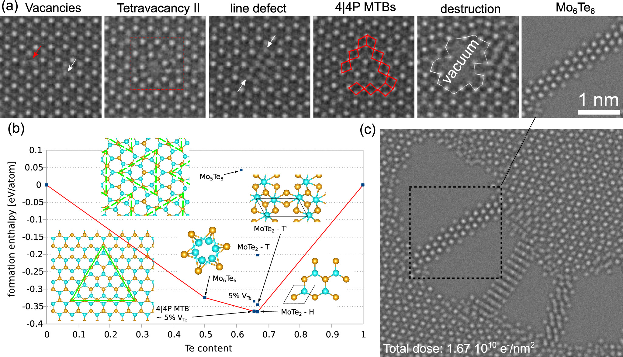
Figure 3. (a) 80 kV HRTEM image sequence illustrating the structure evolution from point defects to Mo6Te6. (b) Convex hull plot of Mo–Te compounds derived from the formation enthalpy per atom. It shows that both the H-MoTe2 phase and Mo6Te6 nanowires are on the convex hull, i.e. they are thermodynamically stable. Therefore, nanowires should form by decreasing the Te content within the single-layer (mediated by the electron beam). (c) Different oriented Mo6Te6 nanowires after a total dose of Øtotal = 1.67 × 10¹⁰ e−/nm2.
Download figure:
Standard image High-resolution imageFirst-principles calculations are employed to analyse the stability of the structures observed in the experiment. For that, the formation enthalpy is calculated. The structures with the lowest formation enthalpy for a given composition are considered thermodynamically stable if the curve connecting these points is convex. This is a well-established construction, referred to as the convex hull, see for example [65]. If structures have negative formation enthalpy but are above the convex hull they are deemed to be thermally unstable (or metastable), and likely decompose into stable phases.
The convex hull of different Mo–Te compounds is shown in figure 3(b). Our calculations predict that Mo6Te6 nanowires and the H-MoTe2 phase are stable. The energy penalty for the formation of a 4|4P MTB in MoTe2 is very low, in agreement with the previous calculations [66], and the MTB is energetically preferable over single Te vacancies (for 4|4P MTB triangular structure, the formation energy difference  per vacancy) meaning that vacancies tend to cluster to form MTBs. However, the proposed MTB network by Junqiu Zhang et al [67] is found to be metastable, as evident from figure 3(b).
After the agglomeration of defects in the hexagonal lattice structure of MoTe2, crystalline nanowires with the formula Mo6Te6 can form (see figure 3(c)). In figure 4(a), the structure model of the found nanowires is displayed. To verify the structure, orientation, and composition of the experimentally acquired nanowires, image simulations based on the structure models are performed using the abTEM API (see figure 4(b)). The details of image simulation with abTEM are given in SI. Line scans taken between the red and blue arrows of the experimental and simulated images are plotted and overlaid in figure 4(c). It is evident from the intensity plot that the experimental image agrees well with the simulated image.

Figure 4. (a) Structure model of a nanowire in side-view. Orange-coloured atoms represent Te and turquois Mo atoms. The side view shows the planar view on the chain and the cross-section view along the nanowire. An experimental and simulated image in (b) illustrates the atom columns viewed along [110] direction. Atom columns in the simulation are marked: yellow (Te); yellow red framed (Te/Mo/Te); and turquoise blue framed (Mo/Mo). Line scans comparing the experiment and simulation of the areas marked by red and blue arrows, respectively, in (b) are shown in (c). (d) Total density of states for pristine system (blue) and system exhibiting a Te vacancy (red).
Download figure:
Standard image High-resolution imageIn addition, our experiments have shown that emerging nanowires are extremely radiation resistant and insensitive to oxidation. Figure 2(c) summarizes the calculated cross section for sputtering a Te atom from Mo6Te6 in the red curves (bold; static case, dashed; Maxwell–Boltzmann (T20°C)). Our DFT calculation estimates Td = 4.90 eV required for displacing a Te atom from a pristine Mo6Te6 nanowire. By taking lattice vibrations into account, the corresponding knock-on threshold is 170 kV. Consequently, no elastic damage is expected in the acceleration voltage range of 40–80 kV. In a second set of simulations, we assessed the required energy to oxidize pristine Mo6Te6 resulting in

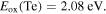
The value of 2.08 eV proves that the pristine nanowire is predicted to be oxidation insensitive, as observed in the experiments. On the contrary, the required energy to oxidize an existing single Te vacancy site is predicted to be

indicating that spontaneous oxidation of a VTe is energetically favorable. Since the properties of a one-dimensional structure should be extremely sensitive to defects, due to the confinement in two-dimensions, and defects can easily appear in low-dimensional materials due to effects of the environment, it appears interesting to access the electronic structure of the nanowires with vacancies. Therefore, the total density of states (DOS) was calculated for the pristine and the defective structure. Figure 4(d) shows the total DOS of pristine (blue) and defect-associated (red) Mo6Te6 nanowires. While pristine MoTe2 with the 4d2 configuration of Mo atoms is a semiconducting material, our calculations predict a metallic character for Mo6Te6. Furthermore, the depicted DOS for the defect-associated case in figure 4(d) shows that the metallic character should be preserved.
3.2. Graphene encapsulation
Although defect creation is a promising way to tailor the properties of a single-layer, we want to demonstrate a route to prevent radiation damage in H-MoTe2, allowing structural analysis even under high electron doses. Figure 5(a) shows a structure model of a vertical heterostructure of G/MoTe2/G in which a single-layer MoTe2 is enclosed between two graphene (G) sheets. Samples were prepared via subsequent transfer of the mechanically exfoliated layers onto a Quantifoil grid, shown in (b). From the experiments we conducted with the G/MoTe2/G structures, it became clear that this type of protection for MoTe2 is an almost indestructible structure for analysis at 40–80 kV voltages. The G/MoTe2/G sample, however, showed dramatically different behaviours, and the vacancy concentration remained unchanged after the electron dose, which completely destroyed the freestanding target. In this context, estimated damage cross-sections of ∼0.006 b and ∼0.005b were determined for a G/MoTe2/G sample at 80 kV and 60 kV, respectively, see inset in figure 2(c).

Figure 5. Electron-driven solid-to-solid transformation of graphene-encapsulated single-layer H-MoTe2. (a) Structure models illustrating the formation of Mo6Te6 nanowires via degradation of H-MoTe2 through holes in one graphene layer. (b) 80 kV Cc/Cs-corrected HRTEM image of the encapsulated H-MoTe2. As inset, the FFT of the layer system and the corresponding reflections of the two encapsulating graphene layers (green and blue) and the H-MoTe2 (red) are shown. (c) Colour-coded map showing bilayer (bi-)graphene in green and graphene encapsulated MoTe2 (G/ MoTe2/G) regions in blue. Red arrows mark a Mo6Te6 NW formed between the graphene layers, enlarged beside (framed in blue).
Download figure:
Standard image High-resolution imageHowever, a sufficiently high dose rate can lead to defects in one (or both) graphene layers of the sample, such that the protective effect of the graphene sandwich is locally abolished. Thus, tellurium and molybdenum atoms can escape the graphene encapsulation [68]. This enables the Mo and Te atoms to leave the graphene pocket so that, subsequently, the formation of NWs encapsulated in between (bi-) graphene is feasible, see figure 5(c). To demonstrate the validity of the protective ability of intact graphene-encapsulation, graphene-encapsulated single-layer H-MoTe2 was annealed to 850 °C in a vacuum. No significant changes in the freestanding H-MoTe2 layer were observed (heating holder, Model 652-Ta) in contrast to emerging changes in the annealing experiments in freestanding H-MoTe2 of lower temperature, which is elaborated in the following.
3.3. Temperature-driven structure evolution of pristine H-MoTe2
Various crystals were transferred onto a micro-electro-mechanical system to investigate the temperature-induced structure evolution of H-MoTe2. We begin our discussion by briefly reviewing the results obtained on crystals with the number of layers (L) between 5 and 20. Despite the use of the dedicated MEMS chips, in which the freestanding flakes are annealed locally, two edge effects occurred. (i) Structural changes mainly formed in areas contacted by the silicon nitride Si3N4 of the heating coil. (ii) Structural changes occur initially at freestanding flake edges. The latter indicates a temperature gradient originating from Si3N4 and a high sensitivity of the flake edges to temperature-driven changes. With the help of EDX and HRTEM at 80 kV, the observed structural changes were analysed in detail, see SI. While the 2D structure H-MoTe2 naturally has twice as much Te as Mo, a 1:1 ratio was detected in EDX after the pristine crystals were annealed. Especially by conducting HRTEM experiments, the changes in the stoichiometry of the material composition could be investigated at the atomic scale and specified as Mo6Te6 nanowires. These have the same structure as previously obtained by electron irradiation. Here, the critical temperature for the phase transformation in few-layer MoTe2 in the range of 550 °C–600 °C was measured. A more detailed study on the structural changes in few-layer H-MoTe2 crystals is provided in the Supporting Information.
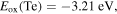
As the number of layers decreased, a reduction in the phase transformation temperature was also observed. For the extreme case of a single-layer, phase transitions have occurred already at 550 °C. Figure 6(a) shows a single-layer H-MoTe2 image just before the abrupt transformation into nanowires. The area used for detail transformation evolution is marked in red, and several atoms are highlighted in solid orange (Te2) and solid turquoise (Mo) to specify the different atomic columns. The area was determined to be 29.6 nm2, corresponding to 548 Te and 274 Mo atoms in a pristine hexagonal single-layer. The number of atoms in the red-framed area was manually counted and resulting in 520 Te and 282 Mo atoms, which corresponds to a Te deficiency of 8.5%.
Figure 6. 80 kV HRTEM images of a freestanding single-layer H-MoTe2 area. From (a)–(b), the single-layer shrivels and forms 1D nanowires at 550 °C. For better visibility, the area of interest is marked in red and several molybdenum columns are marked in turquoise and tellurium columns in orange, representing two tellurium atoms in-column. MTBs are marked by green dotted lines, and dotted red rings highlight symmetric connections of the MTBs. Further, red arrows indicate formed nanowires in which the atom labels as in figure 4(b) are used. (c) Transformed single-layer, showing polymorphic carbon and a molybdenum (Mo) cluster is highlighted in turquoise. (d) Sample annealing to 1000 °C for 15 min. A Mo crystal is labelled in turquoise and a temperature-induced graphene layer is shown. Scale bars represent 1 nm.
Download figure:
Standard image High-resolution image
This single-layer also exhibits a high concentration of triangular-shaped 4/4P MTBs (green dotted lines), connected by symmetric centres marked by red dashed rings. These symmetric centres have one Te2 atomic column located in the middle of a Mo triangle. Showing a high agreement with the published new polymorph v1H-Mo5Te8 structure [67]. In our example, however, the superior structure is not symmetric over a larger distance since the triangular MTB structures are of different sizes. From (a) to (b), the single-layer partially collapses and forms Mo6Te6 nanowires, marked by red arrows  To ensure general validity, the Te deficiency was determined on a second sample by the aforementioned paradigm resulting in a Te deficiency of 9.5%. Only short nanowires were observed in all samples analysed in the single-layer case. We assume that the formation of short nanowires can be attributed to the fast transformation process. It is possibly stimulated by the interplay of the electron beam with the annealed single-layer exhibiting the high Te deficiency, enabling it to overcome the energy barrier to form the energetically stable nanowires (see convex hull in figure 3(b)).
Having shown that the phase transformation in single-layer H-MoTe2 takes place at about 550 °C ± 22 °C, we move on to study whether the Mo6Te6 nanowires are stable at higher temperatures and how the discrepancy between our transition temperature (550 °C) and that reported by Hui Zhu et al 2017 (500 °C) can be explained. Therefore, we analysed the stability of the in figure 6(b) shown nanowire structure. Here, we want to point out that polymorphic carbon can be appreciated, covering the Mo6Te6 network after phase transition at 550 °C, as shown in figure 6(c). As explained in the previous sections, the stability of a single-layer of H-MoTe2 can be significantly enhanced against electron irradiation by encapsulating it with graphene. We therefore assume that carbon contamination on the surface of the single-layer can act as a protecting layer. Thus, this protection effect can explain the differences in the transition temperatures for the solid-to-solid transformation in our experiments, which is 550 °C for the single-layer case, compared to the reported temperature in literature, which is 500 °C reported by Hui Zhu et al 2017.
It is obvious that if more Te atoms are removed from the sample, the Mo concentration will continue to increase until Mo crystals are formed. Even at temperatures as low as 550 °C, we were able to image crystal seeds with a cubic crystal structure, see the turquoise marked region in figure 6(c). It cannot be ruled out that residual Te atoms are still present in the structure, but structural analyses have shown that these seeds can be attributed to Mo crystals. Additional analyses of the crystals shown are attached in the SI. The theory that Mo crystals form was further supported by the fact that we annealed the sample to a higher temperature and performed EDX on the crystals that formed. Therefore, the structure was annealed to 1000 °C for 15 min. Subsequently, pure Mo clusters formed, which no longer have any Te residues, as shown in figure 6(d). The EDX analysis of the Mo clusters is presented in SI. In addition, previously performed annealing experiments with amorphous carbon showed that graphene can be formed under such conditions [69, 70]. In particular, in our experiments we recognized that hydrocarbon contamination on the sample surface, illustrated in figure 6(c), could form polymorphic carbon films, shown in figure 6(d). In addition, this could have been favored by the catalytic effect of the Mo-metal crystals [70]. An exact phase transformation temperature for the transformation of Mo6Te6 to pure Mo crystals could not be worked out. However, with our annealing study in combination with HRTEM, we were able to show that pure ultrathin Mo crystals form from Mo6Te6 nanowires as soon as further Te atoms are released from the structure, at temperatures higher than 550 °C, while graphene is grown.
Eventually, we would like to mention that annealing at 250 °C ± 10 °C of 2H-MoTe2 in an ambient atmosphere leads to oxidation of the material (see Supporting Information), emphasizing again the necessity of vacuum conditions for annealing experiments of two-dimensional materials.
4. Conclusion
The presented in situ Cc/Cs-corrected HRTEM experiments provided insights into annealing- and electron-beam-induced structure transformations of freestanding single-layer H-MoTe2. We show that irradiation with impinging electrons makes it possible to trigger the growth of Mo6Te6 nanowires embedded in the host system after undergoing different degradation steps such as point-, line- and extended defect formation. The process can be controlled by the size of the exposed sample area and the total applied electron dose. In this context, an extensive study of the defect formation in single-layer H-MoTe2 was carried out, which was evaluated with the help of a convolutional neural network and, thus, led to results on damage cross-section in this material for the first time. We have shown that the damage cross sections are of the same order of magnitude, below 0.5b, at electron energies between 40 keV and 80 keV, which is also significantly lower than previously published values for other evaluated TMDs. Therefore, electron irradiation mitigated transformations in single-layer H-MoTe2 can be better monitored and controlled compared to other Mo-based TMDs.
Another route to transform single-layer H-MoTe2 into Mo6Te6 was proven to be in situ annealing in a vacuum of the order of 10−7 mbar with a measured transition temperature of about 550 °C. Here, a Te deficiency of 8%–10% was found to be critical to trigger the phase transformation into Mo6Te6. In addition, our experiments have revealed that temperatures around 1000 degrees Celsius remove even the last Te atoms from the sample, leaving pure Mo crystals behind.
Furthermore, our DFT calculations reveal that the nanowires are energetically stable and are not prone to oxidation. In particular, a metallic character is predicted for a nanowire even with the presence of a single Te vacancy.
In addition, encapsulation of H-MoTe2 with graphene proved to be an excellent protection to suppress all damage mechanisms by electron bombardment or annealing. The phase transformation could thus be suppressed up to approx. 850 °C.
Acknowledgments
We acknowledge the German Research Foundation (DFG) and the Ministry of Science, Research and the Arts (MWK) of the federal state of Baden-Württemberg, Germany, in the frame of the SALVE (Sub Angström Low-Voltage Electron Microscopy) project (KA1295/21-1) and the DFG in the frame of the project 471707562. MKK acknowledges funding from the Deutsche Forschungsgemeinschaft (DFG) within the project DFG: KI 2546/1-1. We acknowledge funding from the European Union's Horizon 2020 research and innovation programs under grant agreement No 881603 (GrapheneCore3). AVK further acknowledges DFG for the support through Project KR 4866/8-1 and the collaborative research center 'Chemistry of Synthetic 2D Materials' SFB-1415-417590517. The authors also thank the HZDR Computing Center, HLRS, Stuttgart, Germany, and TU Dresden Cluster 'Taurus' for generous grants of CPU time.
Data availability statement
The data cannot be made publicly available upon publication because they are not available in a format that is sufficiently accessible or reusable by other researchers. The data that support the findings of this study are available upon reasonable request from the authors.
Supplementary data (3 MB PDF)