
Abstract
Probabilistic (p-) computing is a physics-based approach to addressing computational problems which are difficult to solve by conventional von Neumann computers. A key requirement for p-computing is the realization of fast, compact, and energy-efficient probabilistic bits. Stochastic magnetic tunnel junctions (MTJs) with low energy barriers, where the relative dwell time in each state is controlled by current, have been proposed as a candidate to implement p-bits. This approach presents challenges due to the need for precise control of a small energy barrier across large numbers of MTJs, and due to the need for an analog control signal. Here we demonstrate an alternative p-bit design based on perpendicular MTJs that uses the voltage-controlled magnetic anisotropy (VCMA) effect to create the random state of a p-bit on demand. The MTJs are stable (i.e. have large energy barriers) in the absence of voltage, and VCMA-induced dynamics are used to generate random numbers in less than 10 ns/bit. We then show a compact method of implementing p-bits by using VC-MTJs without a bias current. As a demonstration of the feasibility of the proposed p-bits and high quality of the generated random numbers, we solve up to 40 bit integer factorization problems using experimental bit-streams generated by VC-MTJs. Our proposal can impact the development of p-computers, both by supporting a fully spintronic implementation of a p-bit, and alternatively, by enabling true random number generation at low cost for ultralow-power and compact p-computers implemented in complementary metal-oxide semiconductor chips.
Export citation and abstract BibTeX RIS

Original content from this work may be used under the terms of the Creative Commons Attribution 4.0 licence. Any further distribution of this work must maintain attribution to the author(s) and the title of the work, journal citation and DOI.
1. Introduction
Unconventional physics-based computing technologies are being widely studied, due to the limitations of existing solutions based on the von Neumann architecture in solving computationally hard problems [1]. Two examples of such problems are maximum satisfiability (MAX-SAT) and integer factorization, which have important applications in optimization and cryptography, respectively [2, 3]. To face larger instances of those problems, unconventional computing architectures are urgently needed.
Probabilistic computing is a promising pathway to addressing this challenge [1, 4–12], where a computational problem is mapped onto a network of probabilistic bits, or p-bits [10, 11, 13–16]. A simple description of p-bit dynamics can be mathematically represented as

where k is the current iteration,  represents a random number uniformly distributed between −1 and +1,
  is the sign function which gives an output of either −1 or +1 depending on the input polarity, and
  is the input to the ith p-bit. Depending on the input, the output
  will have a tunable probability of being either −1 or +1. With these rules, probabilistic computing can be exploited to solve problems that can be mapped to quadratic energy models as

where  define the interaction between the ith and the jth p-bit,
  is the local bias to the ith p-bit, and
  is a global scaling factor which can be regarded as an inverse 'pseudo-temperature' [5, 6, 13]. Thus, the input to each p-bit can be obtained by

Computational problems can then be solved through probabilistic computing, by programming the energy model such that the solution corresponds to the lowest-energy state of the network of p-bits.
One of the most important requirements for realizing probabilistic computing is the resource-efficient and scalable physical implementation of p-bits. Magnetic tunnel junctions (MTJs) have been proposed for the implementation of p-bits due to their natural bistability, physical randomness (i.e. stochasticity), low power consumption and compatibility with complementary metal-oxide semiconductor (CMOS) manufacturing. Previously, MTJ-based p-bit designs mainly exploited MTJs with a low energy barrier [1, 4, 14, 17–20], where the randomness arises from the thermal fluctuation of the free layer magnetization, and the probability of finding the bit in each state is tuned by a field or a current through either spin transfer torque (STT) or spin–orbit torque (SOT). Such designs, although well demonstrated in probabilistic computing applications, still have essential limitations: (i) the data retention time (i.e. dwell time) is determined by the energy barrier,  Solving large optimization problems requires high random bit generation rates, which necessitates small
  and—due to the role of demagnetization on the stochastic dynamics of nanoscale magnets—necessitates the use of in-plane MTJs to achieve bit rates of 10 ns or less [21–23]. Since the mainstream MTJs used in MRAM applications today have a perpendicular (out of plane) structure, this requires the addition of separate non-standard MTJ deposition steps to the manufacturing process. (ii) Additionally, it is difficult to fabricate a chip with a tight statistical distribution around a small energy barrier for all devices, further limiting the sampling rate and the number of p-bits achievable on a chip. Materials with small saturation magnetization, such as dilute magnetic semiconductors, have been proposed as a potential solution to the problem of device-to-device variation [24]. However, realizing this potential requires large room-temperature tunneling magnetoresistance in these material systems, which has not been experimentally realized to date [25, 26]. (iii) A feedback loop is needed for each MTJ to adjust the voltage or current, such that the output has the correct probability. This increases the area overhead and makes the circuit less scalable.
Here, we address these issues by proposing a design of p-bits implemented with stable voltage-controlled perpendicular MTJs [27–29], where the voltage-controlled magnetic anisotropy (VCMA) effect [30, 31] is used to dynamically generate true random numbers [32, 33]. This approach offers several advantages: it can be applied to industry-standard perpendicular MTJs and allows the p-bits to be updated with a high speed and on-demand, comparable or faster than p-bits based on superparamagnetic in-plane MTJs. Furthermore, since it does not rely on the precise engineering of a small energy barrier, it can be scaled to a larger number of MTJs with less difficulty. We describe a new way of implementing p-bits using only unbiased MTJs, i.e. MTJs that generate random bit-streams with 50% probability. Therefore, the input to the MTJs does not need to be fine-tuned and the need for analog feedback loops is eliminated, making the circuit more scalable. Lastly, VCMA-based p-bits, owing to their electric-field-based principle [30, 34–58], consume much less energy compared to p-bits tuned via STT or SOT. This provides an ultralow-power solution for realizing probabilistic circuits.
In the next sections, we demonstrate how to use such VCMA-controlled MTJ devices for probabilistic computing applications. We start by showing the generation of true random bit-streams with nano-second voltage pulses, exploiting MTJ stacks with a high VCMA coefficient. The randomness is verified by the National Institute of Standards and Technology Statistical Test Suite (NIST STS) [59]. This is followed by the implementation of p-bits using a series of MTJs at 50% probability. Finally, utilizing these random bits, we implement an invertible multiplier and demonstrate its ability to solve integer factorization problems successfully.
2. Experimental methods
2.1. Device Fabrication
The MTJ film stacks were sputter deposited in an ultrahigh vacuum (UHV) physical vapor deposition (PVD) system (Canon ANELVA HC7100), annealed at wafer level for 30 min at 400 °C, and then fabricated into circular pillars with diameters of 70 nm using electron beam lithography. The MgO layers were deposited by radio-frequency (RF) sputtering, while metallic layers were deposited by DC sputtering.
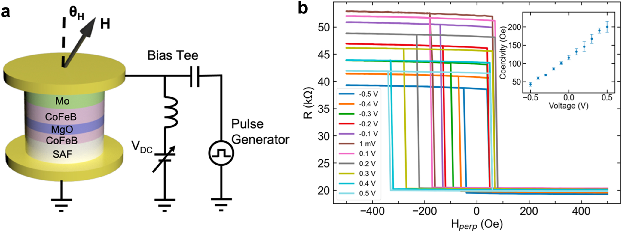
The structure of the MTJs used in this work is shown in figure 1(a). The MTJ stack consists of bottom electrode/pinning layer (which includes a Co/Pt-based synthetic antiferromagnetic, SAF, multilayer)/Co20Fe60B20 (0.8)/MgO (∼1.5)/Co17.5Fe52.5B30 (1.6)/Mo (5)/top electrode. The use of a Mo capping layer, together with the appropriately designed CoFeB composition in the free layer, provide a large VCMA coefficient while preserving a high tunneling magnetoresistance (TMR) ratio and annealing stability up to 400 °C, as previously reported [58]. The film was patterned into circular pillars with diameters of 70 nm.

Figure 1. Device structure. (a) Diagram illustrating the structure of the magnetic tunnel junctions and the measurement circuit used in this study. Voltage pulses are applied by a fast pulse generator to the device via the RF port of a bias tee and the device resistance is measured by a sourcemeter using the DC port. An external magnetic field (H) is applied at an angle θH from the film normal to compensate for the non-zero stray field acting on the free layer. (b) Resistance as a function of the applied out-of-plane magnetic field under different DC bias voltages. The inset shows the coercivity as a function of applied voltage.
Download figure:
Standard image High-resolution image2.2. Electrical measurements
Characterization of the MTJs was performed on a probe station while applying an external magnetic field by a projected field electromagnet, as shown in figure 1(a). Electrical measurements were performed using RF probes with a ground-signal (GS) configuration. The voltage pulses for reconfiguring the MTJ magnetic anisotropy were generated by a Tektronix pulse generator (PSPL10070A), and the electrical resistance was measured by a sourcemeter (Keithley 2401) using a bias tee.
3. Results and discussion
3.1. Device Structure
The resistance as a function of perpendicular magnetic field under different bias voltages for a representative device is shown in figure 1(b). As the magnetization of the bottom CoFeB layer is coupled to the SAF pining layer, only the magnetization of the top CoFeB can be changed by the applied field. These two layers are denoted as the free and fixed layers, respectively. The low and high resistance levels correspond to the parallel (P) and anti-parallel (AP) orientations of these two layers. At the near-zero bias case (shown as 1 mV in figure 1(b)), the TMR ratio is approximately 170%, defined as  Importantly, the change in the coercivity under different bias voltages confirms the presence of the VCMA effect. The VCMA coefficient for the stack used in this work was measured to be ∼130 fJ Vm−1. Note also that the device has a sizeable coercive field of ∼120 Oe in the absence of voltage, indicating that it is not a stochastic MTJ in the absence of voltage.
3.2. VCMA-induced generation of true random numbers
Using the VCMA effect, it is possible to dynamically generate random numbers, in a fast and energy-efficient manner, from a perpendicular MTJ that is stable in the absence of voltage at room temperature. To do so, a short voltage pulse is applied to the MTJ with a polarity that reduces the perpendicular anisotropy of the free layer due to VCMA. If the magnitude of this voltage exceeds a threshold value, the magnetization of the free layer will relax in an in-plane direction after damped precession within a few nano-seconds [34, 45–58]. If the voltage pulse is removed at this point, the anisotropy is restored to the original perpendicular axis, and the magnetization aligns to one of the two perpendicular states with equal probability. Therefore, the device can perform as a true random number generator (TRNG) with 50% probability of generating P or AP states. This process is illustrated in figure 2(a).

Figure 2. Dynamic generation of true random numbers. (a) Principle of dynamically generating true random number by VCMA. When the voltage pulse is applied, the perpendicular anisotropy is temporarily eliminated, and the free layer becomes in-plane after damped precession. After the voltage is removed, the device will go to the P or AP state with equal probability. (b) Time-domain measurement result of the device resistance after a train of identical 10 ns voltage pulses.
Download figure:
Standard image High-resolution imageThe circuit for the generation and measurement of the random numbers is shown in figure 1(a). Voltage pulses were applied to the MTJ through the RF port of the bias tee by a pulse generator, and the resistance of the MTJ was measured after each pulse using the DC port. During the application of voltage pulses, a fixed magnetic field was applied at an angle of θH from the film normal in order to both compensate for the offset field and define an in-plane axis for the precession of the magnetic moment of the free layer. To generate random numbers, voltage pulses of 2.2 V were applied with a pulse width of 10 ns. It is worth noting that due to the reflection resulting from the impendence mismatch between the MTJ and the transmission line, the real voltage experienced by the MTJ is approximately twice the output value from the pulse generator. The amplitudes of the voltage pulses discussed in this paper correspond to the real voltage on the device. An example of the measured resistance after a sequence of voltage pulses is illustrated in figure 2(b), which shows a random binary behavior.
The quality of the bit-streams was verified by using the National Institute of Standards and Technology Statistical Test Suite (NIST STS) [59]. Before testing, two layers of XOR gates were used, as indicated in figure 3(a), to further randomize the bit-streams [18]. The test results are shown in figure 3(b). The output bit-stream successfully passed through all the NIST tests.

Figure 3. VCMA-based TRNG evaluation. (a) XOR gates are used to improve the quality of the bit-streams before the NIST test. (b) NIST test result for the output bit-stream after the XOR gates. All tests are passed by the VCMA-generated random bit-streams.
Download figure:
Standard image High-resolution imageNote that, in an on-chip implementation, a wide range of fast readout circuits can be used for sensing the resistance of the MTJ after each 10 ns voltage pulse. For example, a prior study has investigated a circuit design for high-throughput VCMA-based RNGs based on the 45 nm CMOS node [32]. A sensing time of ∼1 ns was demonstrated, which is quite small compared to the duration of the VCMA pulse. Thus, the bit-rate from a single MTJ in this approach can indeed be close to 100 Mbps when integrated with an appropriate readout circuit.
3.3. Implementation of p-bits
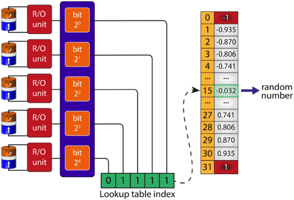
As discussed previously, existing p-bit designs using MTJs are mainly based on free layers with low energy barriers, where the probability profile of the p-bit is tuned by analog signals. This is a drawback for scalability purposes, both due to the need for accurate control of individual analog signals across a large number of p-bits with different nonlinear transfer curves, and due to the difficulty of realizing arrays of p-bits with tight statistical control of a small energy barrier. Here, we propose a new design of p-bits using only unbiased voltage-controlled MTJs that generate a 50% bit-stream. In our design, each p-bit consists of a series of n MTJs. When a p-bit is activated, voltage pulses are applied to all the n MTJs and generate an n-bit binary number, b, which can in turn be used to divide the range of numbers (−1, 1) into  evenly spaced segments. Therefore, b can be mapped to a decimal number within (−1, 1) by
  An example is illustrated in figure 4, where a p-bit consists of five MTJs (n = 5). The five MTJs are shown to provide a binary number of 01111, which is 15 in decimal and thus can be mapped to
  This approach can be used to implement, in hardware, the function
  in equation (1). The key advantage of this design is that the bias term (i.e. the hyperbolic tangent function in equation (1)) is calculated in conventional digital logic instead of analog signals applied to each MTJ, making the circuit less complicated and more scalable. The accuracy is therefore determined by the number of MTJs used for each p-bit (rather than the accuracy of an analog bias current), so that using more MTJs in each p-bit provides better accuracy. Note, however, that this comes at the expense of a larger memory requirement for the overall p-computing circuit, since the tanh curve needs to be implemented in a look-up table (LUT).

Figure 4. Implementation of p-bits using VCMA-controlled MTJs. Implementation of a p-bit with a series of five MTJs. The binary output from the MTJs, measured using the readout (R/O) units, is mapped to a decimal number within the range (−1, 1), which in turn can be used to implement the p-bit based on equation (1).
Download figure:
Standard image High-resolution imageIt is worth noting that, a number of ideas utilizing the VCMA effect to implement p-bits have been previously proposed [60–62]. In these works, a voltage pulse is applied to generate the free layer precession, with a pulse duration that is tuned to half of the precession period. The switching probability is then tuned by another torque from STT [60, 61] or SOT [62], to implement the hyperbolic tangent bias term. In these designs, both the pulse width and the pulse amplitude need to be accurately controlled to ensure a reliable output, which necessitates a dedicated control circuit and a calibration process to account for device-to-device variations.
3.4. Integer factorization using VCMA-based invertible logic gates
Next, using the proposed p-bit design and experimentally measured random bit-streams from voltage-controlled MTJs, we solve integer factorization problems as an example of probabilistic computing. A key property of probabilistic computing, which distinguishes it from existing digital computing circuits, is that it can be used to build invertible logic gates [13], similar to memcomputing [63, 64]. Conventional logic gates can only function in one direction. When their inputs are given, the gate will provide the corresponding output according to a truth table. For invertible logic gates, however, when the output of the logic gate is clamped (i.e. fixed), the inputs explore with higher probability the states allowed by the gate's truth table. In other words, the inputs will fluctuate among all possible states that will be consistent with the given output.
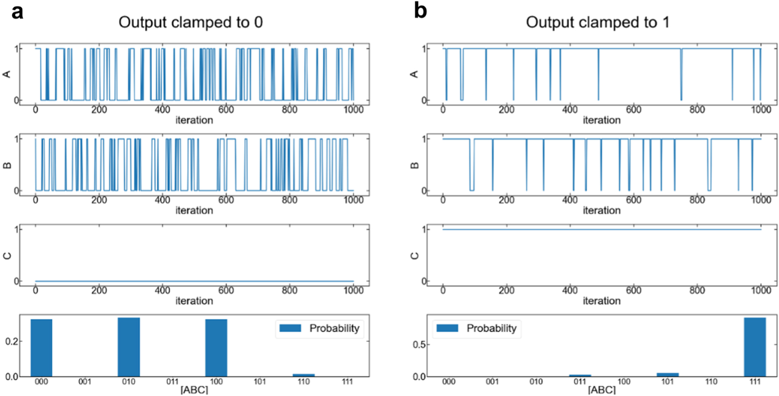
Such an invertible gate can be realized by designing the appropriate J matrix and h vector in equation (2). An example of an invertible AND gate is illustrated in figure 5. Details on the derivation of the corresponding J matrix and h vector are shown in Supplementary Note 1. Here, A and B represent the two p-bits for the input and C represents the output. Each p-bit is realized in software using experimentally measured bit-streams from a 70 nm voltage-controlled MTJ, according to the method shown in figure 4. The top three plots in figures 5(a) and (b) show the traces of how the three p-bits evolve with time, when the output is clamped to 0 and 1, respectively. The bottom figures summarize the probability of the occurrence for each combination, confirming the functionality of the invertible AND gate.

Figure 5. Invertible AND gate. The evolution of three p-bits and the probability of each state combination, when (a) the output p-bit C is clamped to 0, and (b) the output p-bit C is clamped to 1. The results are consistent with the truth table of an invertible AND gate.
Download figure:
Standard image High-resolution imageIn order to construct the circuit for integer factorization, we repeated the process used for the AND gate to also demonstrate an invertible full adder and half adder. These three circuit elements were then combined to construct a standard 4 × 4 bit multiplier, as illustrated in figure 6(a). If all the inputs are given, the circuit acts as a conventional multiplier. However, due to its invertible nature, if the output bits are clamped, the system will also act as a factorizer. Figure 6(b) shows the distribution of states when attempting to factor the semi-prime number 91. Note that 91 can be factorized into both 7 × 13 and 13 × 7; therefore, the system will have two energy minima and will descend into one of them. In the case shown in figure 6(b), the system converged to the energy minimum of 7 × 13.
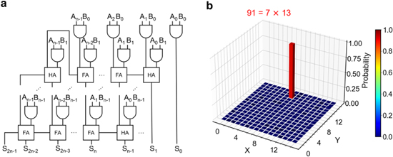
Figure 6. Integer factorization using invertible logic gates. (a) Circuit diagram of the invertible multiplier consisting of AND gates, half adders (HAs), and full adders (FAs). (b) Distribution for the probability of the input (X, Y) pair being at different combinations of numbers, when factorizing the semi-prime number 91.
Download figure:
Standard image High-resolution imageIt is worth noting that the factorization problem can also be solved using VCMA-based p-bits by directly designing the appropriate J matrix and h vector (as opposed to breaking the problem down into individual gates and adders). This approach was also implemented and allowed us to solve up to 40-bit factorization problems. The result is shown in figure 7, demonstrating the factorization of the semi-prime number 1,099,467,063,467. The detailed implementation is discussed in Supplementary Notes 2 and 3.

Figure 7. Integer factorization of 1,099,467,063,467. Distribution for the probability of the input (X, Y) pair being at different combinations of numbers, when factorizing the semi-prime number 1,099,467,063,467.
Download figure:
Standard image High-resolution image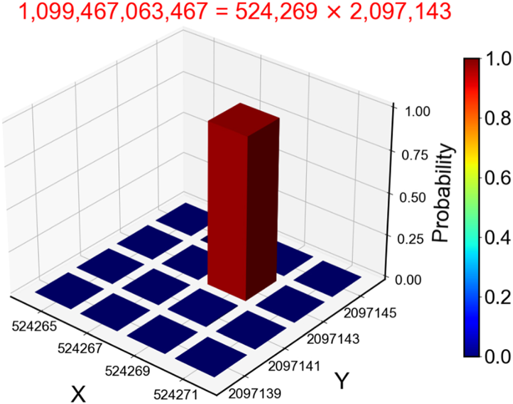
4. Conclusions
In summary, a p-bit based on an array of voltage-controlled MTJs was proposed, and its proof of concept was demonstrated for probabilistic computing applications. The VCMA effect allows for dynamic nano-second true random number generation using voltage pulses applied to a perpendicular MTJ stack. The quality of the randomness was verified by passing the NIST statistical test suite. The proposed p-bit design improves the scalability of probabilistic circuits by eliminating the need for tight control of small energy barriers during manufacturing, eliminating the need for a feedback loop for analog signals, and by using industry-standard perpendicular (rather than in-plane) MTJs. We demonstrated the application of our VCMA-based p-bits in solving integer factorization problems using experimental MTJ-generated bit-stream data. Our results provide a promising direction for using VCMA-controlled MTJs in unconventional computing applications.
Acknowledgments
This work was supported by the U.S. National Science Foundation (NSF) under award numbers 2311296, 1919109, and 2106562. The authors thank Canon ANELVA Corporation for part of the magnetic thin film deposition and characterization. ER and GF acknowledge financial support of the project PRIN 2020LWPKH7 funded by the Italian Ministry of University and Research (MUR), and the PETASPIN association (www.petaspin.com).
Data availability statement
The data that support the findings of this study are available upon reasonable request from the authors.
Competing interests
The authors declare no competing interests.
Supplementary data (0.4 MB PDF)