
Abstract
Molecular thin films, such as self-assembled monolayers (SAMs), offer the possibility of translating the optimised thermophysical and electrical properties of high-Seebeck-coefficient single molecules to scalable device architectures. However, for many scanning probe-based approaches attempting to characterise such SAMs, there remains a significant challenge in recovering single-molecule equivalent values from large-area films due to the intrinsic uncertainty of the probe-sample contact area coupled with film damage caused by contact forces. Here we report a new reproducible non-destructive method for probing the electrical and thermoelectric (TE) properties of small assemblies (10–103) of thiol-terminated molecules arranged within a SAM on a gold surface, and demonstrate the successful and reproducible measurements of the equivalent single-molecule electrical conductivity and Seebeck values. We have used a modified thermal-electric force microscopy approach, which integrates the conductive-probe atomic force microscope, a sample positioned on a temperature-controlled heater, and a probe-sample peak-force feedback that interactively limits the normal force across the molecular junctions. The experimental results are interpreted by density functional theory calculations allowing quantification the electrical quantum transport properties of both single molecules and small clusters of molecules. Significantly, this approach effectively eliminates lateral forces between probe and sample, minimising disruption to the SAM while enabling simultaneous mapping of the SAMs nanomechanical properties, as well as electrical and/or TE response, thereby allowing correlation of the film properties.
Export citation and abstract BibTeX RIS

Original content from this work may be used under the terms of the Creative Commons Attribution 4.0 licence. Any further distribution of this work must maintain attribution to the author(s) and the title of the work, journal citation and DOI.
1. Introduction
The translation of highly promising single-molecule thermoelectric (TE) properties to scalable thin films is of considerable fundamental and practical interest. In TE devices electricity is generated by the Seebeck effect and defined by the Seebeck coefficient,  where
where  is the TE voltage generated in response to a temperature difference
  across the device.
Recent studies of single-molecule and thin-film quantum interference effects have highlighted the fundamental relationships between transport properties, TE performance and molecular structures and signposts new scalable routes to high-Seebeck-coefficient materials [1–8]. However, new measurement techniques are needed to confirm that these single-molecule properties can be translated to scalable molecular energy-conversion devices. These techniques should be capable of mapping, with nanoscale resolution, the electrical and TE properties of delicate, ultra-thin molecular films. Molecular-scale thermopower has been measured using a variety of test beds such as scanning tunnelling microscopy, mechanically and electrically controlled break junctions, and atomic force microscopy (AFM) based approaches such as thermal-electric force microscopy (TEFM) [2, 6, 9, 10]. TEFM is a particularly versatile method, which integrates the conductive-probe AFM (C-AFM) with an electrical heater interactively controlling the temperature of the sample. For molecular self-assembled monolayers (SAMs), the TEFM enables the simultaneous measurement of clusters of 10–103 molecules, with controllable normal force [11, 12]. However, the high lateral forces between the probe and the sample in contact AFM modes can cause damage to the molecular layers. Here we show a route to overcoming these damaging interactions for molecular TE characterisation by employing a peak force tapping (PFT) feedback approach to control the probe-sample interaction in real-time.
The PFT mode of AFM operation (e.g. Bruker's PeakForce™ Tapping) introduced by Su et al [13] is a high-speed (0.5–4 kHz), small-displacement (20–150 nm) force spectroscopy mode, based on the rapid collection of point-by-point force curves, where the peak probe-sample interaction force of each force curve is used as the topography imaging feedback signal. This enables sub-nN-levels of probe-sample interaction measured directly by the deflection of the cantilever [14, 15]. The precisely controlled maximum normal force and effective elimination of lateral forces during scanning due to tip-surface contact being broken during each cycle, make the PFT mode especially suitable for studying organic systems. In this work, we have combined a TEFM setup with the PFT mode of surface mapping to extract electrical, thermoelectrical and nano-mechanical properties of thiol-terminated SAMs showing that, per molecule, they are directly comparable to true single molecule measurements.
All measurements are performed on molecular layers assembled on template-stripped Au during the contact portion of the force curve cycle. PFT setup offers several advantages [16–19] compared to standard contact mode AFM which operates, typically, in the normal force ranges of 2–10 nN, and where the unavoidable lateral forces in the junction during scanning generally result in rapid destruction of both the SAM and the metallic coating at the apex of the conductive probe tip (see supplementary information figure S1(a)) and, most notably, the SAM structure (figure S1(b)). In addition, PFT mode typically offers better spatial resolution than contact mode for mapping soft materials, due to the inherently smaller contact area between probe and sample at low forces, and allows the simultaneous acquisition of nanomechanical properties, such as local adhesion and elastic modulus, of the sample. In all experiments reported here, we compared the C-AFM and TEFM operating in PFT mode (figure 1(b)) to the same system operating in contact mode (figure 1(a)).

Figure 1. Experimental setup of TEFM in (a) contact mode and (b) PFT mode. In both cases, the temperature of the sample was controlled by a Peltier stage. A function generator combined with a 10× amplifier was used to heat up and cool down the sample. A boron-doped diamond probe (tip radius < 25 nm) with high thermal (∼1000 W m−1 K−1)) and low electrical resistance (∼1 kΩ) was used both as the thermal sink and the voltage sensor. (c) Chemical structure of all molecules measured in this work.
Download figure:
Standard image High-resolution image2. Methods
2.1. Au preparation
The ultra-flat gold was prepared by modifying the template stripped (TS) method of Whitesides and Pinkhassik [20] on mica (Agar scientific). A Si wafer (5 mm × 5 mm) was ultra-sonicated in acetone, methanol and isopropanol in succession and then cleaned with oxygen plasma for 5 min. The cleaned wafer was glued with Epotek 353ND epoxy adhesive to the top surface of a onto the 200 nm gold layer thermally evaporated on a clean Mica substrate to form a Si/Glue/Au/Mica sandwich structure. The epoxy was cured for 40 min at 150 °C. The TS-Au was obtained by peeling off the mica with a knife to expose the ultra-flat Au surface. TS-Au was subsequently checked by AFM in 3–5 random spots; for all substrates prepared, the average roughness of the gold was below 70 pm (in figure S2).
2.2. SAM preparation
SAMs were deposited from 100 μM solutions of the target molecules. Hexanethiol (C6S), Octanethiol (C8S) and dodecanethiol (C12S) solutions were prepared in ethanol (spectroscopy level) whilst Biphenylthiol (BPT) was prepared in toluene (HPLC level). Solvents were deoxygenated for 10 min by nitrogen bubbling. All materials were obtained from Sigma Aldrich and used without further purification. The TS-Au was immersed in the solution, and incubated for 24 h in a nitrogen atmosphere. To eliminate extraneous physisorbed materials, the C6S, C8S and C12S samples were then rinsed with ethanol, and the BPT sample rinsed with toluene followed by ethanol. Samples were subsequently dried with blown nitrogen and incubated in a vacuum oven (10–2 mbar) overnight at 35 °C to ensure solvent evaporation.
2.3. QCM measurement
For each measurement a new Au-QCM crystal (5 mm diameter, f0 = 10 MHz, from Novaetech S.r.l) was washed with acetone, methanol and isopropanol in series, cleaned with oxygen plasma, and incubated in a vacuum oven at 50 °C for solvent evaporation. The resonance frequency of the cleaned QCM was recorded using a commercial monitoring system (Q-1 from OpenQCM). SAMs were deposited on the cleaned crystal used the method detailed and the modified QCM resonance frequency recorded. The difference between these two frequencies is related to the occupation area per molecule Amolecule attached to the electrode surface as described by the Sauerbrey equation below [21]:


where A' is the electrode area, A the crystal area, Δf the frequency change, Mw the molecular weight, NA the Avogadro's number, μ the shear modulus of quartz, ρ the density of quartz, and f0 the initial frequency. Detailed QCM information is listed in table 1.
Table 1. Detailed information on QCM on different SAMs molecules.
| SAM | Δf (Hz) | Occupation area per molecule (Å2) |
|---|---|---|
| C6S | 33.9 | 26.0 |
| C8S | 45.4 | 24.1 |
| C12S | 73.3 | 20.7 |
| BPT | 61.5 | 22.6 |
2.4. AFM workflow
The Multi-Mode 8 AFM (with Nanoscope 5 controller, Bruker) was used for all AFM measurements, with the experimental setup of C-AFM and TEFM explained in detail below. The thermovoltage was extracted in two ways. For contact mode measurements, the '0 current mode' was used. A thermally and electrically conductive probe (doped diamond, CDT-CONTR, NanoAndMore, thermal conductivity ∼400–2000 W (m K)−1, radius of curvature ∼100 nm, force constant 0.5 N m−1) isolated from the probe holder was used both as the top electrode and thermal sink, then engaged in the normal way (force set point at 5 nN). The sample was heated up and cooled down by a Peltier stage (2.4 W, Laird Technologies) controlled by a function generator and a voltage amplifier. The temperature of the sample during measurement was calibrated by a Cu-Ni thermocouple attached to a bare gold, and the temperature of top part of SAMs was calibrated by a KNT probe (KNT-SThM-1AN, Windsor Scientific), which has a similar radius of curvature (∼100 nm) to the conductive probe, but has 45 nm thick palladium resistive thermometer at the end of the probe for temperature sensing (figure S3). The voltage difference between sample and probe was collected by a high-impedance differential pre-amplifier (SR 550, Stanford Research Systems) at zero bias, passed through a low pass noise filter (SR 650 Stanford Research Systems), and the filtered signal was acquired by the Nanoscope controller in real-time (figure 1(a)), the instrumental offset of the measurement was calibrated at ΔT = 0 K. The temperature difference between the bottom gold and top part of SAMs indicates the temperature drop across the molecules ( ).
).
A major challenge of measuring a thermovoltage by PFT in '0 current' mode is that the characteristic time of voltage change is much slower than the PFT frequency due to the capacitance of the probe, which does not allow the signal to be acquired by a lock-in amplifier. For this reason, we used a 'current sensing' mode. Since the current only appears when the probe touches the sample surface, and as I–V converter current input provides the 'virtual ground' thereby drastically reducing influence of the probe and connecting wires capacitance, the response time is sufficiently short and well below the time of contact (typically 0.1–1 ms). A triangular shaped AC electrical bias was applied between tip and sample (−1 to 1 mV) at low frequency (2 Hz) creates a response current, with current–voltage I–V converter with 1 V nA−1 fixed gain and 5 fA/√Hz input noise (SR 556, SRS) used to convert the tip-sample current into the voltage. The averaged current signal 'bursts' at PFT frequency were acquired by the lock-in amplifier (SR830, SRS) with the derivative of Z-motion signal of the AFM stage used as the reference for the lock-in amplifier. The resulting amplitude of time-modulated current at different temperature was acquired by the AFM controller (figure 1(b)) simultaneously with the bias voltage, allowing easy post-processing of the data.
2.5. Nanoscratching
A small area of a deposited SAM was scanned repeatedly in contact mode at high force (30 nN), followed by a larger area scan at low normal force (2 nN). A cleaned 'window' is observable in the small high-force-scanned region where the molecules have been scratched away and the thickness of the SAM can be measured [22–24]. For all samples the SAM thicknesses corresponded to monolayer growth consistent with QCM measurements.
2.6. Theoretical methods
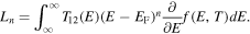
Electronic structure calculations were conducted using the SIESTA [25] implementation of density functional theory (DFT) with the PBE exchange-correlation functional. For the Au atoms a double zeta basis set was used; for other atoms the basis set was double zeta polarised. The mesh cut-off was 200 Rydberg and relaxations were performed to a force tolerance of 0.01 eV Å−1.
Molecular junctions were constructed using two leads with a single molecule or 9 molecules between two gold electrodes. Each lead consisted of five Au (111) layers periodic in the x- and y-directions. The whole structure was periodic in the z-direction (direction of thermal and electrical transport). The distance between the molecule and each lead in the z-direction was determined by separate relaxations of a single molecule with each lead. The junction was then assembled and the molecule was allowed to further relax, resulting in the S atoms lying in the hollows of the Au surface lattice. For junctions of 9 molecules in figure S9, further copies of the molecule in the same configuration were placed at intervals of 5.0 Å in a  pattern [26–29].
For the calculations, the configurations of BPT molecules were taken from a molecular dynamics simulation (figure S5) performed using the DL_POLY classic package, with the OPLS 2005 force field, using DL_FIELD to prepare input files. The sulphur atoms were frozen, mimicking the effect of bonding to a Au surface. The simulation consisted of 1 ps of equilibration at 293 K followed by a 100 ps production run in the microcanonical ensemble, with a timestep of 1 fs. There were 25 BPT molecules in the simulation cell, with periodic boundary conditions, from which the coordinates of 9 molecules were extracted every 20 ps for use in transport calculations.
From the Hamiltonian and overlap matrices of the DFT calculation of the junction, the transmission function  was computed with the transport code GOLLUM [30] using the relation
where  is the (retarded) Green's function of the junction and
  is the imaginary part of the self energy of electrode
  The conductance and Seebeck coefficient as a function of the average temperature
  of the two electrodes are [31, 32]


where
3. Results and discussion
3.1. SAM growth and stability
The SAM-forming molecules, shown in figure 1(c), grown on TS-Au from mica were investigated in this work: saturated wires with different lengths formed from C6S, C8S or C12S, and a conjugated wire formed from BPT. In each case, SAM growth was monitored by a quartz crystal microbalance (QCM), with a gold electrode to determine molecular packing in the film. Assuming 100% surface coverage, a Sauerbrey analysis indicated the occupation area of a single C6S, C8S, C12S and BPT molecule on the Au substrate is 26.0 Å2, 24.1 Å2, 20.7 Å2 and 22.6 Å2 respectively, which is comparable with literature values obtained by reductive desorption [33] and our theoretical calculations (see figure S9). SAM quality was characterised by AFM measurement topographical imaging. For C8S and C12S SAMs, the average roughness of the sample is smaller than 70 pm, which is in the limit of the measurement accuracy of the AFM instrument, indicating the SAMs are arranged in a highly uniform manner. For BPT SAMs, the average roughness was 120 ± 20 pm (figure S7) and is believed to be due to the higher conformational degree of freedom of BPT molecules in SAMs [34, 35]. SAM heights are measured by nano-scratching and are in the expected range corresponding to molecular lengths of 0.7–1.5 nm, indicating that the molecules are 'standing up' on the substrate surface with tilt angles of about 45°–80°; this agrees with QCM result given in table 1. In all cases, the averaged roughness of the sample is smaller than 15% of the SAM thickness, with no obvious pin-holes (>10 nm) or physisorbed clusters.
Microscale temperature uniformity of the Peltier temperature controlled stage was established (figure S11) and the temperature of the sample was calibrated by the temperature of bare template-stripped Au (see methods and figure S12). SAM stability at elevated Peltier stage temperatures was studied by standard PFT-AFM (figure S13); we observed that the SAMs become unstable during scanning above an absolute stage temperature of 50 °C and hence, all measurements reported below are taken in the stage temperature range of 20 °C–45 °C.
3.2. Thermovoltage characterisation
Thermovoltage characterisation was performed on SAMs of C8S and BPT on TS-AU. These two molecules have comparable molecular lengths but, as single molecules, significantly different electrical transport properties. Figure 2 shows the measured thermovoltages where (a), (d) are obtained in contact mode using '0 current mode' measuring the probe potential and (b), (e) in PFT mode using 'current sensing mode' where the current through the tip connected to the I–V converter is measured. The temperature of the system is varied via the application of voltage to the Peltier stage (figures S3, S4 and S12).

Figure 2. TE study of different junctions. (a), (d) TE measurement of C8S and BPT via contact method (detailed data in figure S10). (b), (e) TE measurement of C8S and BPT via PFT method (detailed data in figure S8). (c) Comparison of Seebeck coefficient obtained via contact and PFT method. (f) Distribution of measured Seebeck value for C8S and BPT, dash line is the theory predicted value.
Download figure:
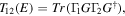
Standard image High-resolution imageFor 0 current mode, the Seebeck coefficient, S, is calculated by the following relation [10]:
where ΔV is the thermovoltage, ΔT the calibrated temperature difference between the sample and probe. The calculated Seebeck coefficients are SC8S = 7.4 ± 3.1 μV K−1, and SBPT = 23.3 ± 7.3 μV K−1. For reference bare Au a Seebeck coefficient was measured to be SProbe Au = 4.0 μV K−1 (figure S14). This result is comparable with other works on similar systems [6, 36, 37]. The positive sign of SC8S and SBPT indicate that transport through the molecules is HOMO dominated in agreement with our calculation. The measured Seebeck of C8S is about 3 times smaller than BPT, which correlates with the larger HOMO-LUMO gap of C8S, and the fact that Fermi-energy, EF lies within in the gap closer to HOMO.
Using the current sensing mode, the relation between current and Seebeck coefficient follows the relation:


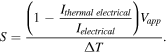
The derivation of this is described in supplementary information (equation (S1)), ΔT is the temperature difference between the probe and sample, Ielectrical is the measured current when ΔT = 0, G is the conductance of the molecules, Vapp is the bias voltage between sample and probe. Using this method, the measured Seebeck coefficients are SC8S = 9.3 ± 3.1 μV K−1 and SBPT = 17.6 ± 5.5 μV K−1, which is within measured uncertainties of the contact AFM approach giving strong indication of the validity of this method (figures 2(c), (f)).
An example of Seebeck mapping is shown in figure S15(b). Two current maps of an C8S sample at the same area with two different temperatures (ΔT = 0 and 14 K, bias voltage = 1 mV) are obtained producing a voltage difference. Figure S15(c) shows the statistics of the thermovoltage from the two current maps used for figure S15(b).
3.3. Electrical conductivity
Conductivity measurement of SAMs was performed using the same experimental setup with the addition of a home-built current pre-amplifier based on AD4000 low-noise op-amp mounted in the Bruker AFM tip holder. Figure 3 shows the electrical conductance information of BPT SAMs by contact mode and PFT mode. The current maps show higher disorder than equivalent measurements on C8S and C12S (figure S16) likely due to the higher surface roughness and conformal degrees of freedom.
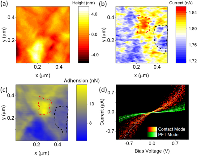
Figure 3. (a)–(c) The topography image (a), current map (bias voltage 500 mV) (b) and adhesion map of BPT SAMs obtained via PFT mode described in this work. (d) IV curve of BPT from contact and PFT mode, similar trend with the work in contact mode giving strong indication of the validity of this method.
Download figure:
Standard image High-resolution imageFigure 3(c) shows the simultaneous mapping of local nanomechanical properties—here the adhesion force between probe and sample—one of the main advantages of PFT mode. The black and red dash line region in figures 3(b) and (c) indicate the positive relationship between tip-surface adhesion force and tunnelling current, which indicate stronger tip-organic coupling enhances the junction tunnelling efficiency. Correlating such information allows us to study the nature of the probe-molecule interaction beyond that enabled by topography alone to identify the condition of the interface. The I–V curve of BPT from contact mode and PFT mode is shown in figure 3(d), (statistics in figures S15 and S16).
For conductance mapping, we observe that current intensity from contact mode (figure S17) is about 5 times higher than that from the PFT mode. The electrode (probe-substrate) separation is predicted to decrease by ∼0.5 nm between PFT and contact modes (at applied normal forces of 0.2 and 5 nN respectively), as such the increased conductance is believed to arise from a change in the molecular tilt angle—relative to the electrode—due to the decreasing electrode separation at increasing normal force [38] and is in broad agreement with predictions theoretical predictions (figure S18 and table S1) over a corresponding change in electrode separations. The predicted range of molecular angles due to increasing force remain consistent with the range measured by QCM above. It is worth noting, that for Seebeck measurements using PFT mode, since we are considering the ratio between the TE current and the electrical current instead, the current intensity drop need not be considered.
The number of molecular junctions formed between probe and sample is estimated from the tip-sample contact radius and QCM derived area per molecule (section 2.3). The tip-sample contact radius was estimated via equation [39]:

where, r is the contact radius, F is the loading force from probe to sample, R is the radius of the probe, v1
and v2
are the Poisson ratio of the material, E1 and E2 the Young's Modulus for probe (∼100 GPa) and SAMs (∼0.5–1 GPa for alkyl thiolates, 9 GPa for BPT) [40, 41], respectively. A summary of molecular occupation area, contact radius, contact area and number of molecular junctions is given table S2. The single molecular conductance of BPT, C6S, C8S and C12S is calculated to be 
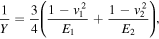
 correspondingly. The decay coefficient for alkyl-thiolate, β, is found to be 9 ± 1.2 nm−1 for contact mode and 11.8 ± 1.8 nm−1 (figure 4(a)) for PFT mode via equation:

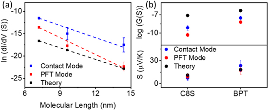
Figure 4. (a) Semilog plot of tunnelling current decay versus molecular length of alkyl thiolates (C6S, C8S and C12S) measured by contact mode, PFT mode (measured value), and theoretical prediction (detailed distributions in figures S6, S19 and S20). (b) Comparison of conductance and Seebeck coefficient for C8S and BPT via contact mode, PFT mode (calibrated to single molecular equivalence) and theoretical prediction.
Download figure:
Standard image High-resolution imageBoth values are in the expected range (7–12 nm−1) from other experimental work and theoretical calculations [42–45].
3.4. Transport calculations
To understand theoretically the transport properties of BPT and C8S, we use the SIESTA DFT package, and the Green's function transport code Gollum. The structures of idealised SAMs of BPT and C8S are shown in figure 5(a). The Seebeck coefficient and electrical conductance per molecule of clusters of 9 molecules are found to be very similar to single molecule junctions (see figure S6). For Fermi energies in the vicinity of the DFT predicted Fermi energy  the transport of both BPT and C8S is HOMO dominated with a positive Seebeck coefficient, in agreement with the experimental results of figure 2. Averaging G and S over a range of Fermi energies 0.025 eV on both sides of
  eV gives
  = 18.2 μV K−1 for BPT and 11.2 μV K−1 for C8S (figure 4(b)), in good agreement with the experimental values. The smaller HOMO-LUMO gap of BPT (3.4 eV) compared to C8S (5.3 eV) means that the slope of the transmission function T(E) close to the HOMO is steeper, hence the larger value of S, as S is roughly proportional to
  (figure S21). The averaged conductances are
 for BPT, and
  for C8S (figure 4(b)).
Figure 5. (a) Idealised SAM structures of BPT and C8S with Au leads. (b) Transmission function and (c) thermopower of single molecule junctions. (d) Range of thermopower and conductance values using fermi energy window of 0.05 eV centred on  eV. (e) Transmission function for series of alkylthiolates C6S, C8S, C10S, C12S. Inset: conductance as function of molecule length, from which attenuation factor
Download figure:
Standard image High-resolution image
These values are higher than the experimental values, which could be due to the complexity in the interfacial contact area under ambient experimental condition and the defects in the self-assembled molecular films. The conductance ratio between BPT and C8S,  is 60, in good agreement with the experimental value (which is about 42 from contact mode and 92 from PFT mode). It also agrees well with literature values for similar molecules, for example Malen et al report conductances of biphenyldithiol and octanedithiol with a ratio of 54 as measured with STM break junctions. Applying the same procedure to the series of alkylthiolates C6S, C8S, C10S and C12S, the variation of conductance with molecule length
  follows the trend
  with
with  (figure 4(a)).
4. Conclusion
In summary, we reported a new reproducible and non-destructive method to study TE properties of 10–1000 molecules within a SAM on gold. Our measured values for C8S and BPT molecules are in agreement with results using other methods. Our approach is superior to existing methods as it minimises disruption to the SAM and offers the ability to extract nanomechanical properties of the SAM, while simultaneously mapping the electrical or TE response.
Acknowledgments
The work at Lancaster was supported by EPSRC grants EP/P027156/1, EP/N03337X/, OVK acknowledges support of EPSRC project EP/V00767X/1 and Graphene Flagship Core 3 project (grant agreement no. 881603), BR also acknowledges support from Royal Society grant RG160834. HS acknowledges the UKRI for Future Leaders Fellowship number MR/S015329/2.
Data availability statement
The data cannot be made publicly available upon publication because they are not available in a format that is sufficiently accessible or reusable by other researchers. The data that support the findings of this study are available upon reasonable request from the authors.
Supplementary data (2.5 MB PDF)