
Abstract
Low-temperature synthesis of multilayer graphene (MLG) on arbitrary substrates is the key to incorporating MLG-based functional thin films, including transparent electrodes, low-resistance wiring, heat spreaders, and battery anodes in advanced electronic devices. This paper reviews the synthesis of MLG via the layer exchange (LE) phenomenon between carbon and metal from its mechanism to the possibility of device applications. The mechanism of LE is completely different from that of conventional MLG precipitation methods using metals, and the resulting MLG exhibits unique features. Modulation of metal species and growth conditions enables synthesis of high-quality MLG over a wide range of growth temperatures (350 °C–1000 °C) and MLG thicknesses (5–500 nm). Device applications are discussed based on the high electrical conductivity (2700 S cm−1) of MLG and anode operation in Li-ion batteries. Finally, we discuss the future challenges of LE for MLG and its application to flexible devices.
Export citation and abstract BibTeX RIS

Original content from this work may be used under the terms of the Creative Commons Attribution 4.0 licence. Any further distribution of this work must maintain attribution to the author(s) and the title of the work, journal citation and DOI.
1. Introduction
Multilayer graphene (MLG) prepared on arbitrary substrates is a key structure for developing advanced electronic devices that exploit the extraordinary electrical, mechanical, and chemical properties of MLG [1]. Mechanical exfoliation, which is the first recognized method for graphene synthesis, has been widely used to obtain highly crystalline graphene [2]. However, issues related to large-area synthesis, wrinkles, and precise position control limit its industrial application. Therefore, techniques for synthesizing MLG directly on arbitrary substrates, especially insulators, have been extensively studied [3–5]. In most cases, the synthesis temperature must be low to avoid damage to the substrate or existing devices. Low-temperature synthesis of MLG has been achieved through vapor-phase [6, 7] and solid-phase processes [8–10] using thin metal films as catalysts. In these methods, carbon atoms are dissolved in a metal at a high temperature, which then precipitate as MLG during cooling because of the reduced solid solution limit of carbon in the metal. Although these methods make the production of MLG easy, it is generally difficult to control the precipitation site of MLG; the resulting MLG may be localized or may form on the metal surface rather than on the substrate [11–16]. In addition, it is difficult to form a uniformly thick MLG (graphite thin films) because the volume of MLG is limited by the solid solution limit of carbon in the metal.
Various methods based on the cooling precipitation phenomenon have been proposed to overcome the above problems with MLG synthesis [17–19]. Conversely, in the field of semiconductor thin films, layer exchange (LE) phenomenon is known as a type of reaction between semiconductor and metal layers [20, 21]. In 2017, we discovered the LE phenomenon between carbon and metals [22], which is based on a principle different from that of conventional carbon precipitation methods. LE enables low-temperature synthesis and control of film thickness and position of MLG on arbitrary substrates. Owing to these attractive features, research on LE of carbon has been actively conducted in recent years [23–25]. In this paper, we review the recent research on LE synthesis of carbon including the growth mechanism and device applications.
2. Basic properties of LE
2.1. Growth mechanism
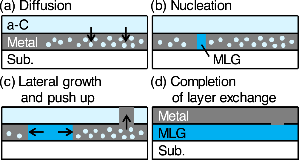
Since the discovery of LE in the Si–Al system more than 20 years ago, the growth mechanism has been well studied both experimentally and theoretically [26–33]. In addition to the Si–Al system, many LE combinations have been reported for semiconductors, such as Si–Ag [34, 35], Si–Au [36, 37], Si–Zn [38], Ge–Al [39, 40], Ge–Ag [41], Ge–Au [42, 43], Ge–Zn [44], and Ge–Sb [45]. These metals are also useful for the LE of amorphous SiGe alloys [46–51]. The LE mechanism is considered to be common for all materials, and carbon is no exception. The LE process is illustrated in figure 1. First, a metal layer and an amorphous carbon (a-C) layer are sequentially prepared on an arbitrary substrate (figure 1(a)). During annealing, carbon atoms diffuse from the amorphous layer into the metal layer, mainly through the metal grain boundaries (figure 1(a)). When the carbon concentration in the metal is supersaturated, MLG nucleates in the metal (figure 1(b)). Later, the carbon atoms dissolved in the metal contact the nuclei, which induces lateral growth (figure 1(c)). The lateral growth stresses the metal and pushes it to the upper layer (figure 1(c)) in a process called the push-up phenomenon. In some studies of the LE in the Si–Al system, in situ microscopic cross-sections and planar images showing push-up phenomena during the LE process were directly observed [29, 52, 53]. Eventually, MLG forms the bottom layer, while the metal forms the upper layer (figure 1(d)). Therefore, MLG is formed during annealing in the LE method, while the starting structure is similar to that in the conventional precipitation during cooling. Thermodynamically, the driving force of the LE process is the difference in the Gibbs free energy between the amorphous and crystalline phases [28, 31]. The metastability and high free energy of the amorphous layer cause supersaturation, which leads to nucleation in the metal layer [29, 32]. Based on the mechanism, there are three conditions for inducing LE during annealing rather than precipitation during cooling. (i) The initial carbon layer should be amorphous or at least poorly crystalline [25, 54], while there are no restrictions on the deposition methods of the carbon layer. (ii) The a-C layer should be thick enough to cause supersaturation of carbon atoms in the metal layer. This means that the film thickness ratio of a-C and metal is important [25]. (iii) The annealing time should be sufficient to induce MLG nucleation in the metal layer, which depends on the annealing temperature. Once the LE is completed, the process does not recur because the MLG formed is completely crystalline. LE occurs even if the order of the layers is inverted [55–57], which enables self-organized formation of the lower electrode [58, 59]. For semiconductors, the inverted-LE has been studied for application in devices with vertical structures such as solar cells [60, 61].

Figure 1. Schematic of the LE process. (a) Diffusion of carbon atoms from the amorphous layer into the metal layer. (b) Nucleation of MLG in metal. (c) Lateral growth of MLG and metal push-up. (d) Completion of LE.
Download figure:
Standard image High-resolution imageAfter LE, the thickness of the MLG formed is almost determined by the initial thickness of the metal layer. Basically, the initial bottom and top layers serve as 'molds' for the eventual top and bottom layers, respectively [62, 63]. We define this phenomenon as LE, which differs from conventional precipitation methods. For the LE of semiconductors, when the amorphous layer is thicker than the metal layer, semiconductor 'islands' form on the bottom-crystalline semiconductor layer, and when the amorphous layer is thinner than the metal layer, the bottom-crystalline semiconductor layer has 'holes', which reduces the coverage of the semiconductor layer on the substrates [64, 65]. Therefore, to obtain uniform MLG, the thicknesses of the a-C and the metal layers should almost be the same. The best way to obtain a high-quality MLG layer with high surface coverage will be to remove the islands in the island-rich samples, which has proven in the LE of semiconductors [66, 67].
2.2. Identification of LE
LE can be identified by examining the cross-sectional structure using focused-ion-beam microscopy, scanning electron microscopy (SEM), and transmission electron microscopy (TEM) with energy dispersive x-ray (EDX) analysis. Raman spectroscopy is also a useful tool for easily identifying LE, especially when the substrate is transparent [22]. Before LE, a-C exists on the front surface and metal on the back surface (figure 2(a)). Therefore, a broad band corresponding to a-C is observed in the Raman spectrum of the front surface, while no peaks are observed in the spectrum of the back surface because of the reflection of the Raman laser by the metal (figure 2(b)). After the LE process, D, G, and G' peaks corresponding to MLG [68] are observed in the Raman spectrum of the back surface, while no peaks are observed in the spectrum of the front surface owing to the metal reflection (figure 2(b)). When the initial a-C layer is thicker than the metal layer, the Raman spectra of the front side of the sample after LE exhibits relatively weak peaks owing to the formation of MLG islands in the upper metal layer [69]. Similar to the LE of semiconductors [67, 70], island MLG has much poorer crystallinity than the bottom MLG layer, which is reflected in the intensity ratio of G to D peaks in the Raman spectra [69]. Depending on the type of metal, LE can be identified by naked eye because the color of the sample surface (and the back surface when the substrate is transparent) changes before and after LE (figure 2(c)) [71, 72]. Metal removal is also useful for identifying LE. When LE is successful, the MLG layer remains on the substrate after the removal of metal by wet etching, which is also visible to the naked eye. More reliably, the remaining layer on the substrate should be evaluated using EDX. The residual metal concentration in the resulting MLG layer is limited by the solid solubility limit of the metal in MLG and is therefore, usually below the detection limit of EDX (∼1%) [22, 71].
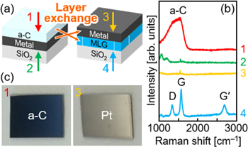
Figure 2. Identification of LE by visual inspection and Raman spectroscopy. (a) Schematic of the samples before and after LE. (b) Raman spectra obtained from the front and back sides of the samples before and after LE using Ni. (c) Photographs of the front surface of the samples before and after LE using Pt. The numbers (1–4) in (b) and (c) correspond to the observation locations in (a). The thicknesses of both the a-C and metal layers are 50 nm. The growth temperature is 800 °C.
Download figure:
Standard image High-resolution image3. Important factors for LE
3.1. Metal species
Most metal-catalyzed graphene syntheses have used transition metals because they are highly reactive owing to their open d-orbitals [73–76]. To date, 15 transition metals (Ni, Co, Fe, Cr, Mn, Ru, Ir, Pt, Ti, Mo, W, Pd, Cu, Ag, and Au) have been examined for LE with carbon [71]. When the stacked structure of a-C/metal/SiO2 substrate, in which the thicknesses of a-C and metal layers are almost the same, is annealed at temperatures up to 1000 °C, the solid-phase reaction that takes place between carbon and metal can be classified into four groups depending on the metal species: (1) LE, (2) carbonization, (3) local MLG formation, and (4) no graphitization (figure 3(a)). The difference in the solid-phase reaction causes large differences in the Raman spectra; a sharp G peak corresponding to highly crystalline MLG appears only in the case of LE (figure 3(b)). Currently, LE for carbon has been confirmed in eight transition metals (Co, Ni, Cr, Mn, Fe, Ru, Ir, and Pt), as summarized in the periodic table in figure 3(c). Generally, early transition metals form more stable carbides [73, 74]; therefore, Ti, Mo, and W form carbides without LE. In contrast, late transition metals tend to form solid carbon solutions. Groups 8−10 have higher carbon solubility than group 11, reflecting the number of electrons in the d orbital [75, 76]. Most of the metals in groups 8−10 induce LE because these metals can dissolve sufficient carbon to cause MLG nucleation in the metal layer. Pd is an exception and cannot induce LE owing to the agglomeration of the Pd layer during annealing. The ease of agglomeration is generally related to the wettability between the metal layer and the substrate. Because Co also easily aggregates, it is difficult to obtain a uniform MLG layer. However, by depositing the Co layer while heating the sample (200 °C) to increase its thermal stability, the LE process is completed before Co is dotted [77]. Changing the substrate material and inserting the underlayer will also be effective in suppressing the aggregation of the metal layer. Therefore, to induce LE of carbon, the metal should (i) have a high solid solubility of carbon, (ii) be stable during annealing, and (iii) not form a carbide. Some metals (Cr, Mn, and Fe) that can form carbides are preceded by LE before carbonization [78]. Considering that only Al, Au, Ag, Zn, and Sb are known to induce LE for Si and Ge, many metals can be used for LE of carbon, despite its short history. This is because carbon is less likely to form compounds than the highly reactive semiconductors.
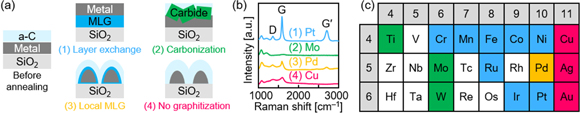
Figure 3. (a) Schematic sample structure, and interactions between metals and a-C classified into four groups. (b) Raman spectra obtained from the back side of the samples after annealing at 1000 °C with various metals (Pt, Mo, Pd, and Cu) representing each group. (c) Elements in the periodic table colored according to the classification in (a). The thicknesses of both the a-C and metal layers are 50 nm.
Download figure:
Standard image High-resolution imageIn the LE of carbon, the metal species also affect the crystallinity of the resulting MLG and the growth temperature, similar to the LE of semiconductors [21, 44]. Annealing at 1000 °C completes the LE of carbon for the above-mentioned eight metals, while the intensity ratio of the G to D peaks in the Raman spectra, which indicates the crystal quality of MLG [79], varies with the metals (figure 4(a)). In addition, the temperature range for LE also depends on the metal species (figure 4(b)). Ni is one of the best metals for low-temperature LE synthesis of MLG. This tendency can be summarized as follows: metals with high carbon solid solubility produce MLG with relatively low crystallinity at low temperatures, whereas metals with low carbon solid solubility produce high-quality MLG at high growth temperatures.

Figure 4. Raman spectroscopy evaluation of the crystal quality of MLG formed by LE using various metals (Cr, Mn, Fe, Co, Ni, Ru, Ir, and Pt). (a) Raman spectra obtained from the back side of the samples annealed at 1000 °C. (b) Growth temperature dependence of the G/D intensity ratio of the samples, derived from the Raman spectra in (a). The higher G/D intensity ratio indicates the higher MLG crystallinity. The thicknesses of both the a-C and metal layers are 50 nm.
Download figure:
Standard image High-resolution imageAs an example, there is a difference in the cross-sectional TEM images of the MLG layers formed by LE with Ni (figures 5(a)–(d)) and Pt (figures 5(e)–(h)). In both cases, MLG is formed on the substrate as a result of LE; however, the shape of the MLG layers is different in the Ni and Pt samples. In the Ni sample, the MLG layer is rippled and contains randomly oriented nanocrystalline carbon in the spaces between the rippled MLG and the Ni layer or substrate (figures 5(a) and (b)) [22]. In contrast, the MLG layer between the Pt layer and the substrate is uniform (figures 5(e) and (f)) [71]. These results account for the difference in crystallinity derived from the Raman spectra (figure 4). The MLG layers are {002} oriented along the film surface for both the Ni and Pt samples (figures 5(c) and (g)). This behavior is consistent with the conventional precipitation methods of MLG: {002} oriented graphene precipitates from metals owing to the minimization of surface or interface free energy [80, 81]. While LE is well known to control the crystal orientation of semiconductor layers even on amorphous substrates [82, 83], the effect is particularly remarkable for MLG, probably because of its large surface energy anisotropy. The selected-area electron diffraction pattern of the Ni sample is arced (figure 5(d)) while that of the Pt sample is spotty (figure 5(h)), reflecting the shape of the MLG layer in each sample. Thus, the type of metal affects the quality of MLG, but the relatively poor crystallinity obtained by Ni-induced LE can be significantly improved by controlling other factors, as described below.

Figure 5. Comparison of the cross-sectional structures of the samples after LE using (a)–(d) Ni at 600 °C and (e)–(h) Pt at 800 °C. (a), (e) Bright-field TEM images. (b), (f) High-resolution lattice images. (c), (g) Dark-field TEM images using the C{002} plane reflection. (d), (h) Selected-area electron diffraction patterns obtained from the regions including the metal and the MLG layers with a selected-area of 200 nm diameter.
Download figure:
Standard image High-resolution image3.2. Annealing conditions
According to the G/D intensity ratio of the Raman spectra (figure 4(b)), the annealing temperature affects the crystallinity of MLG formed by LE. This behavior is well known for any MLG precipitation method [8–10, 13, 19, 25, 81]. For most metals, a higher annealing temperature provides a higher G/D intensity ratio, i.e. higher crystallinity of MLG. This corresponds to the general principle of crystallization: defects in grains decrease as the growth temperature increases, which makes the atoms easier to move. However, this behavior does not apply to some metals, including Ni (figure 4(b)). This is likely because the G/D intensity ratio of the Raman spectra is determined by the balance of intragrain defects and grain boundary defects; lowering the growth temperature increases both the grain size (reducing grain boundaries) of MLG and the intragrain defects. This behavior is well known in solid-phase crystallization, including LE, of semiconductors [21, 84, 85]. In addition, high growth temperatures agglomerate the unstable metal layer, resulting in a rough surface (figure 6) because the metal layer acts as a mold for the MLG (figure 1). Therefore, for some metals, lowering the LE temperature is important for improving the quality of MLG and for a wide range of applications.

Figure 6. Surface morphology of the 50 nm thick MLG layer formed on a SiO2 substrate using Ni-induced LE at growth temperatures of (a) 600 °C, (b) 800 °C, and (c) 1000 °C. The SEM images were recorded after Ni removal.
Download figure:
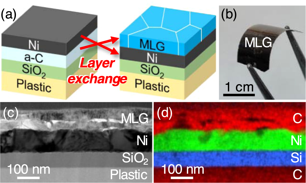
Standard image High-resolution imageThe rate of temperature decrease and the types of inert gases forming the annealing atmosphere are considered as important factors in conventional MLG precipitation methods using solid-phase reaction between carbon and metals [86–88]. The rate of temperature decrease does not affect LE, because the synthesis of MLG is completed during annealing. In addition, the type of inert gas has not been observed to affect the LE synthesis of MLG, similar to the LE of semiconductors. However, atmospheric exposure/non-exposure of the a-C layer has a great influence on the subsequent growth characteristics because the amorphous layer easily absorbs oxygen from the atmosphere. For the Ni-induced LE of carbon, the MLG synthesis temperature is lowered to 350 °C by avoiding air exposure and annealing in a vacuum deposition chamber [89]. The MLG layer formed at 350 °C exhibits higher crystallinity than the MLG layer grown at high temperatures (≥ 600 °C) after air exposure. This growth temperature is lower than the heat resistant temperature of a flexible polyimide substrate, which opens up the possibility of flexible device applications. In fact, MLG can be synthesized on a flexible polyimide substrate by coating a SiO2 layer to prevent the contamination of the a-C layer from the plastic, as shown in figures 7(a) and (b) [90]. In this example, LE with an inverted structure was employed to self-organize the electrodes under MLG (figures 7(c) and (d)) for rechargeable battery applications, as described later.

Figure 7. MLG formed on a plastic substrate using Ni-induced inverted-LE at 350 °C. (a) Schematic of the sample structure. (b) Photograph of the resulting sample. Cross-sectional characterization by (c) bright-field TEM imaging and (d) EDX elemental mapping.
Download figure:
Standard image High-resolution image3.3. Interlayer
The addition of an interlayer between the metal layer and the amorphous layer has been actively studied in the LE of semiconductors [91–94]. This interlayer controls the mutual diffusion of the semiconductor and the metal atoms during annealing. LE does not occur when the metal atoms diffuse into the semiconductor layer before the semiconductor atoms diffuse into the metal layer. Employing an appropriate material as an interlayer can solve this problem and induce LE [95]. Even in a system where LE occurs without an interlayer, diffusion control using an interlayer increases the grain size [96, 97] or aligns the crystal orientations [98, 99]. The use of an interlayer has also been reported to increase the grain size of MLG in conventional precipitation methods [100].
In Ni-induced LE of carbon, SiO2 and AlOx were investigated as an interlayer [69]. In particular, an AlOx interlayer was found to significantly improve the grain size of the resulting MLG layer (figures 8(a) and (b)). The G/D intensity ratio in the Raman spectra, corresponding to the crystallinity of MLG, has a peak depending on the interlayer thickness for both SiO2 and AlOx interlayers (figures 8(c) and (d)). According to TEM analyses, a 1 nm thick AlOx interlayer increases the grain size of MLG to a few micrometers, which is one order of magnitude larger than that of the sample without an interlayer. This is because the interlayer delays the diffusion of carbon atoms into the metal and suppresses MLG nucleation, which gives time for lateral growth of MLG and enlarges the grain size of MLG. Therefore, the improvement in the G/D intensity ratio is considered to basically reflect the increase in the grain size of MLG. When the Al2O3 interlayer is prepared by sputtering an Al2O3 target instead of air exposure of an Al membrane, the G/D intensity ratio increases further (figure 9(a)) [101]. Therefore, the material, thickness, and fabrication process of the interlayer affect the LE properties because they change the degree of interdiffusion between carbon and metal. The crystallinity of MLG can be further improved by controlling these parameters.
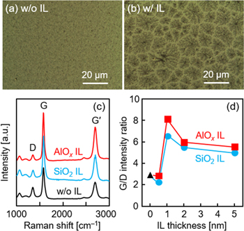
Figure 8. Effects of the interlayer (IL) on the MLG formed by Ni-induced LE at 800 °C. (a), (b) Nomarski optical micrographs for the samples (a) without and (b) with 1 nm thick AlOx IL. (c) Raman spectra obtained from the back side of the samples without and with 1 nm thick AlOx and SiO2 IL. (d) G/D intensity ratio as a function of AlOx and SiO2 IL thickness. The thicknesses of a-C and Ni layers are 75 and 50 nm, respectively.
Download figure:
Standard image High-resolution image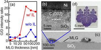
Figure 9. Thickness dependence of the crystal quality of MLG formed by Ni-induced LE at 800 °C. (a) G/D intensity ratio obtained from the Raman spectra of the back side of the samples with and without 2 nm thick Al2O3 interlayer (IL). (b) High-resolution lattice image and (c) bright-field TEM image of the cross-section of 10 nm thick MLG sample before Ni removal. (d) Photograph of the 5 nm thick MLG sample without IL after Ni removal.
Download figure:
Standard image High-resolution image3.4. Thickness
The film thickness of MLG after LE corresponds to the initial film thickness of the metal layer which works as a mold [69]. Therefore, the MLG thickness can be controlled over a wide range by modulating the thickness of the metal layer; this is an advantage over conventional precipitation methods. In fact, Ni-induced LE can be used to synthesize MLG with film thicknesses ranging from 5 to 200 nm [101], which are not the limits of thin and thick layers, respectively.
According to the G/D intensity ratio in the Raman spectra, the crystal quality of MLG is relatively low for MLG thicknesses ≤20 nm and considerably improves at thicknesses ≥50 nm, especially when a diffusion-controlling Al2O3 interlayer is introduced between the a-C and Ni layers (figure 9(a)). It is important to note that the Al2O3 interlayer here is directly deposited using an Al2O3 sputtering target, which provides a higher G/D intensity ratio in the Raman spectra compared to the AlOx interlayer formed by atmospheric exposure (figure 8). The maximum G/D intensity ratio reaches 20, which is higher than that of most MLG layers synthesized on insulators using metal-induced solid-phase crystallization techniques [102–104]. Although the crystal quality of the thin MLG layer is low, it can be formed uniformly on the substrate (figures 9(b) and (c)). The Ni particles on the MLG (figure 9(c)) are attributed to the agglomeration of a thin Ni layer during annealing, which accumulated on the MLG layer after LE. After removing the Ni layer, the thin MLG layer exhibits a high light transmittance (figure 9(d)), which is important for application as transparent conductive films. According to our experiments, it is possible to synthesize MLG with film thickness >500 nm using Ni-induced LE; however, in principle, there is an upper limit to the film thickness that can be obtained by LE. For example, when the Al thickness exceeds 1500 nm in the Si–Al system, the upper Si layer is crystallized before the Si atoms reach the substrate through the Al layer, which inhibits the complete LE [105]. The parameters for realizing thick films using LE are not yet known even in the case of semiconductors; however, the key is to accelerate the diffusion of carbon into the metal. The need for thick MLG layers in various devices will instigate further research in this area.
3.5. Multilayer
LE does not occur when the film thickness of the metal or a-C is smaller than a few nanometers. According to the study on LE of semiconductors [106], this is attributed to the difficulty in nucleation of MLG in the metal layer. Therefore, multilayer structures containing thin a-C or metals can induce LE, resulting in the formation of a uniform MLG layer molded on the initial thick Ni layer (figures 10(a) and (b)). This phenomenon was originally discovered in the LE of semiconductors [107–109] and has also been demonstrated for Ni-induced LE of carbon [110, 111].
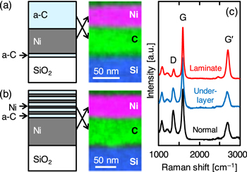
Figure 10. Ni-induced LE of carbon in multilayer structures. Schematics before LE and cross-sectional EDX mappings after LE of the samples with (a) 1 nm thick a-C underlayer and (b) 15 laminated layers of 4 nm thick a-C and 0.5 nm thick Ni. (c) Raman spectra obtained from the back side of the samples with a normal structure, underlayer, and laminated structure after LE at 600 °C.
Download figure:
Standard image High-resolution imageInserting a 1 nm thick a-C underlayer between Ni and the substrate promotes the supersaturation of carbon atoms in Ni and then accelerates the nucleation (figure 10(a)) [110]. This not only lowers the LE temperature, but also enhances the crystal quality of MLG (figure 10(c)). The thickness of the a-C underlayer is important: LE will occur at both the top and bottom sides if the a-C layer is too thick (>5 nm). The a-C/Ni laminated structure also results in uniform MLG as long as the laminated Ni layer is sufficiently thin (figure 10(b)) [111]. The crystal quality of MLG improves dramatically as the number of a-C/Ni multilayers increases: 15 laminated layers of 4 nm thick a-C and 0.5 nm thick Ni result in high G/D intensity ratio in the Raman spectra (figure 10(c)). Thus, the multilayer structure improves the crystal quality of MLG and thereby, its electrical conductivity. This phenomenon is explained by the fact that the interface is the diffusion site of carbon atoms; it promotes the lateral diffusion of carbon atoms and increases the grain size of the MLG [109].
The factors introduced above have already been demonstrated to be effective in the LE of carbon. According to studies on the LE of semiconductors, there are many other parameters that affect the LE of carbon. For example, the underlayer material generally affects LE [112–115]. The qualities of the initial carbon and metal layers are also important factors. Because the carbon atoms diffuse mainly through metal grain boundaries, a metal layer with smaller grains will induce a faster rate (lower growth temperature) of LE [116–118]. Introducing defects [119] or impurities [120, 121] into the a-C layer will also make the carbon bonds in a-C easier to break and promote diffusion of carbon atoms into metals.
4. Device applications
4.1. Electrodes
MLG is a promising material for various applications, including electrodes and heat spreaders, owing to its high electrical and thermal conductivities [122, 123]. Transparent electrodes are the most actively studied application for thin MLG [124–126], while thick MLG is suitable for wiring in integrated circuits because its current-carrying capacity exceeds that of Cu [127–129]. Applications to flexible devices are particularly attractive because MLG is soft and bendable [130, 131]. The ability of LE to synthesize uniform MLG on arbitrary substrates at low temperatures is an excellent feature that helps to incorporate MLG on plastics and in existing devices without damaging them.
Because LE can form MLG uniformly on an insulator, its electrical characteristics can be evaluated easily using Hall effect measurements with the Van der Pauw method [101]. The lower growth temperature tends to provide a higher electrical conductivity (figure 11(a)), which is in contrast to that of most MLG formed by cooling precipitation methods [132–134]. There are two reasons for this: in solid-phase crystallization of amorphous layers, including LE [21, 85], a lower growth temperature provides (i) more uniform crystalline layers (figure 6) and (ii) larger grain size owing to the lower nucleation frequency. This results in lower grain boundary scattering of carriers. It is important to note that, LE is not completed at low temperatures (≤400 °C) unless vacuum annealing avoids air exposure, as mentioned before (figure 7). Both avoidance of air exposure and formation of a-C underlayer appear to be effective in improving the electrical conductivity of MLG (figure 11(a)) as well as lowering the growth temperature [89].
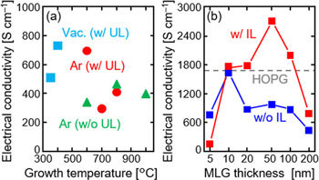
Figure 11. Electrical conductivity of MLG formed on a SiO2 substrate using Ni-induced LE. (a) Growth temperature dependence of the 50 nm thick MLG samples with and without an a-C underlayer (UL); the samples were annealed in an Ar ambient in a tube furnace or vacuum chamber without air exposure. (b) MLG thickness dependence of the samples with and without a 2 nm thick Al2O3 interlayer (IL); the samples were annealed at 800 °C in an Ar ambient. The data for HOPG are shown as dotted lines in (b).
Download figure:
Standard image High-resolution imageThe electrical conductivity of MLG formed by LE also depends on the thickness of MLG (figure 11(b)), which may reflect the balance between contamination from the substrate in the case of thin-film and grain size reduction in the case of thick film [105, 106]. The introduction of the Al2O3 interlayer strongly improves the electrical conductivity owing to grain size enlargement [69, 101]. These behaviors are consistent with the crystal quality of MLG estimated from the G/D intensity ratio in the Raman spectra. The t = 50 nm sample with the interlayer exhibits the highest electrical conductivity of 2700 S cm−1 and showed the highest quality among the LE samples according to the Raman study (figure 4(b)). The electrical conductivity exceeds that of highly oriented pyrolytic graphite (HOPG) with a low mosaic degree of 0.4°, synthesized at 3000 °C or higher. The carrier mobility of MLG reached 550 cm2 V−1 s−1, which is higher than that of most MLG layers formed on insulators, but lower than that of HOPG (960 cm2 V−1 s−1) [101]. The high electrical conductivity of MLG reflects its high carrier density (1019–1020 cm−3); however, it does not imply that the MLG has higher crystallinity than HOPG. Although the origin of the high carrier density in MLG is still unclear, defects and residual Ni in MLG or surface doping by HNO3 solution during Ni removal are possible reasons [135, 136]. The electrical conductivity can be further improved by combining the interlayer and multilayer structures, which will pave the way for application of MLG in electrodes.
4.2. Battery anodes
Graphite has been used as an anode in conventional Li-ion batteries (LIBs) with liquid electrolytes and also shows good anode performance for solid electrolytes [137]. Therefore, an all-solid-state battery using a graphite thin-film, which is a laminated structure of graphene, as the anode increases the feasibility of flexible rechargeable batteries. Although graphene has a high specific surface area and a corresponding high specific capacity [138, 139], MLG with sufficient thickness is desirable for actual anode applications, from the perspective of capacity per area. Because LE enables the synthesis of MLG films much thicker than those obtained from conventional precipitation methods, applications to thin-film rechargeable battery anodes are highly expected [78, 90].
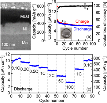
To focus on the evaluation of LIB anode characteristics, MLG needs to be synthesized on a metal substrate. Ni-induced LE at 350 °C with an inverted structure allows formation of MLG on a Mo foil without alloying (figure 12(a)). This structure, with Ni as the lower electrode, is also useful when constructing a thin-film rechargeable battery on an insulating substrate such as plastic. When the sample is packaged in a coin-type cell with a Li foil, an electrolyte, and a separator, the MLG exhibits charge/discharge operation (figure 12(b)). After 50 cycles, the discharge capacity and the Coulombic efficiency reach 6.2 μAh cm−2 and 99%, respectively, and remain stable. Such stable operation is an excellent feature of carbon-based anodes, while there are various candidates for anode materials in all-solid-state batteries. The rate performance shows that the capacity is over 400 mAh g−1 at a current rate of 0.1–2 C (figure 12(c)), which is higher than the theoretical capacity of graphite (372 mAh g−1). This behavior is attributed to the capacitive contribution and reduced diffusion distance of Li ions in local short-range ordered structures [140–142]. Moreover, the capacity retention of the sample is excellent; the capacity assessed during the second 0.1 C measurement almost recovered to that assessed during the first. Although the areal capacity is still small owing to the thin (100 nm) layer of MLG, it can be improved by increasing the MLG thickness. The synthesis temperature (350 °C) for MLG is low enough for the use of plastic substrates, enabling the development of flexible rechargeable batteries.
Figure 12. Anode characteristics of the 100 nm thick MLG formed on a Mo foil using Ni-induced inverted-LE at 350 °C. (a) Cross-sectional SEM image. (b) Cycle dependence of the charge/discharge capacities and Coulombic efficiency at a current rate of 1 C. The inset shows the photograph of the sample packaged in a coin-type cell. (c) Current rate testing at current densities ranging from 0.1 to 10 C; the test was conducted every 10 cycles.
Download figure:
Standard image High-resolution image
5. Summary
We reviewed the latest research on LE of carbon. The mechanism of LE is quite different from that of conventional MLG precipitation methods using metal cooling; the supersaturation of carbon atoms in the metal induces MLG synthesis during heating. The metal species, annealing conditions, interlayer, thickness, and multilayers have been considered as important factors that affect LE, which were summarized in table 1. By controlling these parameters, it is possible to considerably improve the crystallinity, lower the synthesis temperature, and control the film thickness over a wide range. Based on these features, applications to electrodes, including wirings and transparent conductive films, and rechargeable battery anodes were discussed. Applications to flexible devices are highly expected because LE can be used to synthesize high-quality MLG on plastic substrates.
Table 1. Summary of the LE conditions and the resulting MLG properties. Metal is the metal used for LE. t is the thickness of the MLG layer. IL is the interlayer material inserted at the carbon/metal or metal/substrate interface. T is the annealing temperature for LE. IG/ID is the intensity ratio of G to D peaks in the Raman spectra. σ is the electrical conductivity. Remark shows the other parameters discussed in the reference.
| Reference | Metal | t (nm) | IL | T (°C) | IG/ID | σ (S cm−1) | Remark |
|---|---|---|---|---|---|---|---|
| [22] | Ni | 50 | None | 600–1000 | 2.3–2.8 | 330–470 | |
| [69] | Ni | 50 | AlOx , SiO2 | 800 | 2.2–8.1 | 1290 | |
| [71] | 8 types | 50 | None | 600–1000 | 1.3–8.5 | — | |
| [77] | Co | 50 | None | 800 | 1.6–1.9 | — | |
| [78] | Fe | 50 | None | 600–1000 | 2.3–6.2 | — | Anode operation |
| [89] | Ni | 50 | None | 350–800 | 2.6–4.0 | 300–740 | Annealing condition |
| [90] | Ni | 100 | a-C | 350 | 3.8–4.4 | — | Anode operation |
| [101] | Ni | 5–200 | Al2O3, None | 800 | 0.9–21.3 | 160–2700 | |
| [110] | Ni | 50 | a-C | 400–800 | 1.7–4.0 | — | |
| [111] | Ni | 60 | None | 600–800 | 2.4–7.6 | 330–1430 | Multilayer |
6. Future perspective
LE has a history of more than 20 years, but its application to carbon is still in its infancy. Considering that even non-transition metals can induce the LE of semiconductors [21], there are probably many other metals that can induce LE in carbon. There are also many factors that have been verified for the LE of semiconductors but have not been tested for carbon, such as the effects of the quality of the initial carbon and metal layers. Considering that LE is capable of high-concentration doping of semiconductor layers [143–145], the electrical conductivity can be further improved by doping MLG with appropriate elements [146, 147]. It is also interesting to apply the knowledge obtained from analysis of MLG precipitation methods to LE. The critical thickness ratio of a-C and metal that induces LE rather than precipitation during cooling should be clarified. In addition, there is little knowledge about the synthesis of thick MLG films, which are suitable for applications in battery anodes and heat spreaders. The deterioration of crystallinity and electrical conductivity in thin (<10 nm) MLG formed by LE remains a problem to be solved. In addition to those introduced in this article, MLG formed by LE has various potential applications, such as surface emitting lasers [148], sensors [149, 150], passivation layers [151], or supercapacitors [152–154]. Therefore, the LE of carbon still has significant development prospects, both academically and application-wise.
Acknowledgments
The authors acknowledge Professor T Suemasu, University of Tsukuba; Professor N Fukata, NIMS; and Dr N Yoshizawa and Dr Y Kado, AIST for their useful discussions and experimental support. Special thanks are given to the present and past students of University of Tsukuba for their great contributions to the understanding and engineering of LE technology. This work was financially supported by JSPS KAKENHI (Nos. 18K18844 and 18J20904), ATI Research Grants (RG2906), and JST PRESTO (No. JPMJPR17R7).
Data availability statement
The data that support the findings of this study are available upon reasonable request from the authors.