

Abstract
Traditional optical switches relying on the weak, volatile thermo-optic or electro-optic effects of Si or SiN waveguides show a high consumption and large footprint. In this paper, we reported an electric-driven phase change optical switch consisting of a Si waveguide, Ge2Sb2Te5 (GST) thin film and graphene heater suitable for large-scale integration and high-speed switching. The reversible transition between the amorphous and crystalline states was achieved by applying two different voltage pulses of 1.4 V (SET) and 4 V (RESET). The optical performance of the proposed switch showed a high extinction ration of 44–46 dB in a wide spectral range (1525–1575 nm), an effective index variation of Δneff = 0.49 and a mode loss variation of Δα = 15 dB μm−1 at the wavelength of 1550 nm. In thermal simulations, thanks to the ultra-high thermal conductivity of graphene, the proposed switch showed that the consumption for the SET process was only 3.528 pJ with a 1.4 V pulse of 5 ns, while a 4 V pulse of 1.5 ns was needed for RESET process with a consumption of 1.05 nJ. Our work is helpful to analyze the thermal-conduction phase transition process of on-chip phase change optical switches, and the design of the low-energy-consumption switch is conducive to the integrated application of photonic chips.
Export citation and abstract BibTeX RIS
1. Introduction
Nowadays, in order to satisfy the development of optical networks, there is an increasing demand for high-performance optical switches. On-chip photonics switches relying on the weak, volatile thermo-optic [1] or electro-optic [2] effects of Si or SiN usually need a constant supply of the electronic drive circuits, which produce a low refractive index tuning, resulting in large footprint and energy consumption [3]. In order to overcome these challenges, it is very desirable to explore other active photonic materials with strong light modulation and 'self-holding' properties. On this condition, we focused on the optical switches consisted of waveguide and phase change materials (PCMs) [4–6].
PCMs has been widely used in many new fields, such as multi-level storage [7, 8], optical modulator [9], color display [10, 11] and neuro-inspired computing [12] based on the excellent optical properties of PCMs. Chalcogenide PCMs, such as GST, have recently attracted much attention due to its special nonvolatile reconfigurability [13]. During the structural phase transition between covalently bonded amorphous and resonant bonded crystalline states, GST exhibit a significant contrast in aspects of resistivity [14] and optical constants (usually Δn > 1) over a wide spectral range in communication band [15, 16]. The generated state can be retained for more than ten years without any external power supply, which therefore becomes an ideal candidate to realize nonvolatile on-chip micro-photonic devices [17]. In recent years, there has been increased in GST for photonic devices, and a lot of interesting works have been done in photonic device for application targeted for optical switches [18–21] and optical filters [22] at communication wavelength.
In general, phase transition of PCMs on chips can be reversibly actuated by ultrashort optical (picosecond or nanosecond) [23–25] or electrical pulses [26, 27]. The reversible phase transition of GST on the top of waveguide can be driven by physical heating [28] free-space optical heating [29] on-chip optical heating [30] or electric threshold [6, 31] heating. Free-space optical switching, where PCMs are heated by focusing laser pulses in the far field, is not suitable for large-scale integration due to the slow speed, diffraction-limited and inaccurate alignment process. On-chip optical switching, driven by the evanescent coupling of the near-field laser pulse between the waveguide and PCMs, can achieve all-optical operations [32]. However, it is a great challenge to realize the phase transition of large-area PCMs in integrated photonic switching networks because of the inhomogeneous phase transition. Recently, the electric-driven optical switch with external electrodes and heat transfer layers [33] has shown promising results in photonics integrated photonics. Different from the laser heating method, phase change optical switch with external electric heaters can be used to locally select and arbitrarily expand the switching area by increasing the size of the heaters.
In this paper, we designed and optimized an electric-driven phase change optical switch, realizing an ultra-small nonvolatile high-speed and low-energy-consumption on-chip phase change optical switch. The COMSOL Multiphysics was used to calculate the electromagnetic field and temperature field characteristics of the switch. By comparing different electrode materials (Au/Cu/Pd) and heat transfer layer materials (ITO/graphene), we conclude that electrode materials have little effect on the temperature response of the switch. In addition, the temperature field distribution and the energy consumption characteristics of the switch with ITO/graphene heaters in the reversible conversion were analyzed. It is worth noting that the switch with graphene heater has a better heating performance than ITO counterparts.
2. Structure design and modeling
As shown in figure 1(a), the proposed switch is composed of a GST-on-silicon hybrid waveguide based on the silicon-on-insulator (SOI) wafer with a 220 nm thick Si (1 0 0) film on the top of the 3 μm thick buried oxide. The GST thin film with a width of 500 nm, a thickness of 30 nm, and a length of 2 μm is placed on a rectangular Si waveguide with the width of 500 nm. To conduct the electrical switching, electrodes with the thickness of 20 nm are distributed on both sides of the switch, one of which is applied with electric pulse, and the other is grounded. In addition, the applied pulses are assumed to have ideal shapes. In this study, the electrode materials as Au, Cu and Pd, and the heat transfer layer materials including ITO and graphene were compared, respectively.
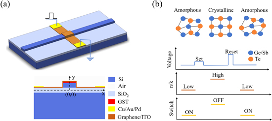
Figure 1. The structure and switching principle of the switch. (a) The 3D structure and the cross-section of the switch. (b) Operation principle of the switch.
Download figure:
Standard image High-resolution imageDifferent from the self-heating method, the electric-driven switch with the heat transfer layer relies on the Joule heat to induce the phase transition of GST. As shown in figure 1(b), for crystallization process, GST was heated above the crystallization threshold temperature (Tg = 433 K) but below melting temperature (Tm = 893 K) [34] by applying a single pulse with low voltage and long pulse width to ensure the complete crystallization of GST, achieving a larger optical constant. For amorphization process, a single pulse with high voltage and short pulse width was applied to electrode in order to heat GST above the melting temperature. And then immediately remove the pulse to achieve quenching effect, making GST return to amorphous state with low optical constant, ensuring the reversible conversion of the switch.
3. Optical performance
3.1. Mode analysis
Based on the frequency domain finite element method (FEM), the optical mode is analyzed by COMSOL Multiphysics (see supporting information). Significant changes in mode profile and effective index ( ) can be observed once GST is switching between amorphous and crystalline phases, showing the remarkable refractive and absorptive modulation effects in the hybrid waveguide. Figures 2(a), (b) show the fundamental quasi-transverse electric (TE) mode of the hybrid waveguide with amorphous GST (a-GST) and crystalline GST (c-GST) at the wavelength of 1550 nm when the thickness of GST is 30 nm. Figure S1 (available online at stacks.iop.org/NANO/32/405201/mmedia) (shown in supporting information) shows the mode profiles of the switch with ITO and graphene heaters. For a-GST, the mode profile is almost bounded in Si waveguide because of the low refractive index. Once the GST is transformed to crystalline phase, as shown in figure 2(b), the mode profile is dramatically moved to the GST film due to the large refractive index, indicating strong evanescent coupling effect, which is consistent with the description of the previous study [35]. Figures 2(c), (d) show the real part of the effective refractive index and mode loss of GST with different thickness and width, respectively. It can be seen that the real part of the effective index and mode loss are positively correlated with the dimensions of GST. The marked dots correspond to the dimensions used in this study (HGST = 30 nm, WGST = 500 nm). Therefore, the difference of the effective refractive index of the fundamental TE mode is 0.49, which is 2.5 times larger than that of the traditional PCM cladding waveguide [36]. The mode losses of the hybrid waveguide with a-GST and c-GST are 0.086 and 14.505 dB μm−1, respectively.

Figure 2. Dependence of optical performance on the dimensions of GST. (a), (b) Normalized electrical field profiled and complex effective index of the fundamental TE mode of the Si-GST hybrid waveguide with a-GST and c-GST. The width and thickness of GST are 500 nm and 30 nm, respectively. (c), (d) Effective index (neff), mode loss (α) and FOM of the Si-GST hybrid waveguide as a function of the thickness and width of GST. The marked points are the parameters used in this study. Here, the width and height of the Si waveguide are fixed to be 500 and 220 nm. Neither the electrodes nor heat transfer layers are involved here.
Download figure:
Standard image High-resolution imageFor nonvolatile phase change optical communication devices, strong light modulation and low insertion loss (IL) are important for the optical performance. Here, we defined an optical figure of merit (FOM), calculated by  ,where
  is the effective refractive index change between the switch with a-GST and c-GST, while
  represents the effective extinction coefficient of the switch with a-GST. The FOM is widely used to characterize the performance of active materials used in switches, and it has been determined to be quantitatively related to IL and switching contrast in all-optical, electro-optical and magneto-optical devices. As FOM does not strongly depend on the dimensions of Si waveguide [37], only the influence of the size of the GST film is discussed here while the width and height of the Si waveguide are fixed to be 500 and 220 nm, respectively. Figures 2(c), (d) show the FOMs variations of the Si-GST hybrid waveguide over the thickness and width of GST. It is evident that the FOM is 202 at the wavelength of 1550 nm when the thickness and width of GST is 30 nm and 500 nm respectively.
3.2. Transmission analysis
Figures 3(a), (b) show the light transmission of the phase change optical switch with a-GST and c-GST, respectively. As for a-GST at the length of 2 μm, the input light propagates through the Si-GST hybrid waveguide with relatively small optical attenuation, leading to 'ON' state (figure 3(a)). With the phase transition to the crystalline state, as shown in figure 3(b), the light propagation is strongly attenuated and almost no optical signal is exported from the output port, forming the 'OFF' state. Both the IL and ER are calculated from the transmission data of the input and output ports, defined as IL = 10 log (Tin/Tout) [38] and ER = ILOFF − ILON, where Tin stands for transmission data of the input port, Tout the transmission data of the output port, ILOFF the IL of the 'OFF' state and ILON the IL of the 'ON' state. In figure 3(c), it can be seen that the loss characteristics of the switch remain stable in a wide spectral range (1525–1575 nm), and the ER is up to 46 dB, indicating a perfect switching contrast. While the IL of the switch with a-GST is about 0.2 dB, meaning an excellent 'ON' performance. Figures S2 and S3 show the IL and ER of the switch with ITO and graphene heaters, respectively.

Figure 3. Transmission characteristics of the phase change optical switch. (a), (b) Light propagations of the switch when GST is in (a) amorphous and (b) crystalline states. (c) The IL and ER of the phase change optical switch as a function of wavelength. Neither the electrodes nor heat transfer layers are involved here.
Download figure:
Standard image High-resolution image4. Thermal performance
In this section, we built up a 2D FEM model to simulate the electrical-driven phase change optical switch with extra heaters based on the COMSOL Multiphysics. The phase transition of GST is induced by Joule heat, for this reason, we use Joule heat module to realize an electro-thermal simulation model, which includes solid heat transfer module and AC/DC module. In this model, electrical simulation predicts the voltage distribution in the device, while thermal simulation is used to obtain the temperature distribution in the device. The heating process based on heat conduction is a non-isothermal process. The simulated material parameters are shown in table 1.
Table 1. Material parameters used in simulations.
| n | k | K (W m−1 K−1) | Cp (J kg−1 K−1) | ρ (kg m−3) | σDC (S m−1) | |
|---|---|---|---|---|---|---|
| Si | 3.48 | 0 | 149 [39] | 720 [39] | 2330 [39] | 100 [39] |
| SiO2 | 1.444 | 0 | 1.38 [39] | 740 [39] | 2200 [39] | 10−14 [39] |
| a-GST | 3.8884 [16] | 0.02469 [16] | 0.27 [40] | 212 [41] | 5900 [42] | — |
| c-GST | 6.6308 [16] | 1.0888 [16] | 0.91 [40] | 212 [41] | 6300 [42] | — |
| ITO | 1.4497 [39] | 0.0923 [39] | 11 [42] | 1290 [42] | 7100 [42] | 2*105 [43] |
| Graphene | 3.2584 [44] | 2.4222 [44] | K(T) [45] | Cp(T) [45] | 2271 [36] | 1000 000 |
n, refractive index. k, extinction coefficient. K, thermal conductivity. Cp, heat capacity at constant pressure. ρ, density. σDC, electrical conductivity. All parameters are for 1550 nm.
In order to explore the influence of heating electrode materials on the temperature field, the transition temperature response curves of ITO (figure 4(a)) and graphene (figure 4(b)) heater with Au, Cu and Pd electrodes materials during crystallization and re-amorphization processes were compared and analyzed. From the temperature curves, it can be seen that the electrode materials have little effect on the temperature change of GST layer. In order to reduce the research cost, Cu electrode was used in the study.

Figure 4. Comparison of the temperature response of the switch with different electrode materials during crystallization and re-amorphization processes. (a) Transient temperature response of the switch with ITO heater. (b) Transient temperature response of the switch with graphene heater. The amplitude and pulse width of the electric pulse are listed in the corresponding figures. Inset: illustration of the applied pulse.
Download figure:
Standard image High-resolution image4.1. Comparison of ITO and graphene heaters
ITO, as an optically transparent material, has higher conductivity and light transmittance, which can be prepared by magnetron sputtering and often used as anti-oxidation layer in optoelectronic integrated devices. As the switch with ITO heater, for SET process, figure 5(a) presents the temperature profile of GST with 20 nm thick ITO heater at the end of a pulse with an amplitude U = 2 V and a pulse width Δt = 40 ns, ensuring that the GST is heated to just above the glass transition temperature (Tg) but below the melting point (Tm), that is the crystallization process of GST. For RESET process, a signal pulse with U = 9 V and Δt = 4 ns was utilized to melt the GST and then rapidly quench, forming the amorphous state with low optical constant. Moreover, figures 5(c), (d) show the transition temperature and the applied pulse as a function of time, which can be seen that the temperature reaches the maximum at the end of the pulse. The energy consumption of the switch was calculated by the formula  where, U, I, t represent the pulse amplitude, the current and the application time of electric pulse respectively. It can be known that in the crystallization process, the required consumption is 0.057 nJ, about 16 times lower than that of the previous study [38], and in the reverse process of transition, the required consumption is 13.13 nJ, which is 1.7 times lower than the previous study.
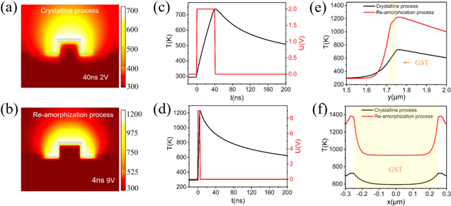
Figure 5. Temperature distribution analysis with ITO heater. (a), (b) Simulated temperature distributions of the switch during crystalline and re-amorphization processes at the end of a pulse, respectively. (c), (d) Pulse application and temperature transition during crystallization process and the re-amorphization process. (e) Temperature profile along the y axis. (f) Temperature profile along the x axis. The yellow-shaded areas in (e), (f) represent the position of the GST film.
Download figure:
Standard image High-resolution imageFigure S4 shows the transient temperature distribution of GST during the SET and RESET processes, respectively. Among them, the vertical lines of different colors show the transient temperature response of GST layers at different time. As a result, the temperature gradient can be represented by the absolute temperature difference (ΔT = Ttop − Tbottom) between the top and bottom GST layer. For SET process, ΔT is about 132 K, while ΔT is about 292 K for RESET process. Figures 5(e), (f) shows the temperature changes along the x and y directions during crystallization and re-amorphization process of the switch, and the yellow-shaded areas represent the position of the GST film. It can be seen that in the x direction, the temperature changes of GST films show a downward-stable-upward trend, and the distribution is symmetrical. This is due to the fact that the left and right sides of GST are close to the heat transfer layer. In addition to the heat transfer from the upper layer, the heat transfer layer on the left and right sides also has an effect on it, resulting in a higher temperature distribution.
Graphene, a single layer of carbon atoms arranged in a honeycomb lattice [45], has many remarkable optoelectronic properties that are highly desirable for photonic applications, such as high intrinsic in-plane thermal conductivity, ultra-low heat capacity, good flexibility and compatibility with the complementary metal oxide semiconductor process [46–48]. Figures 6(a), (b) illustrates the temperature distribution at the falling edge of the electrical pulse of the switch with graphene heater during SET and RESET process. The electrical pulse was set to be 1.4 and 5 ns for crystallization process, while for re-amorphization process, the amplitude was 4.3 V and the pulse width was 700 ps. Figures 6(c), (d) show the temperature change in response to the electrical pulse at the bottom layer of GST. Compared with ITO heater, graphene has excellent heat conduction performance so that amount of heat was transferred from graphene to the GST film in a short time, just requiring a low pulse amplitude or narrow pulse width [45]. Through calculation with  the consumption of SET process is 3.528 pJ, which is 16 time lower than ITO heater above. While the consumption of RESET process is 0.525 nJ, 25 times lower than ITO heater. Figure S5 shows the transition temperature of GST, it can be seen that ΔT of GST layer is small and the overall temperature of the switch tends to be stable rapidly in the cooling process. However, ΔT is lager in the heating process, this is due to the applied time of electric pulse is too short. Figures 6(e), (f) show the temperature curves as a function of different positions of GST. From the red curve in figure 6(f), only the edge of GST layer has reached the melting temperature (Tm). Indeed, a 4 V voltage pulse of 1.5 ns was applied to the switch (figure S6), the temperature of GST was heated above 900 K, and the consumption was calculated as 1.05 nJ. It can be seen the proposed phase change optical switch with graphene heater shows excellent heating performance.

Figure 6. Temperature distribution analysis with graphene heater. (a), (b) Simulated temperature distributions of the switch during crystalline and re-amorphization processes at the end of a pulse, respectively. (c), (d) Pulse application and transition temperature during crystallization process and the re-amorphization process. (e) Temperature profile along the y axis. (f) Temperature profile along the x axis. The yellow-shaded areas in (e), (f) represent the position of the GST film.
Download figure:
Standard image High-resolution image4.2. Transient response analysis
Based on the analyses in section 4.1, we chose graphene heater for subsequent transition response analysis. It is known that the switching speed of the phase change is limited by the pulse width (Δt) and the dead time (τ, 1/e cooling time) because of the thermal relaxation. As the SET process usually requires a much longer pulse which finally determining the transition speed of the switch, we mainly discuss the pulse width and the dead time during the crystalline process. Figures 7(a)–(e) illustrate the normalized transition temperature response with different thicknesses of GST for the amplitude of the pulse is 1 V. It can be seen that the transient response has a high cooling rate for shorter pulse width, which can be understood that for longer pulse width, more energy will be lost to the waveguide and substrate due to thermal diffusion. In addition, the dead time increases with the increase of pulse width, which means that the SET time increases with the increase of pulse width. Figure 7(f) shows the dead time curve as a function of pulse width with a 30 nm thick GST, in this case, the dead time is proportional to the pulse width.

Figure 7. GST thickness-dependent transient response and speed analysis. (a)–(e) Normalized temperature response at the bottom of GST layer for different thickness (10–50 nm) with different electrical pulse width. The amplitude of the pulse was set as 1 V. The dotted line indicates the 1/e position of the maximum temperature. (f) The curve of dead time (τ) corresponding to the pulse width when GST is 30 nm. Inset: illustration of the pulse width (Δt) and dead time (τ).
Download figure:
Standard image High-resolution imageAs presented in figure 8(a), it shows the normalized transient temperature response curve when the electric pulse amplitude is 1 V and the pulse width is 5 ns. Under the same pulse parameters, the temperature response curves of GST with different thicknesses are almost coincident. In addition, as shown in figure 8(b), under the same electric pulse parameters, the dead time curve of GST with different thicknesses is approximately a smooth straight line, which indicates that the dead time is not affected by GST thickness under the same electric pulse parameters. Also, the switch time (Δt + τ) is increasing with the increase of the pulse width, which is consistent with the conclusion in figure 7.
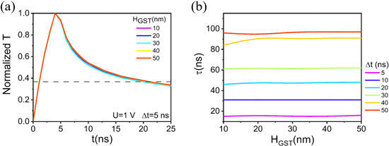
Figure 8. GST thickness-dependent transient response and speed analysis. (a) The normalized transition temperature distribution with different thickness of GST. The parameters of applied electrical pulse are U = 1 V, Δt = 5 ns. (b) The dead time corresponding to different GST thickness under different pulse width.
Download figure:
Standard image High-resolution imageFigure 9(a) presents the amplitude-dependent transient temperature response of the phase change optical switch with a pulse width of 5 ns. It can be comprehended that when the pulse amplitude is 0.6 V, the temperature does not reach the GST crystallization threshold (Tg). However, when the pulse amplitude is 0.8–1.4 V, the temperature is reached crystallization threshold but below the melting temperature (Tm). Figure 9(b) shows the minimum pulse width required for complete crystallization of GST. It can be seen that the minimum pulse width required for complete crystallization decreases rapidly with the increase of pulse amplitude during crystallization process. Considering figures 8(b) and 9(b), the maximum pulse amplitude of 1.4 V should be used during the SET process, while the corresponding pulse width is 5 ns and the dead time is 16 ns.

Figure 9. Amplitude-dependent transient response and speed analysis. (a) The temperature response of GST bottom layer with different pulse amplitudes. Illustration: normalized temperature response corresponding to different pulse amplitude. The dotted line indicates the 1/e position of the maximum temperature. The pulse width is set as 5 ns. (b) The minimum pulse width required for complete crystallization of GST under different pulse amplitudes.
Download figure:
Standard image High-resolution image
4.3. Discussion
The fabrication of the device reported in this paper was based on the methods described in [31, 39] with a little modification. The manufacturing process is combined with a COMS process, fabricated in a SOI wafer. The Si waveguide was patterned by the electron-beam lithography (EBL) and then etched by the reactive ion etching process. The second EBL process was used to form the sputtering window and the GST films were then deposited on it by a magnetron sputtering process followed by lift-off. The electrodes were also patterned by the EBL process and formed by the electron-beam evaporation. The fabrication of the graphene heater was followed by the method described by Ono et al [33].
For the past few years, numerous studies reported the electric-driven phase change optical switch related to the use of ITO or graphene for heating the GST layer [38, 39]. In order to summarize the performance of the proposed switch, the parameter comparison between the switches is further carried out and the results are shown in table 2. By showing the comparative analysis, the switch proposed here showed a better performance in terms of transition speed and energy consumption, which lays a foundation for the low-energy-consumption photonic devices.
Table 2. A comparison of different electrical heaters used for phase change of GST.
| SET process | RESET process | ||||
|---|---|---|---|---|---|
| Device | Heaters | Speed | Energy consumption | Speed | Energy consumption |
| 1 × 1 a | ITO | 40 ns | 0.057 nJ | 4 ns | 13.13 nJ |
| 1 × 1 a | graphene | 5 ns | 3.528 pJ | 1.5 ns | 1.05 nJ |
| 1 × 1 [38] | ITO | 100 ns | 0.9 nJ | 10 ns | 22.8 nJ |
| 1 × 2 [38] | ITO | 100 ns | 5.77 nJ | 10 ns | 38.9 nJ |
| 1 × 1 [31] | PIN diode | 50 μs | 650 nJ | 100 ns | 11 nJ |
| 1 × 2 [18] | ITO | 100 ns | 0.181 nJ | 10 ns | 0.1063 nJ |
| 1 × 1 [39] | ITO | 100 ns | — | 20 ns | — |
5. Conclusion
In summary, we designed an electrical-driven phase change optical switch consisting of a Si waveguide and GST film with ITO or graphene heaters. The switch showed an excellent performance of nonvolatile, high extinction ratio, low-energy-consumption and high-speed. The effective index and mode loss variations as high as Δneff = 0.49 and Δα = 15 dB μm−1 were obtained during the phase transition. Benefiting from the large optical constant contrast of GST, an extinction ratio up to 44–46 dB in a wide spectral range (1525–1575 nm) was achieved. Reversible switching was executed by electrical actuation through ITO or graphene heaters. Compared with ITO and graphene heaters, the switch with graphene had a better heating performance for the SET process with a consumption of 3.528 pJ (16 time lower than ITO heater), induced by a pulse with U = 1.4 V and Δt = 5 ns. While in the case of the RESET process, a 4 V voltage pulse of 1.5 ns was used to heat the GST temperature above the Tm with the consumption of 1.05 nJ, 25 times lower than the ITO heater. To further optimize the optical performance and reduce the IL of the switch, new PCMs with lower extinction coefficient should be used. The electrically driven low-energy-consumption optical switch lays a foundation for realizing integrated network interconnection in the future.
Acknowledgments
This work is supported by the Beijing Natural Science Foundation-Municipal Education Committee Joint Funding Project (Project No. KZ201910005004).
Data availability statement
All data that support the findings of this study are included within the article (and any supplementary files).
Disclosures
The authors declare no conflicts of interest.