

Abstract
High energy and high flux protons are used in proton therapy and the impact of proton radiation is a major reliability concern for electronics and solar cells in low earth orbit as well as in the trapped belts. Carbon nanotubes (CNTs), due to their unique characteristics, have been considered for the construction of proton and other radiation sensors. Here, a single wall CNT based proton sensor was fabricated on FR4 substrate and its response to 150 MeV proton irradiation was studied. The change in the resistance of the nanotubes upon irradiation is exploited as the sensing mechanism and the sensor shows good sensitivity to proton radiation. Proton radiation induces dissociation of ambient oxygen, followed by the adsorption of oxygen species on the nanotube surface, which influences its electrical characteristics. Since the nanotube film is thin and the 150 MeV protons are expected to penetrate into and interact with the substrate, control experiments were conducted to study the impact on FR4 substrate without the nanotubes. The dielectric loss tangent or dissipation factor of FR4 increases after irradiation due to an increase in the cross-linking of the resin arising from the degradation of the polymer network.
Export citation and abstract BibTeX RIS
1. Introduction
Radiation detection using nanomaterials has received attention for developing compact, radiation-resistant detectors with high efficiency, which find applications in particle therapy, reliability of electronics in space, defense and nuclear systems, reliability of solar panels, high energy particle physics and others. Common solid-state radiation detectors operate based on charge collection principle using thick high purity semiconductor crystals. The latter are expensive and the crystal inevitably suffers from displacement damage over time. Nanomaterials in detectors are only a few nm in thickness and offer a low volume but large surface area and thus, rely on mechanisms other than volume-based charge collection such as depolymerization [1], change in dielectric constant [2] and alteration of the surrounding gas ambient [3] upon irradiation. Proton therapy is commonly used now in cancer treatment and employs 50 to few hundred MeV proton beams [4, 5], and monitoring the dose in particle therapy is important for proper treatment. The impact of ionizing radiation on space electronics, satellites and solar cells has long been a concern, and protons are a major constituent in galactic cosmic rays, trapped particles in the van Allen belts and solar particle events [6–10]. A variety of radiation detectors have been introduced over the years [4, 5, 11, 12], which can be mainly categorized into active and passive devices. Active radiation detectors provide real time results whereas the passive detectors must be processed and analyzed later to obtain the results, but they are easy to handle, cheaper and lighter. However, passive devices may not be appropriate for space missions since post analysis in a remote location may be difficult. Active devices are also desirable for proton therapy to provide real time dose assessment. Active devices are extensively used with continued demand for new detectors and sensing approaches, and nanomaterials offer promise in construction of compact and sensitive radiation detectors. For example, during the planning stage of proton therapy treatment, proton computed tomography is used for recording the trajectory of each incident proton using silicon strip detectors. Our experimental findings here show that CNT based detectors can potentially replace the silicon detectors, but further experiments and field evaluation are needed which is beyond the scope of this work.
Carbon nanotubes (CNTs) have been a prominent contender for high-performance radiation sensors due to their attractive properties such as small size, high mechanical strength, robustness, high electrical and thermal conductivity, and high specific surface area [1, 3, 13–17]. Besides detector development, since CNT properties can be readily modified as desired by exposure to various radiations to tailor them for applications, the interaction between CNTs and various radiations and the resulting structural and electrical changes have been extensively studied, for example, electrons [18], ions [19, 20], alpha particles [21], gamma rays [22] and protons [23–28]. The proton radiation studies examined morphological changes of nanotubes upon irradiation of protons at energy levels of 1–10 MeV [23–27]. Boul et al studied the utility of single walled carbon nanotubes (SWCNTs) and several variations including functionalized nanotubes for radiation sensing by examining their resistance change when exposed to 10–35 MeV protons [28] and shown them to be suitable for sensor construction. All of these studies and impact on transistors [8] confirm SWCNTs to be proton-hardened in terms of serious structural damage or breakdown. Impact of high energy protons on nanotubes has not been studied even though energy levels over 100 MeV are common in proton therapy, space missions and detector development. Thus, exploring the impact of high energy protons on SWCNTs and combining with the proven knowledge on their utility for detector design in the low energy range is of value. Here, we present SWCNT based proton detector development along with the change in the nature of the nanotubes upon irradiation of 150 MeV protons characterized by Raman spectroscopy and electrical measurements. Given the nanoscale thickness of the SWCNT film, the high energy proton beam is expected to penetrate deep into the FR4 substrate and therefore, we also investigate the impact of radiation on the substrate as it is most commonly used in printed circuit boards (PCBs).
2. Experimental work
Figure 1 shows the SWCNT based proton detector fabricated on FR-4 substrate. This substrate is a glass-reinforced epoxy laminate composed of woven fiberglass cloth with an epoxy resin. The FR stands for flame retardant and FR-4 is most commonly used in PCBs. For assessing and probing the sensor, circular two-terminal tin-coated copper electrodes were designed on the FR-4 substrate (figure 1(a)) over which the SWCNT was drop cast as shown in figure 1(b). Two electrodes were formed using conventional PCB process and the SWCNT film was deposited by an ink-based dropcasting method. The FR-4 substrate was chemically and physically stable upon adding the SWCNT solution. To study the radiation response, the SWCNT ink containing more than 80% semiconducting nanotubes with diameter ranging from 1 to 1.3 nm in water (KH Chemicals Co.) was diluted with deionized water to produce a loading of 0.01 wt%. Metallic nanotubes are the only impurity in the ink. Further details of the ink preparation and device fabrication process can be found in [3]. The morphology of the nanotubes has been thoroughly characterized previously by scanning electron microscopy and atomic force microscopy in our UV sensor work [16] and therefore, not been repeated.

Figure 1. Optical microscope image of (a) bare sample (electrodes fabricated on FR-4 substrate) and (b) SWCNT based proton detector.
Download figure:
Standard image High-resolution imageThe experimental setup for irradiating the detector is shown in figure 2. Experiments were performed in the Particle Physics and Beam Delivery Core laboratory at Proton and Radiation Therapy Center of Chang Gung Memorial Hospital, Linkou, Taiwan. The sample was mounted on a X–Y stage inside the radiation room and wired to the readout circuit outside the room via electrical feed-through. The readout circuit was designed using Arduino for in situ measurement of the resistance of the nanotube film. A voltage of 5 V was applied to the nanotube film connected in series with a load resistor. The variable resistance of the nanotube film and the constant resistance of the load resistor form a voltage divider circuit, and thus the developed potential on the nanotube was measured, followed by calculating the resistance by Ohms law (see figure 3 for the equivalent circuit). Three samples were tested as detectors with samples 1 and 2 fabricated on a 3.013 mm diameter electrode and sample 3 on a larger 4.126 mm electrode. Each of these samples was irradiated with a proton beam of 150 MeV energy and flux of 1.18 × 10⁸ p cm−2 s−1. This fluence level is relevant to radiation therapy though it may be little high to study radiation impact on electronics with the total admitted dose here being equivalent to several days to few years of exposure in space. The samples were irradiated three times for duration of 3 min each at an interval of 5 min. The resistance of the detector was sampled every 1 s at room temperature of 23 °C.
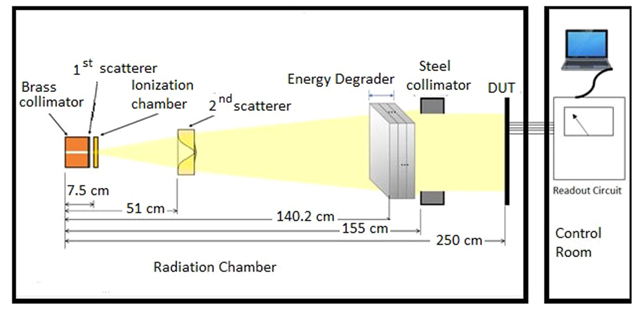
Figure 2. Proton radiation detection experimental setup.
Download figure:
Standard image High-resolution image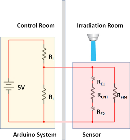
Figure 3. The Arduino system was placed in a control room to avoid the readout circuit experiencing proton irradiation. The supply voltage was 5 V. For load resistor, RL = 1 MΩ was chosen. The input impedance of the Arduino system was approximately RI = 100 MΩ. The total resistance of the sensor consists of two contact resistances (RC1 and RC2) and the CNT film resistance (RCNT). The resistance of the wire and contact electrodes is of the order of μΩ and not exceeding mΩ. The resistance of the FR4 substrate is symbolized by RFR4 and it is an insulator with very high resistance.
Download figure:
Standard image High-resolution imageNanonics Multiview 400 Raman microscope system equipped with a 523 nm laser was used to acquire the Raman spectra of the SWCNTs before and after radiation exposure. Wavenumber calibration was performed using the 520.7 cm−1 line of a silicon wafer and the spectral resolution was ∼1 cm−1. The acquisition time for each spectral region was 1 s with a sub-pixel setting of 3 to enhance band definition by three-fold. The minimum overlap of spectral windows was set to 50, and all spectra was plotted as the average of two accumulations. For the FR4 characterization, the electrical properties were analyzed using Keithley SCS-4200 to examine its permittivity and loss tangent. Fourier transform infrared spectroscopy was also used to examine the change in polymer bonds due to radiation.
3. Results and discussion
Real time resistance measurement was performed to evaluate the performance and durability of the SWCNT based detectors, and also the nanotube characteristics such as defect density and semiconductor-metallic composition were studied before and after proton radiation. The response of the detector is defined as the ratio of change in resistance over the initial resistance of the detector  where R and
  represent the measured resistances after and before radiation, respectively. Figure 4(a) represents the resistance shift as a function of exposure time for the three samples of two different sizes covered with SWCNTs as mentioned before. The detector exhibits a negative resistance shift immediately when proton radiation is turned on and recovers when radiation is turned off. This response here at high energy level, along with similar results in [28] for low energy protons, demonstrates the potential to employ the concept in developing a proton detector for a wide energy range. Figure 4(b) shows the rate of change in percentage change of R (%R) during beam ON for the three samples, and there is a large rate of change in %R during the first cycle with a gradual decrease over the next two cycles, which will be discussed later. There is some sensor-to-sensor variation among the two small electrode samples, and the larger electrode displays larger changes, as expected. Even in identical size small electrodes, the manual dropcasting process results in different amounts of nanotubes and consequently different baseline resistances, leading to unavoidable variations seen in figure 4; these issues will be minimized in automated dropcasting expected to be employed in manufacturing.
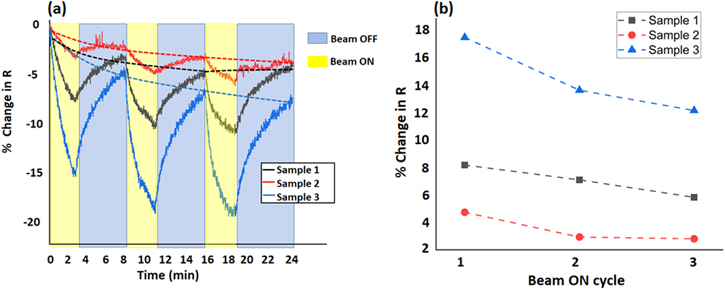
Figure 4. (a) % change in resistance R for the detector samples. The dotted lines show the trend of the decreasing peak resistance of each sample after radiation is turned off; (b) rate of change in % r during beam on. Sample 3 features a 4.126 mm electrode while the other two are on smaller 3.013 mm electrode.
Download figure:
Standard image High-resolution imagePrevious low energy (1–3 MeV) proton studies indicated small changes in morphology of the nanotubes and formation of C–H bonds [23–25]. Raman analysis is a common tool for studying the defects in CNTs and to provide detailed information about chemical structure, phase and polymorphy, crystallinity and molecular interactions. Raman spectra of the SWCNTs are shown in figure 5 for the detector fabricated on the larger electrode (sample 3). The D-peak (1300−1400 cm−1) and G peak (1500−1600 cm−1) in the Raman spectra are of main interest, where D and G represent defect and graphitic regions, respectively. The D-peak intensity indicates the disorder due to the defects induced on sp2 carbon. The ID/IG ratio of the samples obtained after radiation exposure are summarized in table 1 which shows that all the samples are affected by proton irradiation. The increase in the ID/IG ratio could be due to various reasons such as sidewall functionalization of the nanotubes in a chemical environment and defect generation in CNTs due to proton radiation [25, 29, 30].
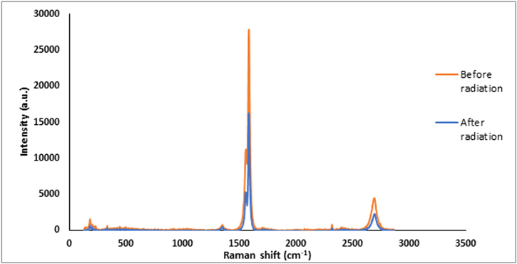
Figure 5. Raman spectra of the SWCNT film before and after proton radiation for sample 3.
Download figure:
Standard image High-resolution imageTable 1.
 ratio before and after 150 MeV proton irradiation.
 (Before) (Before) |
 (After) (After) | %  increase increase | |
|---|---|---|---|
| Sample 1 | 0.02623 | 0.033987 | 29.57204 |
| Sample 2 | 0.020586 | 0.031454 | 52.79183 |
| Sample 3 | 0.019125 | 0.035122 | 83.64006 |
The G peak consists of a main narrow and higher intensity peak denoted by G+, which represents the semiconducting nature of the SWCNTs, and a broad and lower intensity shoulder peak denoted by G− which represents the metallic nature [31]. The samples under investigation are known to possess a mixture of semiconducting (little over 80%) and metallic CNTs (∼20%), hence we have higher G+ peak and lower G− peak as shown in figure 6, which is an expanded view of figure 5 in the wavelength region of 1500–1700 cm−1. Figures 6(b) and (c) shows the left shift of both G peaks, which indicates a change in the composition of SWCNT and the semiconductor to metallic ratio after radiation exposure. Therefore, defect generation and change in the composition of SWCNTs are observed from Raman analysis after proton irradiation.

Figure 6. (a) Raman spectra highlighting the G peak from sample 3 (enlarged view of the data in figure 5) and (b) and (c) show Raman shift for both G peaks representing the shift in composition of the SWCNTs (semiconductor to metallic ratio).
Download figure:
Standard image High-resolution imageIntroduction of defects by radiation impact would be expected to alter the conductivity of the nanotube network with the extent dependent upon radiation energy and fluence and film thickness. The defects on the nanotube surface can serve as sites to assist carrier hopping. These are direct effects of defects on resistance change, which will be shown to be small here. Figure 4 shows a negative resistance shift upon irradiation here. Adsorption of ozone molecules and other oxygen species−generated by radiation impact of the ambient surrounding the nanotubes−on the defect sites of the nanotube surface has been shown to cause a decrease in the resistance when CNT samples were irradiated with high energy gamma radiation [3]. Ozone can also be generated when high energy proton beams strike the oxygen molecules in the ambient [32, 33]. Thus, the ozone-mediated mechanism is thought to be responsible here also for the observed drop in resistance upon proton irradiation as in the case of gamma radiation [3]. As the proton beam is turned off, desorption of these adsorbed species follows, which renders the resistance of the SWCNTs to recover as seen in figure 4. This hypothesis was verified here by conducting control experiments as described next. A set of three samples were fabricated where the SWCNTs were covered with a polydimethyl siloxane (PDMS) film, thus isolating the active sensing region from the ambient air whereas the active region was fully exposed to air in the corresponding naked samples discussed thus far. A liquid based PDMS was coated on the nanotubes followed by thermal curing, and this PDMS acted as passivation for the CNTs, effectively blocking the adsorption of ozone onto the CNTs. Figure 7 shows the schematic illustration of CNT samples with and without PDMS and their resistance change during irradiation. Much lower resistance change was observed for the sample covered with PDMS compared with that for the naked CNT sample. This shows that proton radiation can still pass through the PDMS coating, causing defect formation and changing SWCNT composition as discussed before, but may be at a reduced severity as evidenced by the smaller change in resistance. The overall resistance change is ∼2% instead of 8% for the naked samples, suggesting adsorption of ozone to be the dominant mechanism for the change in resistance of the sensor.

Figure 7. (a) Schematic illustration of the test CNT samples with and without PDMS coating and (b) variation in % resistance change for the samples with and without PDMS coating.
Download figure:
Standard image High-resolution imageThe defects contribute indirectly to the resistance change as they provide preferred sites for adsorption of oxygen-containing groups under the above mechanism. The ozone adsorption is proportional to the defect density, i.e. more defects render more ozone adsorption, resulting in higher resistance change. In other words, one cannot separate the contribution of radiation defects and ozone adsorption to the resistance change. Table 2 shows the change in ID/IG ratio (representing defects) and the change in resistance for all three samples for three cycles. In all cases, the maximum resistance change coincides with the maximum defects. The relationship between ID/IG ratio and % change in resistance for cycle 3 (last column of table 2) is linear given by y = 0.1784x–2.9458 with an R2 of 0.98803, where y is the % resistance change and x is ID/IG ratio. The relations are similarly linear in other cycles too.
Table 2.
 ratio and % change in resistance before and after 150 MeV proton irradiation.
| % change in R | ||||
|---|---|---|---|---|
| % increase in ID/IG after radiation | Cycle 1 | Cycle 2 | Cycle 3 | |
| Sample 1 | 29.57204 | 4.76 | 2.54 | 2.68 |
| Sample 2 | 52.79183 | 8.23 | 7.14 | 5.86 |
| Sample 3 | 83.64006 | 17.61 | 13.73 | 12.24 |
It is important to make sure that any possible Joule heating due to the applied 5 V during the Arduino measurement does not contribute to the observed adsorption/desorption behavior. Picozzi et al studied the adsorption of ozone on CNTs for developing an ozone sensor and discovered that the resistance of CNTs decreases at different ozone concentrations with the recovery dependent on temperature, upon switching off the ozone source [34]. Similar results were reported by Wongwiriyapan et al when SWCNTs were exposed to ozone with the resistance measured at a constant voltage of 200 mV; the resistance recovered to the initial value due to desorption of ozone when the sample was heated and ozone was switched off [35]. CNT based electrothermal heaters have been shown to be capable of generating a heating rate of up to 6.1 °C s−1 at 35 V from the SWCNT film [36]. Based on this data, we expect a temperature rise of about 0.8 °C (∼7 times smaller) since our measurement was conducted at a constant voltage of 5 V. To verify this estimate, we measured the temperature of a SWCNT layer when 5 V supply was supplied to the device under test for 10 min at room temperature (23 °C), and a temperature rise of 0.7 °C was observed as shown in figure 8. This level of self-heating is too small to have any impact on the observed characteristics. Any possible temperature rise due to the incident proton beam is also estimated to be only few degrees, based on previous studies [28] and thus, not expected to have any impact.
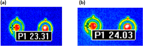
Figure 8. Temperature rise in SWCNT samples (a) before and (b) after 5 V supply is provided to the samples.
Download figure:
Standard image High-resolution imageThe observed behavior of declining rate of change over time in figure 4 is consistent with the proposed ozone-mediated mechanism and is routinely seen in gas sensors. Incomplete recovery to baseline due to slow desorption upon removal of the source is the known reason for this and UV-assisted rapid recovery has been advocated for remediation of this issue in CNT gas sensors. Mild level of heating may be appropriate here, as suggested in previous ozone sensor development [35]. A sensor operating under this mechanism may not work in vacuum environment of space due to the absence of oxygen ambient but the sensor encapsulation in figure 7 may be modified to trap a volume of air which can provide a fixed ambient with air; indeed, this would provide an added advantage of a static background as opposed to a dynamic changing ambient environment seen in the left image of figure 7(a). A single sensor of this type is useful to monitor proton beams in controlled environment such as in proton therapy. Complex space environments with several radiation types would require a sensor array with multiple materials or variations of SWCNTs involving doping, functionalization, metallization and other strategies [28]. This array approach is needed because pristine CNTs respond to many radiations (and also gases) in the form of resistance change; then, selectivity in terms of type and fluence of radiation as well as even simple conversion of the recorded resistance change to radiation units would need a sensor array or radiation nose [2] that can give orthogonal responses with multiple materials, aided by machine learning. Since the sensor in this work is irradiated with only one energy and the results show that it could be employed as a high energy proton sensor, further experiments will be needed to study the response of the sensor at different energies and doses in order to confirm its usage as dosimeter.
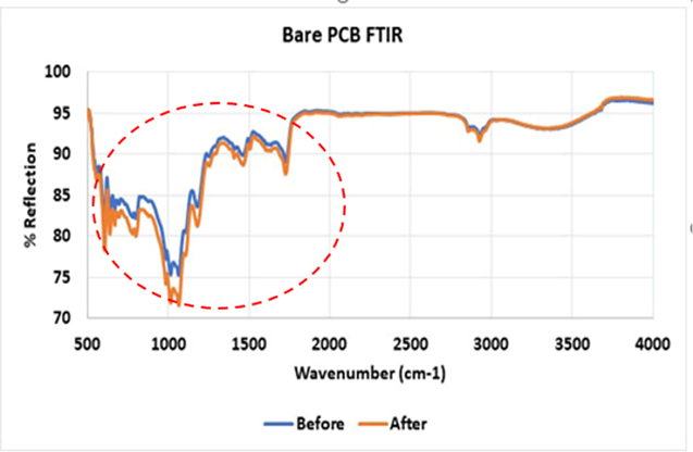
Finally, it is important to examine the impact of radiation on the substrate as well, since the nanotube film is very thin and the proton beam is expected to penetrate deep into the substrate depending on the energy level. SRIM (stopping and range of ions into matter) calculations have shown the projected range for 10–35 MeV protons to be 5 mm deep into the material [7] and this range could be even longer under the present conditions. Thus, the effect of 150 MeV protons on the substrate is also of interest. Though any change in resistance of the FR4, which is an insulator, will not affect the sensor performance according to the equivalent circuit in figure 3, studying the impact is of interest due its wide use in PCBs. Information related to x-ray and neutron radiation effects on the FR-4 substrate is available [37, 38], but not for proton radiation. To study the impact of proton radiation on FR-4 substrate, a sample similar to the sensor shown in figure 1(a) but without the nanotubes was subjected to the same proton beam energy and ON–OFF profile. Measuring the dielectric loss tangent before and after the irradiation provides information about the electrical loss. The loss tangent was measured at room temperature of 24 °C with a DC bias voltage of 1 V and frequency range of 100 kHz to 500 kHz using a Keithley SCS-4200 measurement equipment. The test condition was chosen for the maximum detection sensitivity of the change in the loss tangent. The loss tangent (or dissipation factor) of the FR-4 substrate was found to increase for all samples after irradiation as shown in table 3 with the larger sample showing larger changes. This increase is due to the formation of mobile charge carriers or orientable dipolar molecules that can conduct electric current [39]. These charge carriers or dipole molecules are formed due to the alteration in the structure of the substrate material due to irradiation. To further understand the increase in the loss tangent of PCB, figure 9 shows the FTIR results of the PCB before and after irradiation. No new peak is observed after irradiation indicating the absence of new byproducts following radiation [40]. However, changes in the intensity level in the wavelength range from 600 cm−1 to 2000 cm−1 are evident, indicating that the variation in the FR4 material properties is mainly attributed due to an increase in the cross-linking of the resin system and degradation in the polymer network [41].
Table 3. Loss tangent of the FR4 PCB samples without nanotubes before and after 150 MeV proton irradiation.
| Loss tangent | |||
|---|---|---|---|
| Sample number | Before | After | % change |
| Sample 1 | 0.0211 | 0.0219 | 3.8 |
| Sample 2 | 0.0211 | 0.0214 | 1.4 |
| Sample 3 | 0.022 | 0.0281 | 27.7 |
Figure 9. FR-4 (without nanotubes) FTIR results before and after 150 MeV proton irradiation.
Download figure:
Standard image High-resolution image
4. Conclusion
A SWCNT based proton sensor was fabricated on FR4 substrate and its performance was studied under 150 MeV of proton irradiation by in situ resistance measurement. The results show that SWCNTs are sensitive to high energy proton radiation and can be employed as active material in sensor construction, since they are already known to be useful in the few MeV energy range. The response of the sensor is influenced by the adsorption of ozone molecules and other oxygen species, created by the interaction of protons with the ambient, at the nanotube surface. This ozone-assisted resistance change mechanism was verified by comparing control PDMS-coated SWCNT samples to naked nanotube samples upon proton irradiation. The PDMS-coated samples showed no significant change in resistance, as the coating is not permeable to the ambient and prevents the production and availability of ozone and related species. The FR4 substrate and simple printing process make these sensors inexpensive to produce and thus, could even be considered for disposable applications. Future studies must consider an array of sensors with material variations to distinguish the types and energy/fluence levels of various radiations with the aid of machine learning.
Acknowledgments
Particle Physics and Beam Delivery Core Laboratory of the Institute for Radiological Research, Chang Gung University/Chang Gung Memorial Hospital, Linkou, Taiwan is acknowledged for providing access to conduct the proton irradiation experiments. The work at Ames was supported by the In Space Manufacturing Program of the Space Technology Mission Directorate (STMD) and the Advanced Exploration Systems (AES) Office of the NASA Human Exploration and Operations Mission Directorate (HEOMD).
Data availability statement
All data that support the findings of this study are included within the article (and any supplementary files).