

Abstract
Plasmonic nanostructures are successfully demonstrated in solar cells due to their broad spectra-selective resonance in the range of ultraviolet to near-infrared, and thus light absorption can be mostly improved and power conversion efficiency (PCE) further. Here, we demonstrate plasmonic dye-sensitized solar cells (DSSCs) using collapsible Au nanofingers to build photoanode to enhance light absorption. In this plasmonic DSSCs, by balancing local field enhancement due to gap-plasmon resonance and dye fluorescence quenching, the optimal gap size in collapsed Au/Al2O3/Au nanofingers is designed by twice the Al2O3 thickness and then deposited a TiO2 layer as photoanode. The results show that the PCE of DSSCs is mostly improved as compared to DSSCs with photoanode of Au/Al2O3/TiO2 films, which can be ascribed to the coupled local field enhancement within the sub-nanometer gaps. In addition, fluorescence of dyes on plasmonic nanofingers is nearly 10 times higher than plain Au/Al2O3/TiO2 films, which further proves the dye absorption enhancement. These plasmonic nanofingers enable the precise engineering of gap-plasmon modes and can be scaled up to wafer scale with low cost by the nanoimprint lithography technique, which suggests the feasibility of applying our result in constructing the photoanode for other types of solar cells.
Export citation and abstract BibTeX RIS
1. Introduction
The demands for clean, renewable energy sources have become one of the mostly urgent issues for our society. Utilization of solar energy through photovoltaic technology is a solution. A variety of photovoltaic devices are developed in past years, such as, silicon solar cells, dye-sensitized solar cells (DSSCs), perovskite solar cells etc [1–6]. In order to improve the performance of solar cells, the new techniques which mainly include structural design, new materials, efficiently and highly stable dyes, have been developed to improve the light trapping and power conversion efficiency (PCE) further [7–11]. Among them, plasmonic solar cells are an attractive technology because plasmonic nanostructures at resonant excitations can efficiently trap the incident light within nanoscale space and form an extremely strong local electromagnetic (EM) field near the surface of nanostructures, and thus efficiently enhance the Sunlight absorption [12–14]. DSSCs contains photoanode, counter electrode, electrolyte and dyes in which dye-sensitized photoanode absorbs sunlight to generate electrons. At present, plasmonic nanoparticles are broadly investigated to design photoanode of DSSCs so that the extinction of dye can be mostly increased, leading to a high PCE [15–18]. However, the distribution of metal nanoparticles in TiO2 network is not uniform due to the reproducibility in fabrication over a large area. Therefore a design of ordered plasmonic nanostructure is necessary.
Metallic gap-structures with gap-plasmon resonance can produce an extremely strong EM field within a sub-nanometer gap that is decided by both the classical EM theory and quantum mechanics [19–26]. For example, the aggregates of metal nanoparticles could create nanometer junctions with maximum enhancement of (E/Ein )2 up to 106 fold [27, 28]. However, to achieve the optimized enhancement decided by quantum plasmons, the fabrication of ordered nanostructures with atomic precision of tunable gap is still a challenge. Most conventional methods including electron-beam lithography and physical etching for creating sub-nanometer gap are constrained by the lithography resolution limit [29–35]. Thus, precise tailoring of the gap size at sub-nanometer scale over a large area is critical to form strong and reproducible enhanced EM field. On the other hand, emission quenching of dyes is associated with the direct contact between the dye and the metal, which is decided by the separation distance between the metal and the dye [17, 18]. It has been demonstrated that the optimal separation distance is at sub-5 nm scale [36, 37]. Therefore, the construction of ordered plasmonic nanostructures with high EM field enhancements and the control of dye-metal distance are very important to enhance the efficiency of plasmonic DSSCs. Previously we demonstrated the collapsible nanofingers that show strong EM field enhancement by precisely controlling the gap size at the sub-nanometer scale. This collapsible nanofingers could be fabricated over large area by nanoimprint lithography (NIL), reactive-ion etching (RIE) and atomic-layer deposition (ALD) [24]. The flexible Au nanofinger matrix have a high aspect ratio, and each nanofinger is composed of a polymer nanopillar capped with an Au nanodisk. The subsequent dielectric layer coating on the nanofingers and collapse process can realize the precisely tuning of gap size by twice the thickness of dielectric layer.
In present work, the collapsible nanofingers are studied to design a photoanode in DSSCs, which can precisely control the gap size and the dye-metal distance, achieving high reliability and high throughput at low cost [24, 38–41]. First, a thin conformal Al2O3 layer of 2.5 nm is deposited uniformly by ALD onto flexible Au nanofingers. Through exposing them to ethanol, a 5 nm nanogap is formed under capillary force [24]. Second, the collapsed Au/Al2O3/Au nanofingers are further deposited with a 2 nm TiO2 film as the photoanode. The configuration of plasmonic DSSCs containing both dye and electrodes is shown in figure 1(a), in which the electrolyte is typically I−/I−3. Upon the absorption of sunlight, the dye injects an electron into the TiO2 network. The electron travels through this network until it is collected. The resulting dye radical is reduced to its ground state by a redox process of I−/I3−, as shown in figure 1(b) [17]. In this plasmonic DSSCs, the resulting extremely strong local EM field through collapsed Au/Al2O3/Au nanofingers can improve the absorption of incident sunlight and the extinction of dyes simultaneously, which leads to a high enhancement of PCE. The results show that the PCE is mostly improved as compared to the normal photoanode of Au/Al2O3/TiO2. This new structure with low cost is also applicable to other types of solar cells.

Figure 1. Schematic configuration of Plasmonic DSSCs under illumination of sunlight. (a) DSSCs consist of a photoanode that is fabricated by 2 nm TiO2 film deposited on the collapsed Au/Al2O3/Au nanofingers with 5 nm gap, and a counter electrode with ITO glass. (b) Schematic electrons traveling into the TiO2 photoanode network and a redox process typically by I−/I3− electrolyte.
Download figure:
Standard image High-resolution image2. Experimental sections
2.1. Fabrication of Nanofingers array and DSSCs assembly
The fabrication of high-density arrays of Au nanofingers with flexible polymer support on the glass substrates was referred in our previous report [24, 40]. First, high-density arrays of Au nanofinger with a flexible polymer support on the plain glass were fabricated by our well-developed NIL method. To get the tetramer nanostructures in the subsequent collapse process, the Au films were deposited at a normal incidence to form Au nanodisks and the height of nanofingers were controlled with 300 nm. As compared to dimeric structures, the tetrameric structures can realize the independence of polarization and much more hotspots so that the Sunlight absorption can be efficiently enhanced. Subsequently, an ultrathin 2.5 nm Al2O3 film was deposited on them via ALD (Ultratech Simply ALD). Thirdly, the Au nanofingers were soaked into ethanol and then air-dried at room temperature, which form tetramer nanostructures by a group of four nanofingers through the microcapillary force, and Van der Waals forces kept these tetramer nanofingers from separating once they collapse [24]. Finally, a 2 nm amorphous TiO2 was deposited on the collapsed nanofingers by ALD to form the photoanode. For comparison, we fabricated another photoanode by depositing the Au film, Al2O3 film and TiO2 film on the plain glass with the same parameters.
The DSSCs assembly is shown in the following procedure. Dissolving 5.3 mg of N719 dye in 15 ml ethanol to prepare a 0.3 mM dye solution and then the dye solution was injected into test cubes with equal 5 ml by syringe [42–46]. The conductive wire connected to the feedthrough from the surface of TiO2 film in the photoanode. After immersed into the 0.3 mM N719 dye solution for 10 h for sensitization, the samples were cleaned with ethanol and dried with N2 gas. The counter electrode was the ITO glass substrates with 2 nm Pt layer deposited by ALD which kept the high transparency to incident sunlight. Then dropping the iodide/triiodide (I−/I3−) electrolyte to the photoanode sensitized by N719 dyes, putting counter electrode on the whole assembly and clamping the two parts with two bookends. Finally, the DSSCs was finished as a solar cell under the illumination in sunlight.
2.2. SEM and fluorescence measurements
SEM images were taken by an SEM (Hitachi, S4800) operating at an accelerating voltage of 2 kV and an average working distance of 8.2 mm. Fluorescence spectra of N719 dyes were performed by a Renishaw inVia Raman microscope. The laser excitation wavelength was 514 nm, and a 50X standard objective was used and the spot focus mode was selected. The incident light polarization was along the dimer direction.
2.3. DSSCs solar cell data measurements
The I–V characteristics of the DSSCs were measured under sunlight conditions (AM1.5 G, 100 mW cm−2), with a xenon lamp light source equipped with the Oriel Sol3A Class AAA solar simulator (Newport, USA). During the I–V measurements, we adjusted the active area of DSSCs to 0.25 cm2.
3. Results and discussion
Plasmonic DSSCs based on the collapsed Au nanofingers are mainly described in the experimental sections. In the collapsed Au/Al2O3/Au nanofingers, the gap size is precisely defined by twice the Al2O3 thickness, which is 5 nm. Since the tunneling barrier height is 2.52 eV that is defined by the difference between the Fermi level of Au (5.1 eV) and the electron affinity of Al2O3 layer (2.58 eV), the strongest field enhancement occurs at a 2 nm Al2O3 dielectric gap determined by classical EM theory and quantum mechanics [24]. However, by considering fluorescence quenching, we have demonstrated that 5 nm Al2O3 dielectric gap is the optimal distance [47]. Thus, a 2.5 nm Al2O3 dielectric film is deposited here to realize 5 nm nanogap. It is noted that a 2 nm amorphous TiO2 layer is successfully proved to afford efficient electron transport in DSSCs and thus 2 nm TiO2 layer is selected [17]. Furthermore, since the Al2O3 layer has the lower permittivity than TiO2 film, thicker high permittivity TiO2 film will lead the EM field to be much more confined inside of the dielectric gap, which is not useful to the extinction of dyes. In addition, Al2O3 layer can provide a higher tunneling barrier and a stronger screening for the radiation field than TiO2, which leads to strong fluorescence enhancement for a dye [47, 48]. Therefore, we combine a 2.5 nm Al2O3 layer with a 2 nm TiO2 layer to construct the photoanode in which the 2 nm amorphous TiO2 layer only affords efficient electron transport network in DSSCs.
Figure 2(a) shows a scanning electron microscopy (SEM) image of 2.5 nm Al2O3 coated Au nanofingers prior to the collapsing process. The diameter and height of each nanofinger are 70 nm and 300 nm, and the lattice spacing is 130 nm. The lattice spacing and Au cap size can be adjusted by the designed mold with atomic precision, which is fabricated by double interference lithography. Through the collapsing process, the nanofingers with the height of nearly 300 nm tend to form tetramer Au/Al2O3/Au nanostructures. The coverage of Al2O3 film on the Au tip of nanofinger was demonstrated by cross-sectional TEM in our previous result [24]. Based on this tetramer Au/Al2O3/Au nanofingers, a 2 nm TiO2 layer is coated on their surface, as shown in figure 2(b). In addition, some nanofingers at a small area with the defects of remaining a single nanofinger have not collapsed due to the uniformity of RIE etching process, as shown in figure 2(b). However, for such large area, the effect of these defects on the performance of DSSCs are very small. To study the optical properties of collapsed nanofingers, the reflectance spectra are measured, as shown in figure 2(c). The results show that the collapsed Au/Al2O3/Au nanofingers have a resonance band centered at approximately 660 nm, which can be ascribed to the bonding mode of the localized surface plasmon resonance (LSPR) of Au caps coupling each other to form bonding-LSPR [40], as shown by the black line in figure 2(c). After the deposition of TiO2 film, the TiO2–Au/Al2O3/Au nanostructures show a little redshift and is centered approximately at 670 nm, as shown by the red lines in figure 2(c). This little difference in the central wavelength for the coupled bonding-LSPR is ascribed to high index of TiO2 films. The resonance can cover a broadband range from ∼550 to ∼800 nm which is consistent with energy spectra of sunlight. For comparison, the photoanode of Au/Al2O3/TiO2 films on the plain glass has small response to the spectra range for the Sunlight, as shown by the blue line in figure 2(c). Therefore, the plasmonic nanostructure can induce scattering and absorption which can enhance the Sunlight absorption. To quantitatively demonstrate EM field enhancements in collapsed nanofingers, we run simulations for near-filed distribution and localized EM field enhancement using a commercial finite-element method-based software package (COMSOL Multiphysics). The permittivity of Au is interpolated from the experimental data [49], and the refractive index of the polymer support is set as 1.48 [39]. The 660 nm plane waves that is at the resonance condition is polarized parallel to the gap direction, which corresponds to bonging-LSPR [50]. The cross-sectional distribution of coupled EM field for the tetramer Au/Al2O3/Au nanofingers is depicted in figure 2(d). It shows that the strong EM field between the two approaching Au/Al2O3 nanofingers is ascribed to hybridization of the dipole resonances into the bonding-dipole plasmon modes. In this case, the local electric field enhancement ((E/Einc )2), reaches up to ∼104. In addition, at the non-resonance of 540 nm due to the absorption of N719 dye, the local EM field enhancement ((E/Einc )2) at the dielectric area is ∼100-fold due to the coupling of surface charge as shown in figure S2 (supporting information) (available online at stacks.iop.org/NANO/32/355301/mmedia). Therefore, by plasmonic nanofingers, the incident photons efficiency can be improved, and the charge carrier density for the sensitizing dyes can be further boosted. It is noted that in our design, since the tunneling barrier heights for Au/Al2O3 and Au/TiO2 are 2.58 eV and 0.9 eV, respectively, and thus the near-field EM enhancement to dyes emissions process dominates the electrons injection to TiO2 network, and hot electrons injection from Au to TiO2 network is not major contribution [48].
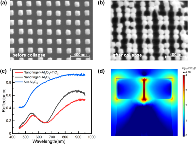
Figure 2. SEM and Optical properties for the photoanode of TiO2–Au/Al2O3/Au nanofingers. (a) SEM image of Au nanofingers matrix. (b) SEM side view image of TiO2–Au/Al2O3/Au nanofingers. (c) Reflectance spectra measurements. Red line presents the TiO2–Au/Al2O3/Au collapsed nanofingers; Black line presents the Au/Al2O3/Au collapsed nanofingers; blue line presents the Au/Al2O3/TiO2 composite films. (d) Cross-sectional distribution of the EM field on the TiO2–Au/Al2O3/Au nanofingers at 660 nm.
Download figure:
Standard image High-resolution imageTo investigate the performance of plasmonic DSSCs, we carried out the measurements. A full list of the solar cells data is shown in table S1 (supporting information). Figure 3(a) shows the picture of assembled DSSCs, in which the red one represents plasmonic DSSCs based on the collapsed Au nanofingers and the blue one is DSSCs based on the photoanode of Au/Al2O3/TiO2 films (noted as normal DSSCs) for comparison. The current of the device can be measured when it is electrical biased and sunlight illuminated [51]. During the current density–voltage (J–V) measurements, the active area of DSSCs is set to 0.25 cm2. The J–V characteristics of DSSCs are measured under sunlight conditions (AM1.5 G, 100 mW cm−2, with a xenon lamp light source). Figure 3(b) shows the J–V curves of DSSCs. To clearly observe, the curve in the green dotted square region in figure 3(b) is zoomed in and shown in figure 3(c). The fluctuation of J–V curve for normal DSSCs may due to the quality of the deposited film. It is clearly seen that the open circuit voltage (Voc ) of plasmonic DSSCs increases from 0.50 to 0.73 V, and the Jsc increases from 0.058 mA cm−2 to 0.136 mA cm−2, as compared to normal DSSCs. Further, for our plasmonic DSSCs, the PCE improves from 0.01% to 0.03% (as shown in table S1), and the maximum power output (Pmax) enhances from 2.7 μw to 6.5 μw as shown in figure 3(d). The enhancements of PCE and the Pmax are consistent with the trend of the Jsc improvement for plasmonic DSSCs. In our design, since TiO2 layer is directly deposited on the collapsed nanofingers, the sensitized surface area is not increased by compared to normal DSSCs and the enhancement of Jsc in plasmonic DSSCs is mainly due to the improvement of sunlight absorption. Therefore, the improvements of the PCE and Pmax are mainly induced by plasmonic nanofingers.

Figure 3. Characterizations of plasmonic DSSCs. (a) Photo of fabricated DSSCs. Red one represents DSSCs based on the collapsed Au nanofingers (defined as plasmonic DSSCs) and the blue one is DSSCs based on the photoanode of Au/Al2O3/TiO2 films(defined as normal DSSCs). (b) Photocurrent density–voltage plot of DSSCs with photoanodes of TiO2–Au/Al2O3/Au nanofingers (red dot line), and Au/Al2O3/TiO2 composite films (blue line). (c) Magnification of Photocurrent density–voltage plot of DSSCs for green rectangular dot line in (b). (d) Fill factor and the maximum power output of solar cells. In the measurement, we perform five groups for both plasmonic DSSCs and normal DSSCs. In the plot, red solid rectangular and red hollow rectangular present fill factor and the maximum power output of plasmonic DSSCs, respectively. Blue solid circular and blue hollow circular present fill factor and the maximum power output of normal DSSCs, respectively.
Download figure:
Standard image High-resolution imageHowever, as shown in figure 3(d), the fill factor (FF) for plasmonic DSSCs decreases from 40 to 26 for comparison to normal DSSCs. The FF is mostly dependent on the separation of electron and hole from a dye under the excitation. The photo-excited electrons rapidly transferring into the TiO2 network will cause a high FF. In our plasmonic photoanode of TiO2–Au/Al2O3/Au nanofingers, since the small dye molecules are mostly trapped on the top surface of nanofingers, the electron does not easily transfer into the feedthrough in photoanode. In addition, the polymer base has lower conductivity while the conductive wire connects to the photoanode to export the current from the Al2O3 coated polymer, which is confirmed by the measurement of high resistance at Isc (short circuit current), as shown in table S1. Furthermore, the dark current measurement also proves this high resistance, as shown in figure S1. These factors decrease the separation of electron and hole from the dyes and cause a relative low FF. Here, we note that though the performance of our plasmonic DSSCs has an obvious improvement, the PCE of solar cell is still small as compared to the published data [17], which can be ascribed to the simple assembly of the solar cells. In our assembly, the conductive wire directly connects to the TiO2 layer of photoanode, and thus causing low conductivity. By optimizing the fabrication flow, for example, using ITO as base and precoating an Au layer on the polymer base, the performance can be further improved. Except for low conductivity of photoanode, as compared to DSSCs with thicker porous TiO2 films, our deposited TiO2 film is only 2 nm by the consideration of the incident light to excite the LSPR mode of Au nanofinger. The load of dye on this ultrathin TiO2 film is very low, which make the PCE lower. It is also consistent with the previous report for DSSCs with thinner amorphous TiO2 films [17]. Here, we only consider a proof of concept for our coupled nanofingers in the application of plasmonic solar cells.
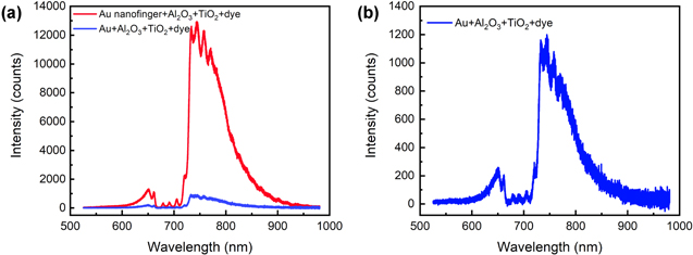
In order to further verify plasmon induced DSSCs performance enhancement, we investigate the fluorescence enhancement of N719 dye on the nanofingers because the fluorescence enhancement is a direct evidence for the absorption enhancement in plasmonic DSSCs [37, 52]. In the experiment, the photoluminescence (PL) of the N719 dye on the 2 nm TiO2 film coated Au/Al2O3/Au nanofingers which is the same as the photoanode of plasmonic DSSCs, and the Au/Al2O3/TiO2 films on the plain glass are measured, as shown in figure 4. The emission peak position of N719 dye almost does not shift and only the fluorescence intensity increases. The results show that the PL enhancement of N719 dye on the plasmonic nanofingers is nearly 10 times higher than the normal photoanode, which is the main reason for the strong plasmonic EM field enhancement. In addition, the LSPR position is only partially overlapped with the emission peak position of N719 dye. By the optimization between the plasmonic resonance and the emission band of dyes, the efficiency of DSSCs can be further improved.
Figure 4. Fluorescence enhancement of N719 dye on the photoanode. (a) Fluorescence intensity of N719 dyes on TiO2–Au/Al2O3/Au nanofingers (red line), and Au/Al2O3/TiO2 composite films (blue line). (b) Magnified view of fluorescence intensity of N719 dyes on Au/Al2O3/TiO2 composite films.
Download figure:
Standard image High-resolution image
4. Conclusions
In summary, we have demonstrated the plasmon enhanced DSSCs through coupled nanofingers. In plasmonic DSSCs, considering the local field enhancement and dye quenching which is both dependent on the separation distance, the collapsed Au/Al2O3/Au nanofingers with 5 nm Al2O3 gap are deposited with 2 nm TiO2 as photoanode to enhance the absorption of sunlight. The results show that, for our designed plasmonic DSSCs, the PCE can be mostly improved, and the maximum power output enhances from 2.7 to 6.5 μW as compared to that based on the photoanode of Au/Al2O3/TiO2 films. The improvement of plasmonic DSSCs performance can be ascribed to the coupled EM field enhancement within the sub-nanometer gap. In addition, fluorescence enhancement of N719 dyes on the plasmonic nanofingers is measured with nearly 10 times higher than that on the plain Au films, which further proves the strong plasmonic effect on DSSCs performance. This plasmonic nanostructure enables the precise engineering of the gap-plasmon modes and can be successfully fabricated by NIL into large areas with low cost, which has huge potentials to be used as photoanode for other types of solar cells, such as organic solar cells, perovskite solar cells.
Acknowledgments
This work was financially supported by the National Key R&D Program of China (No. 2018YFA0306202), the National Natural Science Foundation of China (Nos. 11574270, 11974015 and 11674166, 91963211). W W acknowledges the support from the NSF (No. CMMI-1635612).
Data availability statement
All data that support the findings of this study are included within the article (and any supplementary files).