

Abstract
The averaged power conversion efficiency of polyelectrolytes (P3CT-Na) based MAPbI3 solar cells can be increased from 14.94% to 17.46% with a wetting method before the spin-coating process of MAPbI3 precursor solutions. The effects of the wetting process on the surface, structural, optical and excitonic properties of MAPbI3 thin films are investigated by using the atomic-force microscopic images, x-ray diffraction patterns, transmittance spectra, photoluminescence spectra and Raman scattering spectra. The experimental results show that the wetting process of MAPbI3 precursor solution on top of the P3CT-Na/ITO/glass substrate can be used to manipulate the molecular packing structure of the P3CT-Na thin film, which determines the formation of MAPbI3 thin films.
Export citation and abstract BibTeX RIS
1. Introduction
Regular-type and inverted-type perovskite thin film solar cells have reached the high power conversion efficiencies (PCEs) of 25.2% [1] and 22.3% [2], respectively. The excellent photovoltaic performance of organic-inorganic perovskite solar cells does not only rely on superior material characteristics [3–7] but also relates to the dipole effect of MA cations assisted carrier transport in the MAPbI3 crystal thin films [8–10]. In regular-type perovskite solar cells, TiO2 nanoparticles thin films can be used as the efficient electron transport layer (ETL) [11–13]. However, a high annealing temperature of 450 ℃ is required for the formation of anatase TiO2 crystal structure, which can effectively dissociate the excitons at the MAPbI3/TiO2 interface. In inverted-type perovskite solar cells, poly(3,4-ehylenedioxythiophene)-poly(styrenesulfonate) (PEDOT:PSS) thin films [14–18], poly(triaryl amine) (PTAA) thin films [19–21] and P3CT based thin films [22–24] have used as the hole transport layer (HTL), which can effectively collect the photo-generated holes from the MAPbI3 thin film and thereby resulting in the high short-circuit current density (JSC). PEDOT:PSS thin films have the high transparency in the visible wavelength range. Therefore, the thicker PEDOT:PSS thin films (40–70 nm) can be used to completely cover the roughed surface of ITO glasses [25], which blocks the photo-electrons from the MAPbI3 thin film to the ITO anode electrode. PTAA thin films are hydrophobic polymer layers [26], which are intrinsically incompatible with the hydrophilic MAPbI3 thin films and thereby results in the higher defect density at the MAPbI3/PTAA interface [27]. P3CT polymers are purplish red organic materials, which are also used as the HTL in the highly efficient MAPbI3 solar cells [22–24]. P3CT-Na, P3CT-K, P3CT-Rb, P3CT-Cs and P3CT-CH3NH2 thin films have been used as the efficient HTL of MAPbI3 solar cells. To avoid the light absorption in the HTL, the thickness of the P3CT-based thin films is about 4 nm [22]. In addition, the functional group and main chain of P3CT based polymers are hydrophilic and hydrophobic, respectively. Conceptually, the molecular packing structure of P3CT-based thin films can strongly influence the formation of MAPbI3 thin films, which dominates the photovoltaic performance. To increase the wettability of MAPbI3 precursor solutions on top of the P3CT based thin films, dimethylformamide:dimethyl sulfoxide (DMF:DMSO) (9:1, v/v) solvent mixture is used to dissolve the MAI and PbI2 powders. It means that there is a time-dependent wetting behavior which influences the formation of MAPbI3 thin film and the contact quality at the MAPbI3/P3CT-Na interface. In other words, the contact quality at the MAPbI3/P3CT-Na interface can be improved with an optimized wetting process and thereby increasing the photovoltaic performance of the resultant MAPbI3 solar cells. In this study, the main aim is to investigate the effects of a simple wetting method before the spin-coating process of the MAPbI3 precursor solution on the photovoltaic performance of the resultant solar cells. To the best of our knowledge, this is the first time to investigate the wetting effects of the MAPbI3 precursor solution on top of the P3CT-Na/ITO/glass samples.
2. Experiments
P3CT-Na solution was prepared through the reaction of poly[3-(4-carboxylbutyl)thiophene] (P3CT) (Rieke, America) with sodium hydroxide (99.99%, Alfa Aesar). 9 mg P3CT and 1.975 mg NaOH are dissolved in 4.5 ml deionized (DI) water and 0.9875 ml DI water, respectively. The NaOH/DI water solution is slowly added into the P3CT/DI water solution. Then, the P3CT reacted with NaOH in DI water with stirring at 400 rpm for 9 h at 60 ℃. CH3NH3PbI3 (MAPbI3) precursors were prepared by dissolving MAI crystals (238.4 mg) and PbI2 brown powders (691.5 mg) in a 1 ml DMF:DMSO mixture (9:1, v/v), which resulted in a 1.5 M MAPbI3 precursor solution. 10 mg PCBM powder (99.5%, UR) was dissolved in a 0.5 ml chlorobenzene (CB) (99.8%, Sigma-Aldrich). 1 mg bathocuproine (BCP) powder (99%, Seedchem) was dissolved in a 2 ml isopropanol (IPA) (99.5, ACROS). The perovskite precursor solution, PCBM/CB solution (2 wt%) and BCP/IPA (0.05 wt%) solutions were stirred at 400 rpm for 3 h under room temperatures.
In the device fabrication, the patterned ITO/glass (7 Ω/sq) samples were treated by using a UV-Ozone cleaner for 50 min. Before the deposition of the P3CT-Na thin films, the ITO/glass samples were heated at 140℃ for 10 min in order to remove the residual moisture on the substrates. Then, the 4 nm thick P3CT-Na thin films [22] were spin-coated on top of the ITO/glass samples with a post thermal annealing at 140℃ for 30 min, which can be used as the HTL. The MAPbI3 thin films were fabricated on top of the P3CT-Na/ITO/glass samples by using the one-step spin-coating method with an antisolvent treatment of CB [22–24, 28]. Toluene, iodobenzene and diethyl ether also can be used as the antisolvent [29–31]. Before the spin-coating deposition of the MAPbI3 precursor solution, a simple wetting process is used for 0, 3, 5 and 7 s. The 50 nm thick [6,6]-phenyl-C61-butyric acid methyl ester (PCBM) thin films were spin-coated on top of the MAPbI3/P3CT-Na/ITO/glass samples to act as the ETL. The samples (PCBM/MAPbI3/P3CT-Na/ITO/glass) were modified with a BCP/IPA solution treatment. Finally, the 100 nm Ag cathode electrodes were thermally deposited on top of the PCBM/MAPbI3/P3CT-Na /ITO/glass samples. The active area of the MAPbI3 solar cells is defined to be 0.2 × 0.5 cm2 with the use of a metallic shadow mask during the thermal evaporation process of Ag thin film. The device structure of the P3CT-Na based MAPbI3 solar cell is plotted in figure 1. The J−V curves of the MAPbI3 solar cells were measured in atmospheric environment by using a source-meter system (NI-USB 6356 DAQ) under one sun illumination (AM1.5 G, 100 mW cm−2). The light intensity of the light-emitting diodes based solar simulator (VeraSol-2, newport) was calibrated by using a reference cell (91150 V, newport).

Figure 1. J−V curves of the P3CT-Na based MAPbI3 solar cells with the different wetting times under one sun illumination (AM 1.5 G, 100 mW cm−2). Inset shows the device structure of the solar cell.
Download figure:
Standard image High-resolution imageIn the materials characterizations, the transmittance spectra of P3CT-Na/glass and MAPbI3/P3CT/ITO/glass samples were measured by using a home-made transmittance spectrometer. A broadband lamp light (SL S301, Thorlabs) and a mini optical spectrometer (Mars TB3000+, GIE) were used as the excitation source and detector, respectively. The surface morphologies, crystal structures, photoluminescence (PL) spectra and Raman scattering spectra of the MAPbI3/P3CT-Na/ITO/glass samples were measured by using the atomic-force microscope (AFM) (Innova, Veeco), x-ray diffractometer (XRD) (D8 ADVNCE Eco, Bruker), home-made optical microscope-based PL spectrometer [18] and commercial Raman scattering spectrometer (iHR550, Horiba), respectively. The laser intensities of the PL and Raman measurements are 0.64 W μm−2 and 0.19 mW μm−2, respectively.
3. Results and discussion
Figure 1 presents the light current density−voltage (JV) curves of the P3CT-Na based MAPbI3 solar cells with the different wetting times (WTs) from 0 to 7 s. The averaged photovoltaic performance of 12 solar cells for each condition is listed in table 1. When the WT is 0, the obtained photovoltaic performance is similar to the experimental results in literatures [22]. The PCE can be significantly improved from 14.94% to 17.46% when the WT is 3 s. The PCE decreases from 17.46% to 16.24% with the increase in the WT from 3 to 7 s. Besides, the trends of the series resistance values and shunt resistance values are consistent with the trend of the FF values. The higher shunt resistance (lower series resistance) results in the larger FF. It means that the wetting process mainly influences the contact quality at MAPbI3/P3CT-Na interface. Conceptually, the P3CT-Na thin films can be slightly dissolved by the DMF:DMSO solvent mixture used in the MAPbI3 precursor solution. It can be expected to modify the molecular packing structure of P3CT-Na thin film with a DMF:DMSO solvent mixture treatment. Figure 2(a) presents the absorbance spectra of P3CT-Na/glass samples without and with the DMF:DMSO solvent mixture treatment process. The Urbach energy of the as-prepared P3CT-Na thin film is about 53.7 meV, as shown in figure 2(b). The low Urbach energy also shows that the P3CT-Na is a rigid aromatic polymer [32], which has an intrinsically high hole mobility and thereby results in the efficient exciton dissociation at the MAPbI3/P3CT-Na interface [33]. When the DMF:DMSO solvent treatment is used, the Urbach energy values of the modified P3CT-Na thin films are higher than that of the as-prepared P3CT-Na thin film. It means that the DMF:DMSO solvent treatment can influence the molecular packing structure of the P3CT-Na thin films. The trend of the Urbach energy values (see figure 2(b)) is inversely proportional to the trend of the PCE (see table 1).
Table 1. Photovoltaic performance of the MAPbI3 solar cells under one sun illumination (AM 1.5 G, 100 mW cm−2). The photovoltaic performance data were obtained from 12 cells for each condition.
| Wetting time (s) | VOC (V) | JSC (mA cm−2) | FF (%) | PCE (%) | Rs (Ω) | Rsh (Ω) |
|---|---|---|---|---|---|---|
| 0 | 0.95 ± 0.01 | 23.02 ± 0.58 | 68.3 ± 2.1 | 14.94 ± 0.99 | 44 | 4.1 |
| 3 | 0.96 ± 0.01 | 22.93 ± 0.12 | 79.3 ± 1.1 | 17.46 ± 0.51 | 34 | 24.6 |
| 5 | 0.97 ± 0.01 | 22.03 ± 0.15 | 76.0 ± 1.3 | 16.24 ± 0.56 | 41 | 16.2 |
| 7 | 0.99 ± 0.01 | 21.43 ± 0.16 | 72.1 ± 1.4 | 15.29 ± 0.57 | 46 | 9.3 |
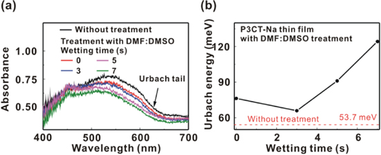
Figure 2. (a) Absorbance spectra of the P3CT-Na/glass samples. (b) Urbach energy values of the P3CT-Na thin films with the different wetting times from 0 to 7 s.
Download figure:
Standard image High-resolution imageFigure 3(a) presents the XRD patterns of the MAPbI3/P3CT-Na/ITO/glass samples with the different WTs from 0 to 7 s, which show that the MAPbI3 thin films are tetragonal structure [30]. The XRD peaks of P3CT-Na thin film and ITO thin film does not detected, which is mainly due to the thick crystalline MAPbI3 thin film (488 ± 18 nm). Figure 3(b) presents the two main XRD peaks at (110) and (220), which can be used to confirm that the MAPbI3 crystal is a body-centered tetragonal structure [34]. Figure 3(c) presents the XRD positions at (110) and the related full-width at half-maximum (FWHM) values of the MAPbI3 thin film with the different WTs. Figure 3(d) presents the XRD intensity ratio of peak at (110) and peak at (220), which can be used to evaluate the lattice distortion of the MAPbI3 crystal. In general, the higher XRD intensity ratio corresponds to the smaller lattice distortion. When the WT is 3 s, the XRD intensity ratio and FWHM have the lowest values, which can be used to evaluate the crystallinity of the resultant MAPbI3 thin films. Besides, the trend of the crystallinities (XRD intensity ratio and FWHM) of the MAPbI3 thin films is inversely proportional to the trend of the Urbach energy values of the P3CT-Na thin films. It means that an appropriate wetting process can decrease the defect densities in the MAPbI3 thin film and P3CT-Na thin film simultaneously.
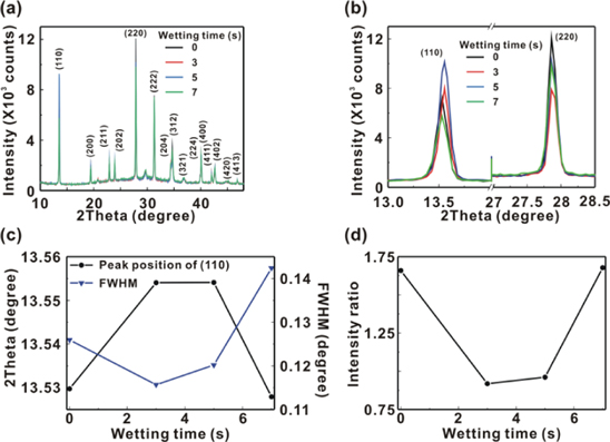
Figure 3. (a) X-ray diffraction (XRD) patterns of the MAPbI3/P3CT-Na/ITO/glass samples; (b) main XRD peaks at (110) and (220); (c) peak position and full-width at half-maximum (FWHM) of (110); (d) peak intensity ratio of (220) and (110).
Download figure:
Standard image High-resolution imageFigure 4 presents the AFM images of the MAPbI3/P3CT-Na/ITO/glass samples with the different WTs from 0 s to 7 s. The surface roughness (Ra) of the MAPbI3 thin film is 17.5 nm when the WT is 0 s, which is due to the co-existences of circle-like and line-like morphologies (see figure 4(a)). The size of the circle-like particles increases with the increase in the WT from 0 to 7 s, which indicates that the wetting process can decrease the number of MAPbI3 nucleation site and thereby increasing the grain size. The closely-packed MAPbI3 thin films can be formed when the WT is 3 s and 5 s, which results in the relatively low surface roughness of 8.03 nm and 8.13 nm, respectively. In other words, the smaller grain size results in the lower surface roughness of the multi-crystalline MAPbI3 thin films [35]. The relatively roughened MAPbI3 thin film can be formed (see figure 4(d)) when the WT is 7 s. The roughened MAPbI3 thin film cannot be completely covered with a 50 nm thick PCBM thin film, which can be used to explain the decrease in the FF from 79.3% to 72.1% with the increase in the WT from 3 to 7 s. (see table 1). Figure 5 presents the transmittance spectra of the MAPbI3/P3CT-Na/ITO/glass samples with the different WTs from 0 to 7 s. The amplitudes of the interference ripples in the transparent wavelength range are related to the Ra values of the MAPbI3 thin film (see figure 4). The lower Ra value results in the larger amplitude of the interference ripples [36, 37]. Besides, the transmittance spectra in the absorption band are almost the same, which indicates that the light harvesting ability of the resultant MAPbI3 thin films is not significantly influenced by the different WT (surface morphology).

Figure 4. Atomic-force microscopic images of the MAPbI3/P3CT-Na/ITO/glass samples with the different wetting times: (a) 0 s, (b) 3 s, (c) 5 s and (d) 7 s.
Download figure:
Standard image High-resolution image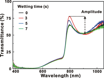
Figure 5. Transmittance spectra of the MAPbI3/P3CT-Na/ITO/glass samples with the different times from 0 to 7 s.
Download figure:
Standard image High-resolution imageFigure 6(a) presents the PL spectra of the MAPbI3/P3CT-Na/ITO/glass samples with the different WTs from 0 to 7 s. The PL peak intensity decreases with the increase in the WT from 0 to 7 s, which can be used to evaluate the crystallinity (defect density) of the MAPbI3 thin film and the contact quality at the MAPbI3/P3CT-Na interface. The lower PL intensity corresponds to the formation of lower crystallinity MAPbI3 thin film and/or the better contact quality at the MAPbI3/P3CT-Na interface, which is consistent with the concept of wetting process. In the top-side excitation, the photo-generated excitons in the MAPbI3 thin film can be mainly trapped by the surface defects before the exciton (carrier) diffusion to the MAPbI3/P3CT-Na interface. In other words, the higher PL intensity from the top region of the MAPbI3 thin film corresponds to the higher JSC (see table 1) because the residual excitons can be efficiently dissociated at the PCBM/MAPbI3 interface [38]. Figure 6(b) presents the peak wavelength and FWHM values in the PL spectra of the MAPbI3/P3CT-Na/ITO/glass samples. The trend of the FWHM values in the PL spectra is inversely proportional to the trend of the FWHM values in the XRD peak at (110), which means that the MAPbI3 particles are merged grains [35]. Besides, the trend of the peak wavelength in the PL spectra is inversely proportional to the trend of peak position in the XRD patterns. The shorter peak wavelength originates from the smaller lattice constant (larger XRD angle). When the WT is 3 s, the peak wavelength of the PL spectrum and the FWHM of the main XRD of the resultant MAPbI3 thin film are smallest and narrowest, respectively. It means that the closely-packed MAPbI3 thin film can be formed on top of the P3CT-Na/ITO/glass sample when the WT is 3 s, which is consistent with the AFM images (see figure 4). Figure 7 presents the PL spectra from the MAPbI3/P3CT-Na interface by using a bottom excitation method [39, 40]. When the WT is 0 s, the PL intensities are highly related to the measured positions, which mean that the contact quality at the MAPbI3/P3CT-Na interface is not uniform. When the WT is 3 s, the PL uniformity is better, which can be used to confirm that the contact quality at the MAPbI3/P3CT-Na interface can be increased with the wetting process. Besides, the standard deviation of the PL width is 3.37 nm (0.37 nm) when the WT is 0 s (3 s), which also indicates that the contact quality at the MAPbI3/P3CT-Na interface can be increased with a WT of 3 s.

Figure 6. (a) PL spectra of the MAPbI3/P3CT-Na/ITO/glass samples under the top excitation. (b) Peak wavelengths and full-width at half-maximum (FWHM) values of the PL spectra.
Download figure:
Standard image High-resolution image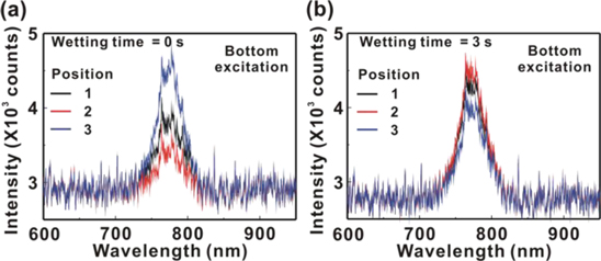
Figure 7. PL spectra of the MAPbI3/P3CT-Na/ITO/glass samples with the different wetting times (WT) under the bottom excitation. (a) WT = 0 s; (b) WT = 3 s.
Download figure:
Standard image High-resolution imageFigure 8 presents the Raman scattering spectra of the MAPbI3/P3CT-Na/ITO/glass samples with the different WTs from 0 to 7 s. There are three peaks which can be assigned to the PbI mode, MA liberation mode and MA torsion mode, respectively [9, 41]. In the lowest Raman shift band from 55 to 100 cm−1, the PbI stretching mode and PbI bending mode are merged together. Figure 9 presents that the Raman intensities (FWHM values) of the PbI mode and MA liberation mode have the highest (lowest) values when the WT is 3 s. The trend of the Raman scattering spectra is consistent with the trends of the XRD patterns (see figure 3) and PL spectra (see figure 6). Besides, the P3CT-Na thin film has the lowest Urbach energy when the WT is 3 s. Therefore, it can be concluded that the more ordered molecular packing structure in the P3CT-Na thin film induces the formation of higher crystalline MAPbI3 thin film, which results in a better contact quality between the hydrophilic MAPbI3 thin film and the hydrophobic P3CT-Na thin film. It can be understood that the hydrophilic group of Na+ in the P3CT-Na thin film plays an important role during the formation of the hydrophilic MAPbI3 thin films.
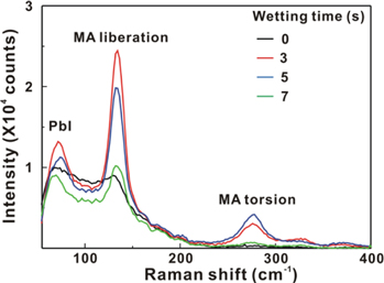
Figure 8. Raman scattering spectra of the MAPbI3/P3CT-Na/ITO/glass samples with the different wetting times from 0 to 7 s.
Download figure:
Standard image High-resolution image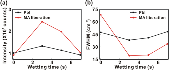
Figure 9. (a) Raman peak intensities of PbI and MA liberation modes. (b) Full-width at half-maximum (FWHM) values of Raman scattering peaks at PbI and MA liberation modes.
Download figure:
Standard image High-resolution image
The PCE of the P3CT-Na based MAPbI3 solar cells is proportional to the FF (see table 1). When the WT of the MAPbI3 precursor solution on top of the P3CT-Na/glass sample increases from 0 s to 3 s, the molecular packing structure of P3CT-Na thin film (see figure 2(b)), the crystallinity of MAPbI3 thin film (see figure 3) and the contact quality at MAPbI3/P3CT-Na interface (see figure 7) both are improved due to solvent treatment effects [42]. It can be used to explain the significant improvement of FF from 68.3% to 79.3% when the WT increases from 0 to 3 s. When the WT increases from 3 to 7 s, the FF decreases from 79.3% to 72.1%, which is mainly due to the increase in the surface roughness of the MAPbI3 thin film from 8.03 to 11.40 nm. It can be explained that the roughened MAPbI3 thin film cannot be completely covered with a 50 nm thick PCBM thin film [35], which can result in the direct contact between Ag and MAPbI3 and thereby forming carrier recombination centers (Ag atoms) at the PCBM/MAPbI3 interface.
4. Conclusions
In summary, we have fabricated the P3CT-Na based MAPbI3 solar cells, which results in the highly averaged PCE of 17.46%. The absorbance spectra of the P3CT-Na/glass samples and the photoluminescence peak intensities of the MAPbI3/P3CT-Na/ITO glass samples show that the contact quality at the MAPbI3/P3CT-Na interface can be increased by increasing the WT. Besides, the molecular packing structure of the P3CT-Na can be varied during the wetting process of DMF:DMSO (9:1, v/v) solvent mixture. When the WT is 3 s, the closely-packed crystalline MAPbI3 thin film can be formed on top of the P3CT-Na/ITO/glass sample and thereby resulting in the best photovoltaic performance.
Acknowledgments
This work was supported by the Ministry of Science and Technology under Grant MOST 107-2112-M-033-001-MY3.
Data availability statement
All data that support the findings of this study are included within the article (and any supplementary files).