

Abstract
InGaN nanostructures are among the most promising candidates for visible solid-state lighting and renewable energy sources. To date, there is still a lack of information about the influence of the growth conditions on the physical properties of these nanostructures. Here, we extend the study of InGaN nanowires growth directly on Si substrates by plasma-assisted molecular beam epitaxy. The results of the study showed that under appropriate growth conditions a change in the growth temperature of just 10 °C leads to a significant change in the structural and optical properties of the nanowires. InGaN nanowires with the areas containing 4%–10% of In with increasing tendency towards the top are formed at the growth temperature of 665 °C, while at the growth temperatures range of 655 °C–660 °C the spontaneously core–shell NWs are typically presented. In the latter case, the In contents in the core and the shell are about an order of magnitude different (e.g. 35% and 4% for 655 °C, respectively). The photoluminescence study of the NWs demonstrates a shift in the spectra from blue to orange in accordance with an increase of In content. Based on these results, a novel approach to the monolithic growth of InxGa1−xN NWs with multi-colour light emission on Si substrates by setting a temperature gradient over the substrate surface is proposed.
Export citation and abstract BibTeX RIS
1. Introduction
Ternary Inx Ga1−x N compounds are of particular interest for applications in solid-state lighting [1] and renewable energy sources [2, 3] due to the ability of light emission tuning from near UV to near IR. However, enormous lattice constants mismatch between InN and GaN (10.7% and 15.0% for a and c constants, respectively) results in the miscibility gap in Inx Ga1−x N layers with xIn = 0.2–0.8 at the usual growth temperature [4–6]. As a consequence, the growth of InGaN layers is often accompanied by the segregation of InGaN clusters with Ga-rich and In-rich regions. Besides, the growth of high crystalline quality InGaN layers is complicated by the lack of lattice-matched substrates. One of the possible ways to overcome these difficulties is the growth of the nanowires (NWs). It has been demonstrated that the elastic strain relaxation on the nanowire sidewalls can help to overcome the InGaN miscibility gap and achieve a better band-gap tunability than in a bulk alloy [6–8]. Another advantage of the elastic strain relaxation on the nanowire sidewalls is the possibility of growth of practically defect-free NWs on substrates with different lattice constants and different thermal expansion coefficients [9, 10]. In this regard, the growth of NWs on silicon substrates is one the most promising approach from the point of view of wide applications and low cost.
Over the past decade, phosphor-free white- or multi-colour light emitting diodes (LEDs) based on InGaN/GaN have been attractive object, since they can overcome the drawbacks of common phosphor LEDs such as stokes energy conversion loss and reduced thermal stability of phosphor [11–13]. The growth of multiple InGaN quantum wells (QWs) or disks (QDs) with various In content in GaN NWs is currently prevalent in a significant number of publications [11, 14–23]. However, it is difficult to obtain uniform carrier injection into stacked QWs or QDs under electrical pumping [24, 25]. In addition, polarization fields of InGaN QWs with high In content grown on polar planes induce a very low overlap of electron-hole wave functions (about 1% in polar InGaN/GaN QWs) decreasing the total internal quantum efficiency [26, 27]. In contrast, the growth of InGaN NWs can contribute to overcome these challenges and to obtain a homogeneous alloy with high In content. To date, most of the InGaN NWs on Si have been elaborated by metal-organic chemical vapor deposition [7, 8, 28, 29] or by molecular beam epitaxy (MBE), but via GaN seeds as the first step [30–38]. To the best of our knowledge, the direct growth of InGaN NWs on Si using MBE is presented by only a few groups [39–42] and there is still a lack of information on the growth conditions influence on physical properties of these nanostructures.
Here, we extend the study of InGaN nanowires growth directly on Si substrates by plasma-assisted MBE A change in the growth temperature of just ∼10 °C leads to a significant change in structural properties of nanowires and shifts the photoluminescence emission from orange to blue. A novel approach to monolithic growth of Inx Ga1−x N NWs exhibiting multi-colour light emission on Si substrate is proposed.
2. Materials and methods
The InGaN nanostructures were grown directly on p-type Si(111) substrates using Riber Compact 12 MBE setup, equipped with Ga, In effusion cells, and a nitrogen plasma source. Initially, the substrate was treated by the Shiraki method [43], then it was transferred to the growth chamber and heated to 950 °С to remove silicon oxide. After the thermal treatment, an atomically clean Si surface was obtained as confirmed by the RHEED observation of a 7 × 7 surface reconstruction. Afterwards, the substrate temperature was decreased to the desired value allowing the growth of InGaN nanostructures. After the stabilization of the substrate temperature, the nitrogen plasma source was ignited at 450 W power, and the N flux was set to 0.4 sccm. At this moment, the growth chamber pressure was 7.4 · 10−6 Torr. Finally, In and Ga effusion cells were simultaneously opened and the InGaN structures were grown during 20 h. The fluxes of In and Ga, measured by Bayard-Alpert vacuum gauge before the growth, were constant throughout the experiment, equal to each other, and amounted to 1 · 10−7 Torr. The growth was performed under N-rich conditions. The appearance of a spotty RHEED pattern corresponding to the formation of three-dimensional crystals with hexagonal crystallographic phase was detected after 120 s of the growth. We carried out several growth experiments at various substrates temperatures, varying from 655 °C to 665 °C.
The morphology of the samples was studied by scanning electron microscopy (SEM supra 25 Zeiss). Photoluminescence (PL) of the samples was excited with a helium–cadmium (He−Cd) metal-vapor laser with a wavelength of 325 nm at 15.5 mW. The PL signal was detected using a DK480 Spectral products monochromator and a single-channel silicon detector using synchronous detection (SRS 510 'stanford research systems'). The measurements were performed at room temperature. The microstructure and chemical composition of grown structures were investigated by high-angle annular dark-field scanning transmission electron microscopy (HAADF-STEM, JeolJEM-2100FTEM) with energy-dispersive x-ray (EDX) spectroscopy techniques (XFlash 6TI30, Bruker).
3. Results and discussion
Figure 1 shows typical SEM images of the InGaN NWs grown at different substrate temperatures: (a) sample A which was grown at 665 °C, (b) sample B grown at 660 °C, (c) sample C grown at 655 °C.
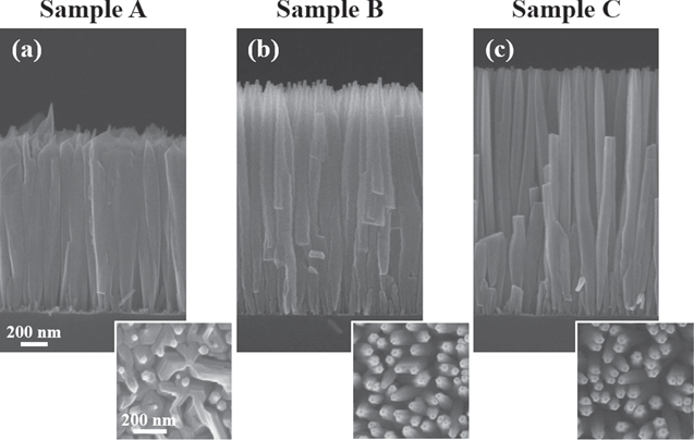
Figure 1. Typical cross-section SEM images of the InGaN NWs grown on Si(111) substrates at various substrate temperatures: (a) sample A grown at 665 °C; (b) sample B grown at 660 °C; (c) sample C grown at 655 °C. The insertions show plan-view SEM images of the corresponding samples.
Download figure:
Standard image High-resolution imageAs can be seen from figure 1(a), sample A consists of coalesced NWs with an average height of 1.3 μm. The NWs diameter is not constant and increases from 20–30 nm at the substrate surface to 200 nm at the middle, up to the coalescence of the NWs sidewalls. At the top of the structure, the NWs diameter decreases to 15–25 nm. Figure 1(b) and corresponding insert below demonstrate the surface morphology of sample B. It is clearly seen that the structure contains both separated and partially coalesced NWs with an average height of about 1.65 μm. The NWs diameter is predominantly 100–150 nm and significantly decreases to 20–30 nm at the top. With a further decrease of the substrate temperature to 655 °C, the separated NWs are mainly formed. Their average height is 1.85 μm and the diameter is 100–120 nm at the middle, 50–60 nm at the top (sample C, SEM image of which is shown in figure 1(c) and the corresponding insert).
In table 1, we have summarized the morphological parameters of the samples. As can be seen from the table, with the substrate temperature decrease the average NWs height increases, the average lateral size of a single NW decreases at the middle, and, conversely, increases at the top. These changes in the morphological parameters are partly explained by an increase in the number of embedded In atoms in the NWs during the growth at decreased substrate temperature, as will be shown below.
Table 1. Morphological parameters of InGaN NWs grown at different substrate temperatures.
| Parameter | Substrate temperature, °C | Average height of NWs, μm | Average lateral size of single NWs, nm | ||
|---|---|---|---|---|---|
| bottom | middle | top | |||
| Sample A | 665 | 1,3 | 20–30 | 200 | 15–25 |
| Sample B | 660 | 1,65 | 20–30 | 120–150 | 20–30 |
| Sample C | 655 | 1,85 | 20–30 | 80–120 | 30–40 |
To study the NWs by TEM, a part of coalesced NWs and single NWs were detached from the silicon substrates and transferred on the TEM grids.
Figure 2 shows HAADF-STEM and EDX images of InGaN NWs grown at 665 °C (sample A). As can be seen from the figure, the NWs chemical composition is irregularly distributed. The In content increases from the bottom to the top within the NW and accumulates near the top. The EDX spectrum in figure 2(d) indicates that at the top of the NWs xIn is about 10%. Taking into account that the growth was carried out at the In/Ga beam equivalent pressure ratio of 1, we can conclude that the In atoms had a lower sticking coefficient in comparison to the Ga atoms.

Figure 2. (a) HAADF-STEM images of an InGaN NWs (sample A); (b) high-resolution elemental mapping of the Ga intensity along the NW; (c) high-resolution elemental mapping of the In intensity along the NW; (d) the EDX spectrum of the NW top.
Download figure:
Standard image High-resolution imageFigure 3 demonstrates the HAADF-STEM images and typical EDX spectrum of a non-coalesced part of an InGaN NW of sample C. It should be noted that sample B has a structure, similar to sample C. In this regard, further discussion of the TEM study will refer to samples B and C simultaneously.
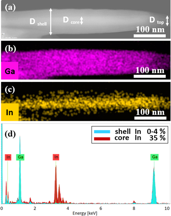
Figure 3. (a) HAADF-STEM images of a non-coalesced part of an InGaN NW (sample C); (b) high-resolution elemental mapping of the Ga intensity along the NW; (c) high-resolution elemental mapping of the In intensity along the NW; (d) typical EDX spectrum of the NW top for the core and shell.
Download figure:
Standard image High-resolution imageLet us discuss the data which can be extracted from HAADF-STEM images (see figures 3(a)–(c)) and compare them with the data from figure 2. The internal structure of the sample B and C differs significantly from that of the sample A. Main difference is the formation of pronounced core–shell structure inside non-coalesced NWs, which is clearly seen in figure 3(a). The core diameter (Dcore) is 25 nm and is constant along the NW, while the Dshell is thinned to the top. Figures 3(b), (c) shows the elemental mapping of Ga and In intensities. According to the elemental contrast, the In atoms are mainly located inside the NW core. The EDX spectrum of the NW shown on figure 3(c) demonstrates In content of about 35% inside the core and 0%–4% inside the shell. As for sample B, In content in the NWs inside the core and the shell is about 30% and 0%–4%, respectively. It is worth noting that the NWs from the bottom to the top exhibit a pure wurtzite crystal structure.
Figure 4 shows room temperature photoluminescence (RT PL) spectra of grown samples. The insert of figure 4 demonstrates room temperature luminescence of samples A, B, and C visible to the naked eye under optical pumping by a defocused laser beam.

Figure 4. Typical RT PL spectra of the InGaN NWs grown at various substrate temperatures. The insert shows the luminescence of the samples visible to the naked eye.
Download figure:
Standard image High-resolution imageSample A exhibits a broad PL spectrum from 380 to 550 nm with a maximum at about 428 nm. An asymmetric shape of the spectrum with several emission lines in the long-wavelength region is observed and can be explained by the formation of InGaN different solid solutions with inhomogeneous chemical composition in accordance with the TEM results. The total volume of the In-rich areas is rather small in comparison with those having smaller In content. That is why we may expect intensive signal in the short-wavelength region corresponding to the low In content area. Compared to sample A, the PL spectra of the samples B and C show similar intensities with maxima in the long-wavelength region at 518 and 566 nm, respectively. In addition, the weak intensity bands in the short-wavelength range of 380–430 nm are detected. Let us analyze the spectra of the samples B and C in more detail. The most intense signals are attributed to the NWs core, while the weak intensity bands are attributed to the NWs shell. It should be noted that the photoluminescence of the InGaN shell has not been previously documented. The full width at half maxima of the samples B and C are 72 and 76 nm, respectively, which are explained by the In content fluctuation within the NWs core. A tentative In content range within the NWs core was estimated ∼7%, which is comparable with the best results for similar structures grown on Si [40] and sapphire substrates [44].
Knowing the chemical composition in the different parts of NWs (core and shell) and the PL peak positions of grown NWs, we have compared our data with the composition dependencies for the relaxed and strained InGaN layers. A modified Vegard's law which includes both linear interpolation and a quadratic term depending on a bowing parameter b was used to plot the composition dependencies. The Eg InN is used as 0.7 eV, Eg GaN is used as 3.43 eV, while b amounts to 2.85 and 1.43 eV for the relaxed and strained InGaN, respectively. The results are shown in figure 5. The orange points are our data, and the composition dependencies (violet and red curves) are plotted using the analysis undertaken in [45].
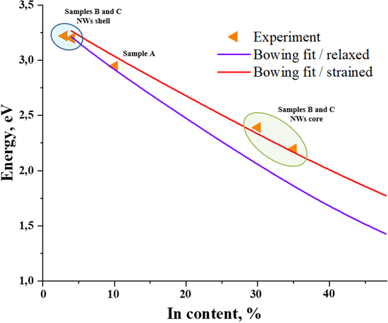
Figure 5. Composition dependencies of the room temperature band-gap. The orange points are the data determined by the EDX and RT PL measurement. The bowing fits are plotted using the analysis undertaken in [45]. The red curve corresponds to strain InGaN layers. The purple curve corresponds to relaxed InGaN layers.
Download figure:
Standard image High-resolution imageAs can be seen from the figure, the positions of the energies for the NWs core (around the In content of 30%–35%) are close to the bowing fit of the strained InGaN, which indicates an existence of strain inside the NWs core. At the same time, the presence of strain in the NWs shell cannot be estimated from the plot, since the energy difference between strained and relaxed InGaN is low for low In content. Thus, the results are in a good agreement with the analysis for low In content given in [45] and experementally prove the existance of strained InGaN inside the NW core with bigger In content.
Taking into account that the miscibility gap is one of the reasons of the low efficiency in the green spectral range (≪green gap≫) [46], the grown samples can possess an undoubted advantage. Based on this, it is potentially possible to realize white or multi-colour emission with high internal quantum efficiency based on the InGaN NWs grown in the narrow range of substrate temperatures from 655 to 665 °С. To demonstrate the possibility of creating multi-colour emitters on these structures, we have designed a special substrate holder that provides a small temperature gradient along the substrate surface (∼10 °C) under a constant substrate heater temperature. Figure 6 shows a RT PL spectrum of the grown sample under optical pumping with a defocused laser beam with an area of 4 mm2. As can be seen from the figure, the spectrum has two pronounced broad emission areas with maxima of 430 and 545 nm. To shed more light into the nature of the whole spectral range, we have performed the analysis of the spectrum via the Voigt function deconvolution showing three different bands. Accordingly, the emission at 430 nm corresponds to the broad photoluminescence area of sample A, while the emission of 545 nm consists of two luminescence bands at 530 and 570 nm corresponding to the samples B and C, respectively.

Figure 6. Typical RT PL spectrum of the InGaN NWs monolithically grown by a special substrate holder on a single Si substrate. The deconvolution is shown for guide eyes only.
Download figure:
Standard image High-resolution image
Hence, by setting the temperature gradient along the substrate surface, it is possible to monolithically grow a multi-colour InGaN element within a single run on the same Si substrate.
4. Conclusions
To conclude, we have determined the conditions for the growth Inx Ga1−x N NWs with xIn up to 35% on the Si substrates by plasma-assisted MBE. The SEM and STEM studies demonstrate that, under appropriate growth conditions, a change of the substrate temperature by only 10 °C leads to a significant change in the InGaN structure from an inhomogeneous solid solution to core–shell NWs. The grown InGaN NWs exhibit a strong RT PL in the ≪green gap≫ range that is promising for creating highly efficient LEDs based on these NWs. A novel approach to the growth of InGaN NWs at a small temperature gradient over the substrate surface demonstrates the potential for the implementation of multi-colour light emitters monolithically grown within a single run on the same Si substrate.
Acknowledgments
The samples were grown under support of Ministry of Science and Higher Education of the Russian Federation (state task № 0791-2020-0003). The optical properties were studied under financial support of RSF grant (project № 19-72-30010). TEM studies were conducted using the facilities of the Federal Joint Research Center 'Materials science and characterization in advanced technology'. SEM characterization was done under support of St. Petersburg State University research grant 61520973. NVK gratefully acknowledged support from the Basic Research Program of the National Research University Higher School of Economics.
Data availability statement
All data that support the findings of this study are included within the article (and any supplementary files).
Authors' statement/competing interests
The authors declare no conflict of interest.