

Abstract
Energy conversion to generate hot electrons through the excitation of localized surface plasmon resonance (LSPR) in metallic nanostructures is an emerging strategy in photovoltaics and photocatalytic devices. Important factors for surface plasmon and hot electron generation are the size, shape, and materials of plasmonic metal nanostructures, which affect LSPR excitation, absorbance, and hot electron collection. Here, we fabricated the ordered structure of metal-semiconductor plasmonic nanodiodes using nanosphere lithography and reactive ion etching. Two types of hole-shaped plasmonic nanostructures with the hole diameter of 280 and 115 nm were fabricated on Au/TiO2 Schottky diodes. We show that hot electron flow can be manipulated by changing the size of plasmonic nanostructures on the Schottky diode. We show that the short-circuit photocurrent changes and the incident photon-to-electron conversion efficiency results exhibit the peak shift depending on the structures. These phenomena are explicitly observed with finite difference time domain simulations. The capability of tuning the morphology of plasmonic nanostructure on the Schottky diode can give rise to new possibilities in controlling hot electron generation and developing novel hot-electron-based energy conversion devices.
Export citation and abstract BibTeX RIS
1. Introduction
In recent decades, localized surface plasmon resonance (LSPR), occasioned by nanostructured plasmonic metals, has attracted widespread attention in the application, including as a fundamental element of photocatalytic devices and photovoltaics, significantly increasing their efficiency [1–7]. As the nanostructured plasmonic metal is exposed to a photon, metal-free electrons oscillate with the specific wavelengths of the photon, and LSPR occurs. LSPR excitation either decays radiatively, via re-emitting the photon as near-field coupling and far-field scattering, or non-radiatively, via the generation of a highly energetic electron (1–3 eV). This electron is called the 'hot electron' excited through Landau damping [8, 9] and chemical interface damping [9–11]. The hot electron, however, has a short lifetime of only femtoseconds and should be collected with the Schottky junction between metal and semiconductor; it has high enough energy to overcome the Schottky barrier and is injected into the semiconductor [12–18]. Schottky devices that utilize hot electrons can also make solar devices more efficient [6, 19–29].
The first study on utilizing hot electrons suggested a possible cause for the planar Schottky photodiode combined with dye molecules and Au/TiO2, demonstrated by McFarland and Tang [12]. The dye molecules acted as photosensitizers and a source of hot electrons. Lee et al fabricated plasmonic Au/TiO2 nanodiodes. Hot electron flow, induced by LSPR of Au, was detected as incident photon-to-electron conversion efficiency (IPCE), as well as photocurrent [6]. Further studies showed the boosting of hot electron flow by integrating PbS quantum dots or MAPbI3 perovskite into plasmonic Au/TiO2 nanodiodes [26, 29]. When the plasmonic nanodiode is coupled with other sensitizers, hot electron flow can be enhanced through near field coupling. The enhancement of hot electron flows and their origin are revealed by means of the IPCE measurement.
LSPR excitation and hot electron generation can be manipulated with changes in the size, shape, and materials of the plasmonic structure, tuning the absorption of specific photon wavelengths and hot electron collection. Various studies have been conducted to control LSPR excitation of plasmonic metals with these parameters [30–34]. Plasmonic metals can be synthesized in various shapes and sizes, applying photochemistry and photoelectrochemistry. Unfortunately, plasmonic devices, which can be controlled with the parameters, have been mostly unsuccessful to date, mainly because devices for directly detecting hot electrons should be connected and nanostructured. Random plasmonic structures can be achieved by annealing metal-thin-film on metal/TiO2 nanodiodes [6, 21]. In this case, the size and shape of metal nanostructures were random. Therefore, the IPCE peak position changed slightly each time the Au/TiO2 nanodiodes were fabricated [6, 19, 26, 29]. The random structures of the plasmonic nanodiodes made it difficult to obtain quantitative comparisons to other plasmonic metals, e.g. silver [35, 36], copper [37, 38], and aluminum [39, 40]. Consequently, there remains a need for diode fabrication methods that can be manipulated in size, shape, and materials.
There are a few methods to fabricate nano or meso porous structures for the Schottky nanodiodes, such as plasma electrolytic oxidation and anodization [41–44]. In this study, we used nanosphere lithography with reactive ion etching to fabricate the ordered and connected nanostructure of plasmonic metals. Nanosphere lithography is well known as a facile method for making nanostructures [45–47]. The shape of plasmonic Au can be well-defined, and its size can be controlled depending on etching time. We measured the optical properties of plasmonic Au for the specific shape according to the size difference. This showed that the IPCE peak of the Au/TiO2 nanodiodes can be manipulated with the particular shape and the size difference. Furthermore, to clarify the LSPR phenomenon and hot electron transportation, finite difference time domain (FDTD) simulations were carried out; the simulations demonstrate the theoretical absorbance spectra and the electric field distributions for hot electrons.
2. Experimental section
2.1. Nanodiode fabrication
To briefly explain nanodiodes, plasmonic Au is on top of n-type TiO2 (n-TiO2), and n-TiO2 is on the framework insulator TiO2 (f.i-TiO2), using nanosphere lithography with reactive ion etching. The scheme of the fabrication process of plasmonic Au/TiO2 nanodiodes is illustrated in figure 1. First, polystyrene (PS) beads—from Sigma Aldrich—in the nanopattern of hexagonal close-packing, of which the diameter is 460 nm, were coated on the quartz substrate (10 × 20 mm2) with the self-assembly method of nanosphere lithography [28, 47]. Ethanol dilutes the PS beads solution to 50%. Then, 170 μl of a 2% sodium dodecyl sulfate solution was dropped on the water contained in the petri dish. 5 μl of the PS solution was slowly dropped on a sliding glass laid obliquely in the petri dish, while arranged in a monolayer. The PS beads monolayer on the water surface was lifted off with the quartz substrate. Second, it was etched with oxygen plasma in the reactive ion etching chamber to reduce the size of the PS beads. Third, 90 nm of TiO2 thick film was deposited on the sample through the electron beam evaporator. This TiO2, named f.i-TiO2, acted simply as a framework insulator. This process was prepared with a 3.5 × 6.5 mm2 stainless steel mask and 0.4 Å s−1 deposition rate under a vacuum of 8.5 × 10⁻⁷ Torr. Fourth, the sample was sonicated for 20 min in toluene solution (Sigma Aldrich) to remove PS beads and for 10 min in water to rinse the toluene. Fifth, 100 nm thickness of Ti film was deposited on f.i-TiO2 film using the electron beam evaporator with a 3 × 6 mm2 stainless steel mask and 0.8 Å s−1 deposition rate under the vacuum of 2.0 × 10⁻⁶ Torr. Sixth, the sample was annealed at 400 °C in the air for 3 h to make n-TiO2, named n-TiO2. Seventh, two Au/Ti electrode pads were deposited. The Ti was 50 nm of thick film, and Au was 100 nm of thick film using the electron beam evaporator with a 3 × 6 mm2 stainless steel mask and 1.0 Å s−1 deposition rate under the vacuum of 2.0 × 10⁻⁶ Torr. The Ohmic contact electrode pad was on n-TiO2/f.i-TiO2 film, and another electrode for connecting the Schottky contact was on the quartz. Finally, to build the Schottky junction between plasmonic Au and n-TiO2, 30 nm of thin Au film was deposited on the position between the n-TiO2/f.i-TiO2 film and the Au/Ti electrode pad using the electron beam evaporator with a 0.5 × 10 mm2 stainless steel mask and a deposition rate of 0.5 Å s−1 under the vacuum of 8.5 × 10⁻⁶ Torr. The Schottky junction area of plasmonic Au on n-TiO2 was 0.5 × 0.5 mm2. Therefore, changing the etching time and size of standardized PS beads facilitates control of the hole size.

Figure 1. A fabrication process of plasmonic Au/n-TiO2/f.i-TiO2 nanodiodes.
Download figure:
Standard image High-resolution image2.2. Characterization
The optical and electric properties of the plasmonic nanodiode were carried out as follows: current density–voltage curves and short-circuit photocurrent density curves were measured in air conditions at room temperature using a source meter (Keithley Instrumentation 2400). Current density–voltage curves and short-circuit photocurrent density were obtained with the sweep mode and the ammeter mode, respectively. For the short-circuit photocurrent density of the light source, a tungsten-halogen lamp of 9 mW cm−2 was used perpendicular to the nanodiodes. The spectrum of the lamp is displayed in figure S1 (available online at stacks.iop.org/NANO/32/225203/mmedia). This contains light in the visible region. Lumerical Inc. offers FDTD simulations to characterize absorbance spectra and electric field distribution. IPCE was measured to detect the hot electrons flow from plasmonic Au to n-TiO2 depending on photon energy, with a tunable xenon arc lamp source (Newport, TLS-300XU). Absorbance spectra were measured with the ultraviolet-visible-infrared spectrometer (Shimadzu, UV3600). To characterize them, 1 mm thick quartz plate was used as a substrate of plasmonic Au/TiO2 nanodiodes, and another quartz plate was used as a reference.
3. Results and discussion
3.1. Plasmonic Au/n-TiO2/f.i-TiO2 nanodiodes
Figure 2(a) shows a schematic of hot electron generation on the Au/n-TiO2 Schottky diode under illumination. Hot electron generation is amplified on the side of the hole area, and hot electrons can be transferred to n-TiO2. The energy band diagram of the Schottky junction is shown in figure 2(b). Hot electrons induced by LSPR excitation of plasmonic metals can overcome the Schottky barrier and be found as photocurrent with n-TiO2. Also, hot electrons can be directly transferred with interfacial plasmon decay. Cross-section images of the active area for corrugated hole arrays plasmonic Au/n-TiO2/f.i-TiO2 nanodiodes (CHAP Au/TiO2) fabricated by nanosphere lithography with reactive ion etching are shown in figures 2(c) and (d). The real cross-sectional morphology of corrugated hole arrays is confirmed through scanning transmission electron microscopy, a high-angle annular dark-field image (figure 2(c)), and an elemental mapping image with energy-dispersive x-ray spectroscopy (EDS) (figure 2(d)). When deposited, 30 nm Au thin film could become spontaneously nanostructured as a corrugated structure with the nanostructured framework. Under illumination, LSPR occurs in nanostructured Au, and hot electrons can be generated. These hot electrons are injected into n-TiO2. N-TiO2 is an n-type semiconductor, which has high crystallinity, whereas f.i-TiO2, which is the simple framework, is an insulator and amorphous. Crystallinity information about those TiO2 is shown in x-ray diffraction (figure S2). Bare quartz and f.i-TiO2 do not have x-ray diffraction peaks. N-TiO2 has peaks for anatase and rutile. The nanostructured Au consists of the hole areas that correspond to the pit parts of Au. The 140 nm n-TiO2 thick film is located on the 90 nm f.i-TiO2 thick film, and the 30 nm Au thin film is on top of the n-TiO2 thick film. Au thin film is ordered and securely connected as the nanostructure of corrugated hole arrays. The actual structure of the upper area is a slightly rounded, not vertical shape. Finally, Au thin film is deposited 30 nm on corrugated hole arrays and 20 nm on the side between the upperparts and the pit parts.
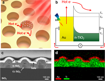
Figure 2. (a) A schematic of hot electron generation on the diode under illumination. (b) Hot electron transport and energy band diagram of Au/n-TiO2. (c), (d) Cross-section images of corrugated hole arrays plasmonic Au/n-TiO2/f.i-TiO2 nanodiodes. (c) Scanning transmission electron microscopy and high-angle annular dark-field image. The hole area corresponds to the pit part of Au. (d) Energy-dispersive x-ray spectroscopy elemental mapping image.
Download figure:
Standard image High-resolution imageTo verify the surface morphology and size of corrugated hole arrays depending on etching time, scanning electron microscope images were taken (figure 3). As etching time increases, the hole diameter decreases. This is because the PS gets smaller during oxygen plasma etching (figure 3(a)). At 60 s etching time, the hole diameter is much larger, and at 150 s, the hole diameter is far shorter. With nanosphere lithography and reactive ion etching, the size of plasmonic Au can be easily controlled. Here, we designate the structure at 60 s etching time as the large-hole-shaped structure (figure 3(b)) and the structure at 150 s etching time as the small-hole-shaped structure (figure 3(c)). The large-hole-shaped structure has 280 ± 2 nm holes, and the gap between the holes is 122 ± 2 nm. The small-hole-shaped structure has 115 ± 4 nm holes, and the gap between the holes is 270 ± 4 nm. To aid in the understanding of the structures, cross-sectional schematics are depicted in figures 3(d) and (e). F.i-TiO2 is deposited in a honeycomb shape between the reduced-sized PS gaps. Then the hole area naturally occurs because n-TiO2 and Au are sequentially deposited. The small PS gaps lead to the large hole area, and the large PS gaps lead to the small hole area.

Figure 3. (a) Schematics of polystyrene (PS) beads. As etching time increases, the size of PS beads decreases. Scanning electron microscope surface images of corrugated hole arrays plasmonic Au/n-TiO2/f.i-TiO2 nanodiodes with the etching time of (b) 60 s and (c) 150 s. Corrugated hole arrays were formed by polystyrene beads size of 460 nm. The structure of 60 s etching is named the large-hole-shaped structure with a large hole diameter; whereas, the structure of 150 s etching is named the small-hole-shaped structure with a small hole diameter. Cross-sectional schematics of (d) the large-hole-shaped structure and (e) the small-hole-shaped structure.
Download figure:
Standard image High-resolution image3.2. Optical properties depending on the hole size
The Schottky junction between plasmonic Au and n-TiO2 is formed, as seen in figure S3. Here, the input bias is on the Schottky electrode, and the output bias is on the Ohmic electrode. When a forward bias is applied, the built-in potential of n-TiO2 becomes flat banding, and electrons of n-TiO2 flow to the plasmonic Au. On the other hand, when a reverse bias is applied, electrons of plasmonic Au cannot move to the n-TiO2 due to the Schottky barrier. This Schottky barrier acts as an energy barrier and electron filter. Therefore, only hot electrons with high energy can cross the Schottky barrier and flow to n-TiO2. In addition, hot electrons can be collected via direct charge transfer. Obtained fitted J–V curves and Schottky barrier heights are also displayed in figure S3(a). The Schottky barrier heights for the large-hole-shaped structure and the small-hole-shaped structure are 0.923 eV and 0.861 eV, respectively. J–V curves in the dark and light are shown in figure S3(b). The Schottky barrier height can be calculated through the fitting of current density–voltage data to the thermionic emission equation [48]:
where A is the active area, A** is the Richardson constant, T is the room temperature, q is the elementary electric charge, kb
is the Boltzman constant,  is the Schottky barrier height,
  is the ideality factor, and Rs
is the series resistance of the nanodiodes.
is the ideality factor, and Rs
is the series resistance of the nanodiodes.
The optical properties of CHAP Au/TiO2 nanodiodes, depending on the hole size, are displayed in figure 4. Figure 4(a) shows the short-circuit photocurrent density with and without illumination. Essentially, the photocurrent density is measured as the reverse current. The photocurrent density values are set to the positive values for convenience. The photocurrent density is enhanced under the light, and plasmon-driven hot electrons occasion this enhancement. For the small-hole-shaped structure, the photocurrent density is higher. Structurally, the hole area of plasmonic Au is surrounded by n-TiO2. The direction of the hot electron momentum corresponds to the direction of the electric field of the incident light. In other words, hot electrons are generated perpendicular to the incident light [13, 26], and the momentum of hot electrons generated in the hole area is directly towards n-TiO2. Accordingly, the hole area collects many hot electrons, and hot electron collection depends on the size of the hole area. Also, in general, the smaller the plasmonic metal, the more plasmonic decay occurs via absorption [5, 49, 50]; therefore, the structure with the small hole area exhibits higher hot electron collection efficiency. Figure 4(b) presents the IPCE spectra of CHAP Au/TiO2 nanodiodes depending on the hole size. Hot electrons are actively generated from 1.8 eV to 2.6 eV of photon energy as a peak in the IPCE spectrum. This can be assigned to the intraband excitation of hot electrons from the sp band of plasmonic Au. The generation of hot electrons between 2.8 eV and 3.2 eV is assigned to the interband excitation of hot electrons from the d band of plasmonic Au. Above 3.2 eV, IPCE increases dramatically because band-to-band excitation in n-TiO2 arises. Each intensity of IPCE depending on the hole size accords with a trend of the photocurrent density. The point here is that the IPCE peak can be manipulated depending on the hole size. The large-hole-shaped structure has a red-shifted IPCE peak (2.2 eV). Whereas, the small-hole-shaped structure has a blue-shifted IPCE peak (2.3 eV). In general, the smaller the size of plasmonic nanostructures, the plasmonic excitation peaks tend to be shifted to the blue [30, 37, 39]. As described above, the hot electron collection of CHAP Au/TiO2 nanodiodes depends on the size of the hole area. Therefore, the IPCE peak of the small-hole-shaped structure is shifted to the blue, and the IPCE peak of the large-hole-shaped structure is shifted to the red. Figures 4(c) and (d) show the absorbance spectra of experimental data and simulated data from FDTD analysis, depending on the hole size. We observe a peak of intraband excitation in each spectrum. Like the IPCE spectrum, this peak is shifted along with the size of the hole area and matches the tendency of the IPCE peak well. Both experimental and simulated absorbance have the plasmonic peak at same position and have the same peak position shift tendency. The small-hole-shaped structure has an additional peak of the interband excitation at 2.9 eV of photon energy. This leads to a linear increase in the IPCE spectrum from the interband excitation of the small-hole-shaped structure, and the IPCE intensity of the small-hole-shaped structure in the interband excitation region is much higher than the large-hole-shaped structure. We note that the mechanisms of plasmonic absorbance are different from those of IPCE. Plasmonic absorbance is the concept of light absorbance where free electrons of metal oscillate at a specific wavelength of the incident light, while IPCE represents the spectrum of hot electron generation by plasmonic decay across the Schottky barrier. Hot electrons generated on the surface of plasmonic Au have a very short mean free path of 20–40 nm [51], so a lot of hot electron energy decay occurs before crossing the Schottky barrier. Therefore, the number of hot electrons that can cross the Schottky barrier is further reduced as they move to the interface between Au and n-TiO2. As higher energy photons are incident, higher energy hot electrons are actively generated [52], so even if the energy of the hot electrons collapses due to the short mean free path, the number of hot electrons across the Schottky barrier increases. As a result, IPCE becomes the most active when photon energy higher than the existing LSPR peak is irradiated; thus, the IPCE peak is blue-shifted more than the absorbance peak. However, the important point is that for each spectrum, as the size of the hole area decreases, both the IPCE peak and the absorbance peak become blue-shifted. These absorbance peaks only appear in nanostructures, and thin Au film does not have any plasmonic absorbance peaks (figure S4). As such, the intensity and peak position of optical and electrical properties can be easily manipulated through control of the size with the particular shape.
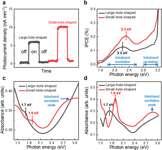
Figure 4. (a)–(d) Optical properties of corrugated hole arrays plasmonic Au/n-TiO2/f.i-TiO2 nanodiodes depending on the hole size. (a) Short-circuit photocurrent density measured with light on-off mode. (b) IPCE as a function of photon energy. The IPCE peak, which means LSPR excitation and hot electron generation, can be shifted with the hole size. (c) Experimental absorbance spectra. (d) Simulated absorbance spectra.
Download figure:
Standard image High-resolution image3.3. Electric field distribution
FDTD electric field distribution was carried out to elucidate LSPR excitation and the hot electron generation of CHAP Au/TiO2 nanodiodes depending on the hole size, and the result is shown in figure 5. The light enters Au/TiO2 perpendicularly, and the electric field distribution images are expressed as Au/TiO2 interfaces in the x−z plane of a cross-section view. The border is represented by the white dotted lines. FDTD simulation models for the electric field distribution were based on the hole size and the photon energy of the absorbance peaks. The main point is to have strong electric field confinement at Au/TiO2 interfaces for efficient collection of hot electrons. Figures 5(a) and (b) are for the large-hole-shaped structure. Under the 1.7 eV photon energy, the peak absorbance position, the strong electric field confinement phenomenon occurs (see inside the yellow circles). On the other hand, the small-hole-shaped structure has much stronger electric field confinement at Au/TiO2 interfaces under the 1.9 eV photon energy, which is the absorbance peak position (figures 5(c) and (d)). Those FDTD electric field distributions, which could also help visualize trends of absorbance and IPCE, were consistent with the peak shift observed on the large-hole-shaped and the small-hole-shaped structures on plasmonic nanodiodes.

Figure 5. FDTD simulation models for electric field distributions at Au/TiO2 interfaces in the x−z plane of the cross-section view. (a) The large-hole-shaped structure under the 1.7 eV photon energy, and (b) under the 1.9 eV photon energy. (c) The small-hole-shaped structure under the 1.7 eV photon energy, and (d) under the 1.9 eV photon energy.
Download figure:
Standard image High-resolution image
Earlier studies of charge separation at plasmonic-semiconductor interfaces have shown strong evidence that the dominant charge transfer mechanism is interfacial plasmon decay (chemical interface damping). Our electromagnetic field enhancement specifically occurs at the interface, further supporting this concept. Overall, the IPCE measurement combined with FDTD simulation indicates that LSPR excitation and hot electron generation can be controlled depending on the hole size. This strategy of changing the morphology of plasmonic nanostructure on the Schottky diode can give rise to the advanced scheme of plasmonic catalysis and photocatalysis due to the ability to control surface plasmon-driven hot electron generation [53, 54].
4. Conclusions
In summary, we fabricated the ordered and connected plasmonic Au structure, from CHAP Au/TiO2 nanodiodes, using nanosphere lithography with reactive ion etching. We show that the nanodiodes for hot electron detection are controllable in size with the specific shape. Varying etching time, the large-hole-shaped structure and the small-hole-shaped structure were fabricated, and both of them exhibit the well-formed Schottky junction between plasmonic Au and n-TiO2. The short-circuit photocurrent density of the small-hole-shaped structure is much higher than the large-hole-shaped structure. Because the hole area of plasmonic Au is geometrically surrounded by n-TiO2, hot electron collection depends on the size of the hole area. Therefore, we conclude that the small-hole-shaped structure can efficiently collect hot electrons. The intensity of the IPCE spectrum of the small-hole-shaped structure is higher for the same reason. Furthermore, the IPCE peak, which means LSPR excitation and hot electron generation, can be manipulated depending on the hole size. As the size of the hole area decreases, the IPCE peak position shifts to the blue. For absorbance spectra, the peak is shifted along with the size of the hole area like the IPCE spectrum. From FDTD electric field distribution, we get the following results: the large-hole-shaped structure amplifies hot electron generation under the 1.7 eV photon energy. Whereas, the small-hole-shaped structure amplifies hot electron generation under the 1.9 eV photon energy. This device allows us to measure the hot electron flux on the well-defined plasmonic Schottky nanodiodes. Above all, this study suggests a novel device in which hot electron flow can be manipulated via the size control of plasmonic nanostructures.
Acknowledgments
This work was supported by the Institute for Basic Science (IBS) [IBS-R004].
Data availability statement
The data that support the findings of this study are available upon reasonable request from the authors.
Conflicts of interest
There are no conflicts to declare.