

Abstract
2D materials offer a pathway for further scaling of CMOS technology. However, for this to become a reality, both n-MOS and p-MOS should be realized, ideally with the same (standard) material. In the specific case of MoS2 field effect transistors (FETs), ambipolar transport is seldom reported, primarily due to the phenomenon of Fermi level pinning (FLP). In this study we identify the possible sources of FLP in MoS2 FETs and resolve them individually. A novel contact transfer technique is used to transfer contacts on top of MoS2 flake devices that results in a significant increase in the hole branch of the transfer characteristics as compared to conventionally fabricated contacts. We hypothesize that the pinning not only comes from the contact-MoS2 interface, but also from the MoS2-substrate interface. We confirm this by shifting to an hBN substrate which leads to a 10 fold increase in the hole current compared to the SiO2 substrate. Furthermore, we analyse MoS2 FETs of different channel thickness on three different substrates, SiO2, hBN and Al2O3, by correlating the p-branch ION/IOFF to the position of oxide defect band in these substrates. FLP from the oxide is reduced in the case of Al2O3 which enables us to observe ambipolar transport in a bilayer MoS2 FET. These results highlight that MoS2 is indeed an ambipolar material, and the absence of ambipolar transport in MoS2 FETs is strongly correlated to its dielectric environment and processing conditions.
Export citation and abstract BibTeX RIS
1. Introduction
Transition metal dichalcogenide (TMDC) based two dimensional (2D) materials have attracted significant attention to be used in both high performance and low power electronics due to their superior properties such as enhanced electrostatic control and non-susceptibility to short channel effects at ultra-scaled dimensions [1, 2]. Molybdenum Disulphide (MoS2) is particularly interesting since it is the most common TMDC that is grown on large area substrates [3, 4] and exhibits excellent electrical characteristics. However, there are several bottlenecks that deter the replacement of current Si based CMOS technology with 2D material based technology. A significant challenge for MoS2 based field effect transistors (FETs), is the inability to fabricate both n-FETs and p-FETs from the same material due to the lack of ambipolar transport. Since 2D materials are affected strongly by their encapsulating environment, there are several factors that play a role in the loss of ambipolarity. One significant reason is the strong Fermi level pinning (FLP) that occurs at the interface between the contact and the MoS2 channel, as widely reported in literature [5–7]. Due to this, the Fermi level of the MoS2 channel (under the contacts) is unable to move freely, resulting in the development of Schottky barriers for charge carrier injection. The Schottky barrier height (SBH) is relatively small for electrons for most contact metals, while for holes it is much larger and independent of the metal used for contacting. The current consensus is that this barrier difference is the reason for the exclusively n-type characteristics observed for MoS2 FETs.
There have been several strategies suggested in other research works to fabricate ambipolar MoS2 FETs, all with their drawbacks in terms of CMOS compatibility. Some of the works aimed to achieve ambipolarity by fabricating a Electric Double layer transistor with ionic gel gating [8, 9]. Although this was the first demonstration of ambipolar transport, there was no significant modulation leading to a poor ON–OFF ratio, in spite of applying a high gate bias. Another work focused on the surface charge transfer mechanisms, to dope the 2D material p-type [10]. Although this work illustrated a gradual transition from n-type to p-type, it uses chemical doping, which could lead to non-uniform results when implemented over large CVD grown MoS2 areas. The use of MoOx contacts as a p-type contact for MoS2 is also a very interesting technique, owing to the work function of MoOx which is around 6.6eV [11], but only leads to ambipolar transport in thick MoS2 flakes (24 nm), which is not interesting for future ultra-scaled CMOS applications. Another research work made use of mechanically delaminated metal pads as contacts to MoS2 flakes [12]. Although this seems promising, the devices are fabricated on a PMMA substrate which again is not CMOS-compatible.
Considering the existing literature, we find inconsistent reports of ambipolar transport in MoS2 FETs and in particular, a lack of understanding with respect to the loss of ambipolarity in MoS2 FETs. Although the mechanism of FLP is generally accepted to be the reason for the loss of ambipolarity, most research works study this effect at the contact interface. In this study, we demonstrate that FLP not only occurs at the contact-MoS2 interface but is also present at the interface between the 2D channel and the underlying substrate, as illustrated in schematic figure 1. We demonstrate for the first time that by inserting an hBN substrate between the MoS2 channel and SiO2 substrate, hole current is boosted by a factor of 10, for the same MoS2 device. We discuss the impact of the defect bands of the substrate on the loss of ambipolar transport, which allows us to select a technologically relevant dielectric, Al2O3, that provides a significant boost to the p-branch of MoS2 FETs, compared to SiO2 and hBN substrates. Combining these findings with a novel source-drain contact transfer technique, we fabricate a MoS2 FET with a p-branch ION/IOFF of 105 and a maximum p-ON current of 10 nA μm−1. Furthermore, we demonstrate for the first time ambipolar transport in a bilayer MoS2 device without intrinsic/extrinsic doping or complex contacting schemes. Finally, we propose ways to improve ambipolar transport in MoS2, enabling its possible use in future CMOS technology nodes.

Figure 1. Schematic of the concept introduced in this work. We postulate that the Fermi level pinning not only comes from the MoS2-metal interface but also from the traps at the MoS2-substrate interface.
Download figure:
Standard image High-resolution image2. Methods
Three substrates are explored in this work: SiO2, hBN flakes and Al2O3. 90 nm SiO2 is thermally grown on p++ Si wafers in O2 ambient at 1000 °C. hBN flakes are exfoliated from a crystal purchased from HQ graphene on a SiO2 substrate. The exfoliation is done using Nitto tape, and flakes of approximately 20 nm thickness are selected, to decouple MoS2 channel from the underlying SiO2 substrate. 20 nm Al2O3 is grown at 300 °C by atomic layer deposition on 90 nm SiO2, using trimethylaluminium and water precursors. This temperature is selected to reduce the presence of carbon in the films, which can act as remote dopants to the 2D materials [13]. The deposition is followed by a rapid thermal anneal at 400 °C for 5 min in an H2/N2 ambient.
MoS2 flakes are exfoliated from commercially available synthetic crystals, using a Gel Pack stamp, onto p++Si/90 nm SiO2 substrate. The sample is subsequently cleaned in Dichloromethane (DCM) for 3 min. The back-gated devices are fabricated by two different methods, referred to as 'transferred contacts' and 'E-beam deposited contacts'. In the transferred contacts devices, we use a simple process to transfer contacts on top of the flake, which avoids deposition-induced damage [12]. The contact stack consists of single layer graphene (SLG)/10 nm Ni capped by a 20 nm Pd layer. These contacts were first fabricated on CVD grown SLG supported on a 90 nm SiO2 substrate, with the help of electron beam lithography and then transferred onto the MoS2 flakes exfoliated on another substrate, following the process flow as illustrated in figure 2. In the E-beam deposited contacts devices, conventional E-beam lithography and metal deposition/lift off was used to form contacts [14]. The contact stack consists of 10 nm Ni capped with 20 nm of Au. One particular device discussed in this work is first fabricated on 90 nm SiO2 substrate in the same manner as shown for transferred contacts devices. After its initial electrical measurement, the whole device is transferred onto 21 nm hBN flake using the same process used to transfer contacts. Since this process does not involve any direct processing (lithography/etching) on MoS2, it is reasonable to infer that the formation of fabrication-induced defects are negligible [14–17].

Figure 2. Process flow for the fabrication of 'transferred contact' devices. (a) Contacts pads are patterned on CVD monolayer graphene with the help of conventional E-beam lithography, metal deposition and lift-off. (b) Graphene is shaped with an O2 plasma exposure using the metal pads as a mask. (c) A thick PMMA stamp is aligned on top of the contact structures. This is followed by heating at 165 °C for 3 min. Once the PMMA stamp cools, it exerts force on the sides of the contact pads, which delaminates the contact pads. (d) The PMMA pad is released from the SiO2 substrate. Since graphene has a strong interaction with the metal on top (Ni) it comes along with the metal stack. (e) The stamp is then aligned on top of an already exfoliated few layer MoS2 flake and pressed together at 165 °C. (f) PMMA stamp is dissolved by immersing in DCM for 2 min.
Download figure:
Standard image High-resolution imageThe simulations of the hole density were carried out with the Synopsys Sentaurus Device TCAD package. The hole and electron continuity equations were solved self-consistently with Poisson's equation. The MoS2 channel was defined as a semiconductor with a 2D DOS [18]. Material parameters were adjusted with the layer thickness in accordance with literature: bandgap [19], permittivity [20] and effective masses [21]. The traps were defined at the oxide/MoS2 interface with uniform energetic distributions previously specified [22] and are coupled to the electron and hole carrier densities through Shockley–Read–Hall emission and capture processes.
3. Results and discussion
For the purpose of identifying the possible sources of FLP, we divide this study into two parts. We first analyze the role of the contact-channel interface and then the role of the gate-channel interface as illustrated in schematic figure 1.
3.1. Impact of metal-MoS2 interface
We first analyze the contact-channel interface by comparing the transfer characteristics of a transferred contact device and E-beam deposited contact device, shown in figure 3. We observe that for the same gate voltage, the transferred contact drives a hole current with a maximum p-ION of 5 nA μm−1 while the E-beam fabricated contact is observed to have unipolar conduction with a maximum p-ION of 10 pA μm−1. There is a 105 modulation between the minimum and maximum p-ION in the case of the transferred contact as opposed to a modulation of 101 in the case of E-beam deposited contacts. On the positive gate bias side, there is a slight reduction of current for the transferred contact. This could be due to different channel lengths (transferred contacts LCH: 9 μm; Ebeam deposited contacts LCH: 7.5 μm) for the two devices. One can see that E-beam deposited contacts device shows a very negative threshold voltage and no significant hole current even at −50 V gate bias. This clearly indicates that the metal evaporation process and residues/oxidation from resist processing seriously affects the properties of the MoS2 layer, pinning the Fermi level to a fixed point near the conduction band [12]. It has been previously observed that when graphene is adsorbed on Ni, the work function of the whole contact stack reduces, which is caused by charge transfer from Ni to the graphene layer resulting in a measured work function of 4.95 eV for the Ni–Gr contact interface [23]. When such a hetero-contact stack is placed on MoS2, the Fermi level can be assumed to be positioned roughly in the midgap of MoS2, resulting in a reduced SBH for hole injection. Thus, when a metal-graphene heterostack is used as a contact to MoS2, there is a shift of the threshold voltage to more positive values and we are able to access the required overdrive to see significant hole conduction, without an oxide breakdown.

Figure 3. Transfer characteristics comparison between transferred contact and E-beam fabricated contact for a similar thickness flake. We can clearly see that the transferred contact can drive a hole current while the E-beam fabricated contact is unable to do so for the same gate voltage range.
Download figure:
Standard image High-resolution image3.2. Impact of MoS2 thickness
Since 2D materials have a thickness dependent bandgap, the thickness of the flake significantly affects the SBH for electrons and holes [24]. Furthermore, as the semiconductor thickness increases, the charge centroid moves farther from the semiconductor–dielectric interface [25] at a given gate bias, which results in lower influence of the interface and oxide traps on the characteristics of the device. Figure 4 shows the transfer characteristics of MoS2 devices with various channel thicknesses on SiO2. All devices are fabricated following the transferred contacts approach with identical channel length (LCH = 7μm). It can be observed that while the 2ML (mono-layer) device (1.4 nm thickness) does not show any sign of ambipolarity, the 5.6 nm thick MoS2 device presents a clear p-branch, which increases for the 27 nm device, and at 60 nm thick, the device shows almost no gate modulation with marginally higher hole current than electron current. This is a clear indication that thicker devices are more p-doped, which is in agreement with the identification of p-type donors in bulk MoS2 [26–28].

Figure 4. Transfer characteristics of MoS2 devices with multiple thicknesses on SiO2 substrate. We observe that thin flakes (t < 5 nm) do not show ambipolar transport while flakes in the range of 5–30 nm exhibit a hole branch in their transfer characteristics. Flake devices with thickness greater than 30 nm are observed to lose gate modulation.
Download figure:
Standard image High-resolution imageHysteresis in the transfer characteristics is observed in all the devices measured in this work. Hysteresis and threshold voltage are observed to decrease with increasing thickness. Detailed characterization of the different factors influencing hysteresis width and threshold voltage have been described in the supplementary information section S1 (available online at stacks.iop.org/NANO/32/135202/mmedia). Nevertheless, we observe that hysteresis width does not significantly affect the p-ION or the p-ION/IOFF value and hence is considered a non-significant parameter with respect to ambipolar transport in MoS2 FETs.
A significant challenge that remains is the absence of ambipolar transport in thin MoS2 devices on SiO2 substrate. Since devices on thicker flakes, shown in figure 4, exhibits ambipolar transport, the absence of ambipolar transport in thinner flake devices must be related to the underlying MoS2-substrate interface more than the contact-MoS2 interface. This hypothesis will be explored in depth in the following section.
3.3. Impact of MoS2-substrate interface
In order to verify the impact of the MoS2-substrate interface on ambipolar transport, we hypothesize that this interface is also a source of the strong FLP observed in MoS2 FETs. Typically, it is assumed that the FLP occurs mainly at the contact-MoS2 interface [5, 6] rather than the MoS2-gate dielectric interface. However, 2D materials are very susceptible to their dielectric environment [29, 30] and we demonstrate that at very small thicknesses, the effect from the MoS2-substrate interface cannot be neglected.
The FLP that prevents the ambipolar behavior occurs through hole trapping in oxide defect bands at the MoS2-substrate interface in MoS2 FETs. Defect bands in oxides are commonly studied in the field of transistor reliability and have been identified for a number of dielectrics [31–33]. These defect bands can have a significant density of defect states (6 × 10²⁰ eV−1 cm−3 for HfO2) and are energetically located in the bandgap of the dielectric [31]. There are two experimentally observed defect bands in SiO2 [22]. The lower defect band is located approximately about 4.6 ± 0.3 eV below the conduction band edge of SiO2 [34], while the upper defect band is located approximately at 2.6 ± 0.4 eV below the conduction band edge of SiO2 [22, 35]. Furthermore, the alignment between these defect bands and the bandgap of MoS2 is shown in figure 5(a). The band alignment at the MoS2–SiO2 interface has been experimentally obtained using Internal Photoemission (IPE) measurements, after a wet transfer of MoS2 [36]. From the band alignment, we see that the valence band maximum of 2ML MoS2 is aligned very closely to the lower defect band of SiO2. According to our hypothesis, MoS2 FETs on SiO2 will show lower ambipolarity, due to the extensive hole trapping occurring at this defect band, in particular for thinner devices where the charge centroid is located very close to the dielectric interface [25].
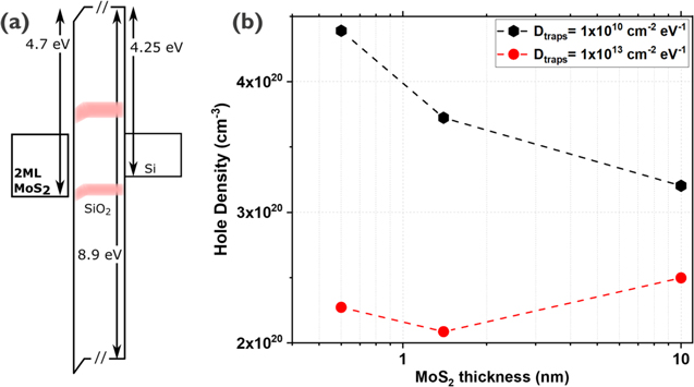
Figure 5. (a) Experimental band alignments obtained from IPE measurements done on 2ML MoS2 supported on SiO2 substrate [36]. We see that the valence band of MoS2 aligns slightly below the defect bands in SiO2. (b) Graph depicting the relationship between hole density, channel thickness and oxide trap density at −60 V on the backgate for a of 90 nm thick SiO2 substrate.
Download figure:
Standard image High-resolution imageOur hypothesis is further substantiated by performing semi classical simulations of MoS2 MOS structures with the presence of the lower band of defects in SiO2 (see Methods section). The purpose of the simulation was to estimate the expected improvement in hole density with different substrate defect band densities, assuming ideal contact interface for hole injection. A voltage of −60 V is applied across the MoS2–SiO2 interface. Maximum hole density is extracted for different thicknesses of the 2D semiconductor (0.6, 1.4, 10 nm) at different trap densities in the defect band (1 × 10¹³ and 1 × 1010 cm−2 eV−1). The results are plotted in figure 5(b). We observe that in the case of low trap density (1 × 1010 cm−2 eV−1), thin devices (0.6 nm) show the highest hole density. This is a result of the improved gate modulation on thinner channels with the low trap density having little effect on the accumulated charge. If the density of defect states in the oxide has a comparable magnitude as the density of injected carriers in the semiconductor, a significant part of the charge carriers (in this case holes since we consider the proximity of the VBM) will be trapped in the oxide and not be available for charge transport. Increasing the trap density to 1 × 1013 cm−2 eV−1, however, significantly reduces the hole density in the channel for all thicknesses and significantly changes the trend with thickness. The thickest channel now shows the highest hole density, exactly because the charge centroid is further away from the traps.
These observations imply that to achieve significant ambipolar transport in thin MoS2 channels, it is crucial to reduce the interface and oxide trap density, or to choose substrates with defect bands positioned far from the valence band edge of MoS2. To test this, we explore alternate substrates for MoS2 FETs.
3.3.1. SiO2 compared to hBN substrate
The aforementioned hypothesis is tested by comparing two dielectrics with significantly different trap densities: SiO2 and hBN. Although hBN has been demonstrated in the past to improve the performance of TMDC and graphene FETs [16, 37, 38], this is the first time a direct comparison of the same device on different substrates has been conducted. Furthermore, it is expected that the trap density of hBN is lower than that of SiO2, although there has been no study experimentally quantifying the defect density in hBN, till date. We fabricated a device with transferred contacts, first on a 90 nm SiO2 substrate, followed by electrical characterization and then transferred the whole device onto an hBN substrate, where it is electrically characterized again. The hBN flake supports the whole MoS2 flake (27 nm thick), which forms the semiconducting channel (figure 6(a)). Figure 6(b) depicts the measured transfer characteristics on SiO2 and hBN substrate. The first observation is that both on SiO2 and on hBN, this thick flake exhibits ambipolar transport. Furthermore, we measure a 10-fold increase in the p-ION for the same gate voltage, when shifting from the SiO2 substrate to the hBN substrate. This validates our hypothesis that reducing the substrates trap density improves ambipolar transport. This analysis is further supported by the schematic band alignment between MoS2 and hBN shown in figure 7(a). When taking into account the defect bands of hBN, assessed by optical analysis [32], it is clear these defect bands do not overlap with the valence band edge of MoS2, as in the case for SiO2 (see figure 5(a)). From this we conclude that we are able to better modulate the Fermi level and bring it to the valence band more effectively when MoS2 lies on hBN than on SiO2 substrate. It is interesting to note that in spite of the higher effective oxide thickness in the hBN case, the drain current is higher for both positive and negative gate voltages. This proves the positive impact a 2D substrate like hBN has on 2D material FETs.

Figure 6. (a) Schematic of the measurements. Initial measurement is done on SiO2 substrate after which the whole device is transferred onto a 21 nm hBN flake and measured again. (b) Transfer characteristics (measured at VDS = 1 V) of same device on SiO2 and hBN substrate respectively. We see that the p-branch of current increases upon the transfer from SiO2 substrate to the hBN substrate, while the n-branch only slightly increases.
Download figure:
Standard image High-resolution image
Figure 7. (a) Theoretical band alignment between MoS2, hBN and its defect bands. We see that the lower defect band is located inside the valence band of MoS2. (b) Transfer characteristics of multiple MoS2 devices on hBN, with different thicknesses. All devices have a nominal channel length of 7 μm and are measured at a VDS of 1 V.
Download figure:
Standard image High-resolution imageFurthermore, we fabricated MoS2 FETs with different thicknesses on hBN flake substrates using the transferred contacts approach. The processing and channel length of the different devices were kept identical to compare the p-branch in different devices. As postulated, when expanding the thickness-dependent analysis to devices on hBN, significant ambipolar transport is observed down to a MoS2 channel thickness of 2.6 nm (4ML), as shown in figure 7(b). Mono-layer MoS2/hBN device also show an onset of ambipolar transport, with a p-ION/IOFF of 15.
However, hBN is currently not a CMOS-compatible dielectric. Besides the difficulties of growing high quality large area synthetic hBN and its subsequent transfer from growth template wafer to device substrates, hBN possesses a relatively low dielectric constant, which contrasts with the high-κ dielectrics used in current CMOS technology. Therefore, demonstrating ambipolar transistors on hBN does not completely open a path for CMOS integration of MoS2 devices. Therefore, we investigate the use of Al2O3 as a substrate for MoS2 FETs.
3.3.2. Al2O3 as a suitable substrate
Our previous discussion confirmed that the oxide trap bands have to be carefully considered in order to observe ambipolar transport in MoS2 devices. Indeed, when comparing the experimental MoS2/Al2O3 band alignment [39] to the defect band of Al2O3 [33, 40], one can observe that the defect band is positioned far away from the valence band edge of MoS2, as shown in figure 8(b). According to our model, Al2O3 would therefore be a suitable and technologically relevant substrate for the demonstration of ambipolar transport in MoS2 FETs. To verify this claim, we fabricate a series of MoS2 devices of different thickness on 20 nm Al2O3 substrate, following the transferred contacts approach, as described in the methods section. The corresponding device transfer characteristics are presented in figure 8(a). It can be seen that all thicknesses show significant p-branch, which is consistent with our hypothesis. Interestingly, even a 2ML device (1.4 nm) shows clear ambipolar behavior, which considering previous reports, is the thinnest ambipolar MoS2 device demonstrated to date without any intrinsic/extrinsic doping, ionic gel gating or complex processing steps.

Figure 8. (a) Transfer characteristics of MoS2/Al2O3 devices with various MoS2 thicknesses. (b) Experimental band alignment between MoS2, Al2O3 and its defect bands. We see that the Al2O3 defect band overlaps above the conduction band minimum of 2ML MoS2. (c) ION/IOFF of the p-branch of devices of multiple thicknesses on SiO2, hBN and Al2O3. All devices have a nominal channel length of 7 μm and are measured at a VDS of 1 V. It can be observed that on hBN the thinner devices exhibit a relatively higher p-ION/IOFF, as compared to the case of SiO2 substrate. The ratio is further improved for Al2O3 substrate which shows nearly constant p-ION/IOFF down to 2 ML MoS2 devices.
Download figure:
Standard image High-resolution image
The summary of the ambipolar transport observed in all MoS2 FETs fabricated in this work is presented in figure 8(c). This graph depicts the ION/IOFF of the p-branch as a function of MoS2 thickness, for the three different substrates studied. p-ION was extracted as the current value at a back gate bias of −50 V. p-IOFF was extracted as the minimum current value measured. This value was extracted as the p-IOFF since the gate leakage current density was below this value in all devices. It can be seen that SiO2 only shows good p-ION/IOFF for devices with thickness in the range of 5–30 nm, which rapidly degrades for both thinner and thicker devices. hBN presents similar trends, however with higher p-ION/IOFF values in all cases. Al2O3, on the other hand, shows nearly constant p-ION/IOFF value for all thickness, from 1.4 nm (2ML) all the way to 52.7 nm. Furthermore, we have also measured the same devices at higher drain voltages with faster gate sweeps, which confirms the impact of the defect bands on the p-branch (see supplementary information section S2). These observations display the importance of carefully selecting the bottom dielectric in order to achieve ambipolar transport in MoS2 devices.
4. Conclusion
In summary, we demonstrate that FLP occurs not only at the metal-MoS2 interface, but also at MoS2-substrate interface. We observe that for an SiO2 substrate this pinning is caused by one of the SiO2 defect bands aligning with the valence band edge of bilayer MoS2, thereby deteriorating hole transport in thin MoS2 devices. We verify this hypothesis by fabricating MoS2 FETs of different channel thicknesses on substrates that have a more favorable defect band alignment, namely hBN and Al2O3. These devices are fabricated using a novel dry contact transfer process, enabling us to contact MoS2 flakes without E-beam lithography which has been demonstrated to reduce the p-branch of MoS2 FETs in this study. We find improved ambipolar transport for thinner channels, even down to a bilayer MoS2 FET, which to date is the thinnest ambipolar MoS2 device without any intrinsic/extrinsic doping or complex processing steps. We expect the p-branch to be further boosted by utilizing higher work function contacts in combination with defect band optimization of the underlying substrate. Although this study demonstrates ambipolar transport using back gated devices, the learning obtained from this study can be used to carefully select the top and back gate oxides in future research works. A top gate would result in the charge centroid moving away from the back gate oxide interface and the top gate oxide interface would be more critical. In general, our study highlights that MoS2 is indeed an ambipolar material, and the absence of ambipolar transport is strongly correlated to its dielectric environment and processing conditions.
Acknowledgments
The authors would like to thank C. J. L De La Rosa, U. Celano and M. Mascaro for the insightful discussions regarding ambipolar transport. We would also like to thank Y. Balaji for helping with the contact transfer technique and the Beyond CMOS program at IMEC for financial support.